- МЭМС и НЭМС датчики

Содержание
- 2. Дизайн МЭМС и НЭМС Design of MEMS&NEMS Принцип работы Набор элементов системы пассивные датчики актуаторы (приводы)
- 3. Датчики в различных устройствах МЭМС/НЭМС MEMS&NEMS sensor applications Транспорт Transportation Автомобильная безопасность, системы торможения и остановки
- 4. Термоэлектрический датчик Thermoelectric sensor Коэффициенты Зеебека по отношению к платине для некоторых металлов и поликремния. Seebeck
- 5. Датчик на основе pn-перехода P-N junction temperature sensor Вольт-амперная характеристика полупроводникового диода Direct bias Direct bias
- 6. Терморезистивный датчик Thermistor Большой терморезистивный коэффициент (0.2-0.3 %/K) Large temperature coefficient of resistance Малая теплоемкость Small
- 7. Физические свойства некоторых материалов НЭМС Physical properties of some NEMS materials
- 8. Инфракрасные датчики и массивы датчиков Infrared sensors and their arrays Illustration of a single sense element
- 9. Датчик газового потока Gas flow sensor Illustration of a micromachined mass flow sensor. Gas flow cools
- 10. Датчик СО - Carbon monoxide sensor Illustration of a carbon monoxide sensor, its equivalent circuit model,
- 11. Пьезорезистивный датчик Piezoresistors A typical thin metal foil strain gauge mounted on a backing film. Stretching
- 12. Пьезорезистивный датчик давления Piezoresistive pressure sensor The calibration and compensation functions are provided by specially designed
- 13. Последовательность производства датчика давления Technological stages of pressure sensor The first high-volume production of a pressure
- 14. Миниатюрный абсолютный пьезорезистивный датчик давления. Absolute pressure sensor. A miniature silicon-fusion-bonded absolute pressure sensor. (Courtesy of:
- 15. Photograph of the NovaSensor NPP-301, a premolded plastic, surface mount (SOIC-type) and absolute pressure sensor. (Courtesy
- 16. Photograph of a disposable blood pressure sensor for arterial-line measurement in intensive care units. The die
- 17. Высокотемпературный датчик давления High-temperature pressure sensor Photograph of an SOI-based pressure sensor rated for extended temperature
- 18. Пьезоэлектрический элемент (датчик или привод) Piezoelectric element (sensor or actuator) An illustration of the piezoelectric effect
- 19. Пьезоэлектрические коэффициенты различных материалов Piezoelectric coefficients (PbZrO3)
- 20. Датчики ускорения Acceleration sensor
- 21. Требования к датчикам ускорения Requirements to acceleration sensors Accelerometers for airbag crash sensing are rated for
- 22. Базовая структура датчика ускорения Base structure of acceleration sensor The basic structure of an accelerometer, consisting
- 23. Пьезорезистивный датчик ускорения Piezoresistive acceleration sensor Illustration of a piezoresistive accelerometer from Endevco Corp., fabricated using
- 24. Емкостной датчик Capacitor sensor Поперечная конфигурация Продольная конфигурация x0 Δx Δy ly
- 25. Емкостной датчик ускорения. Capacitive accelerometer. Illustration of a bulk micromachined capacitive accelerometer. The inertial mass in
- 26. Емкостной датчик ускорения – последовательность производства Production of capacitive accelerometer
- 27. Емкостной датчик ускорения. Capacitive accelerometer. Illustration of the basic structure of the ADXL family of surface
- 28. Емкостной датчик ускорения, произведенный с помощью DRIE. Capacitive accelerometer using DRIE. Scanning-electron micrograph of a DRIE
- 29. Сравнение пьезорезистивного, емкостного и электромагнитного методов измерения Comparison of different sensing
- 30. To be continued
- 32. Скачать презентацию
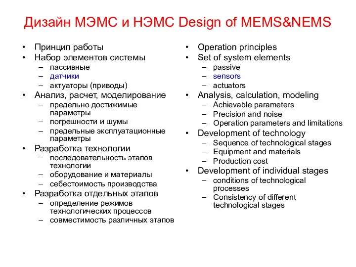
Дизайн МЭМС и НЭМС Design of MEMS&NEMS
Принцип работы
Набор элементов системы
пассивные
датчики
актуаторы
Дизайн МЭМС и НЭМС Design of MEMS&NEMS
Принцип работы
Набор элементов системы
пассивные
датчики
актуаторы
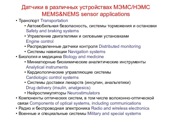
Датчики в различных устройствах МЭМС/НЭМС
MEMS&NEMS sensor applications
Транспорт Transportation
Автомобильная безопасность,
Датчики в различных устройствах МЭМС/НЭМС
MEMS&NEMS sensor applications
Транспорт Transportation
Автомобильная безопасность,
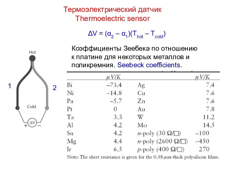
Термоэлектрический датчик
Thermoelectric sensor
Коэффициенты Зеебека по отношению к платине для некоторых металлов
Термоэлектрический датчик
Thermoelectric sensor
Коэффициенты Зеебека по отношению к платине для некоторых металлов
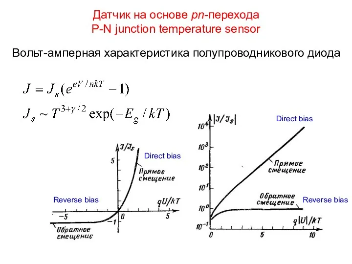
Датчик на основе pn-перехода
P-N junction temperature sensor
Вольт-амперная характеристика полупроводникового диода
Direct bias
Direct
Датчик на основе pn-перехода
P-N junction temperature sensor
Вольт-амперная характеристика полупроводникового диода
Direct bias
Direct
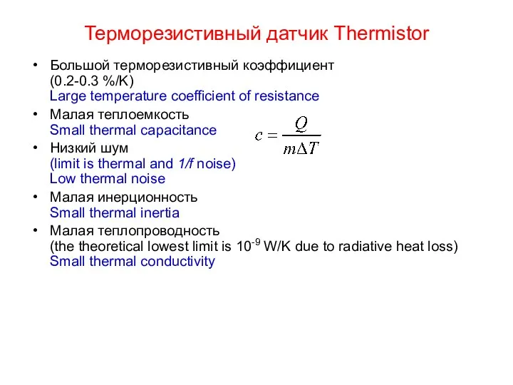
Терморезистивный датчик Thermistor
Большой терморезистивный коэффициент
(0.2-0.3 %/K)
Large temperature coefficient of resistance
Малая
Терморезистивный датчик Thermistor
Большой терморезистивный коэффициент
(0.2-0.3 %/K)
Large temperature coefficient of resistance
Малая
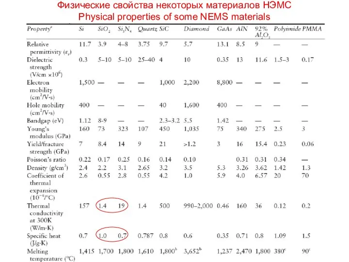
Физические свойства некоторых материалов НЭМС
Physical properties of some NEMS materials
Физические свойства некоторых материалов НЭМС
Physical properties of some NEMS materials
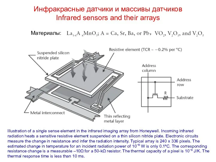
Инфракрасные датчики и массивы датчиков
Infrared sensors and their arrays
Illustration of a
Инфракрасные датчики и массивы датчиков
Infrared sensors and their arrays
Illustration of a
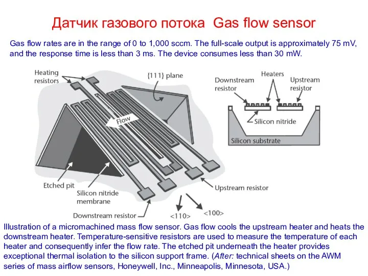
Датчик газового потока Gas flow sensor
Illustration of a micromachined mass flow
Датчик газового потока Gas flow sensor
Illustration of a micromachined mass flow
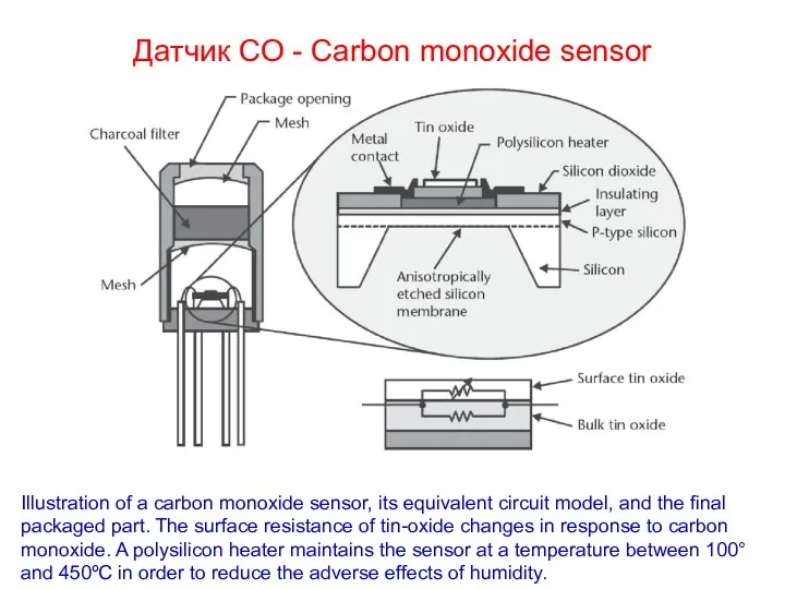
Датчик СО - Carbon monoxide sensor
Illustration of a carbon monoxide sensor,
Датчик СО - Carbon monoxide sensor
Illustration of a carbon monoxide sensor,
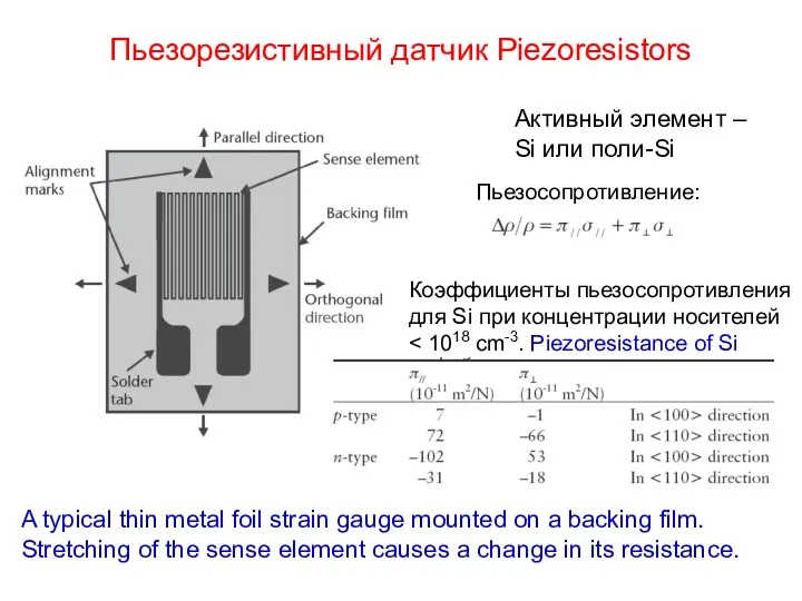
Пьезорезистивный датчик Piezoresistors
A typical thin metal foil strain gauge mounted on
Пьезорезистивный датчик Piezoresistors
A typical thin metal foil strain gauge mounted on
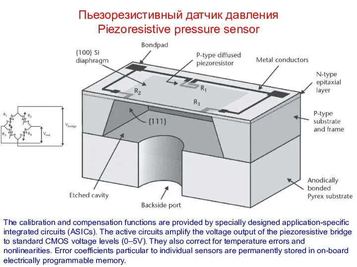
Пьезорезистивный датчик давления
Piezoresistive pressure sensor
The calibration and compensation functions are
Пьезорезистивный датчик давления
Piezoresistive pressure sensor
The calibration and compensation functions are
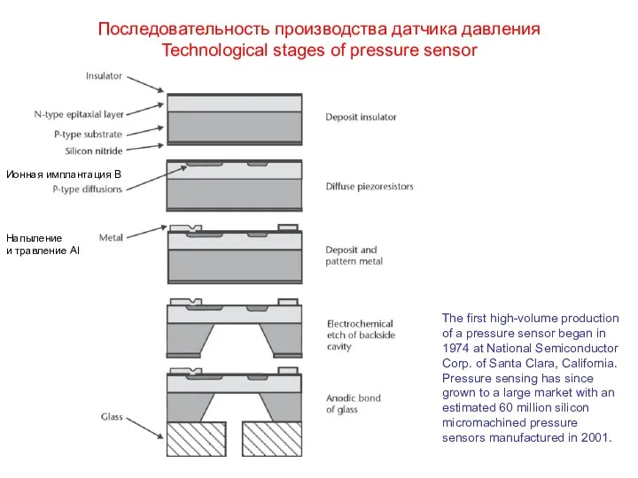
Последовательность производства датчика давления
Technological stages of pressure sensor
The first high-volume production
Последовательность производства датчика давления
Technological stages of pressure sensor
The first high-volume production
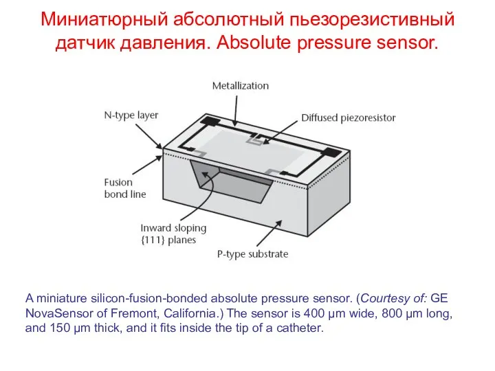
Миниатюрный абсолютный пьезорезистивный датчик давления. Absolute pressure sensor.
A miniature silicon-fusion-bonded absolute
Миниатюрный абсолютный пьезорезистивный датчик давления. Absolute pressure sensor.
A miniature silicon-fusion-bonded absolute
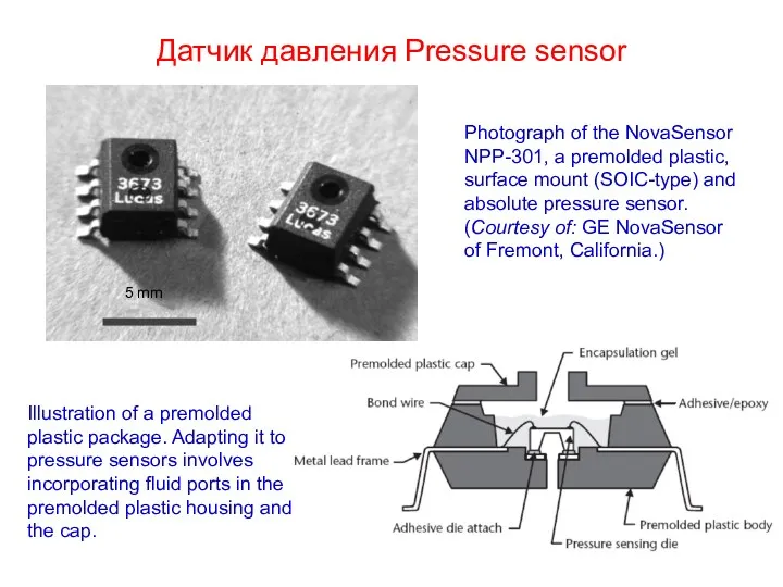
Photograph of the NovaSensor NPP-301, a premolded plastic, surface mount (SOIC-type)
Photograph of the NovaSensor NPP-301, a premolded plastic, surface mount (SOIC-type)
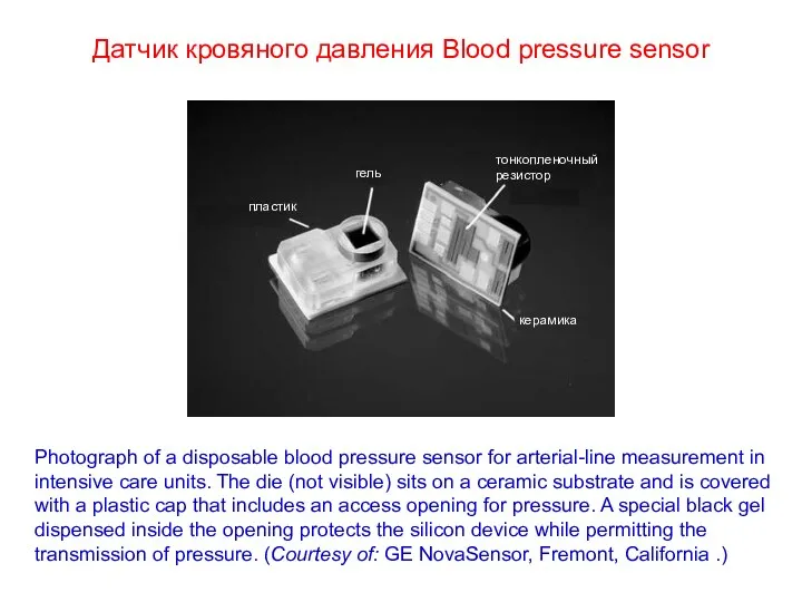
Photograph of a disposable blood pressure sensor for arterial-line measurement in
intensive
Photograph of a disposable blood pressure sensor for arterial-line measurement in
intensive
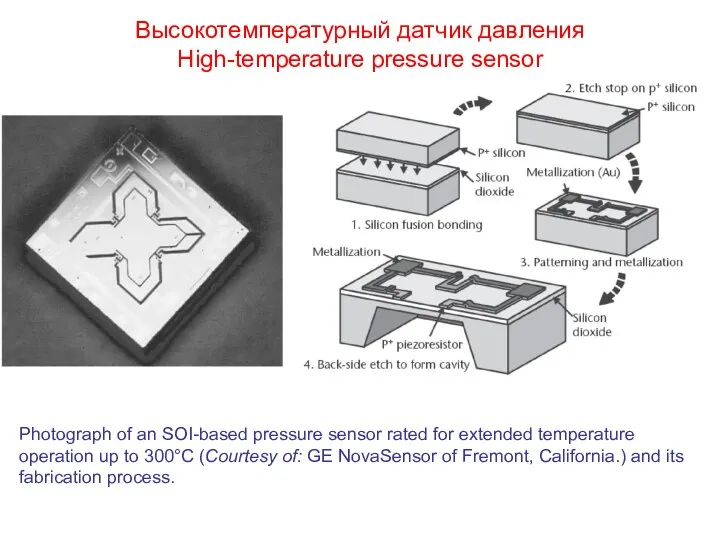
Высокотемпературный датчик давления
High-temperature pressure sensor
Photograph of an SOI-based pressure sensor
Высокотемпературный датчик давления
High-temperature pressure sensor
Photograph of an SOI-based pressure sensor
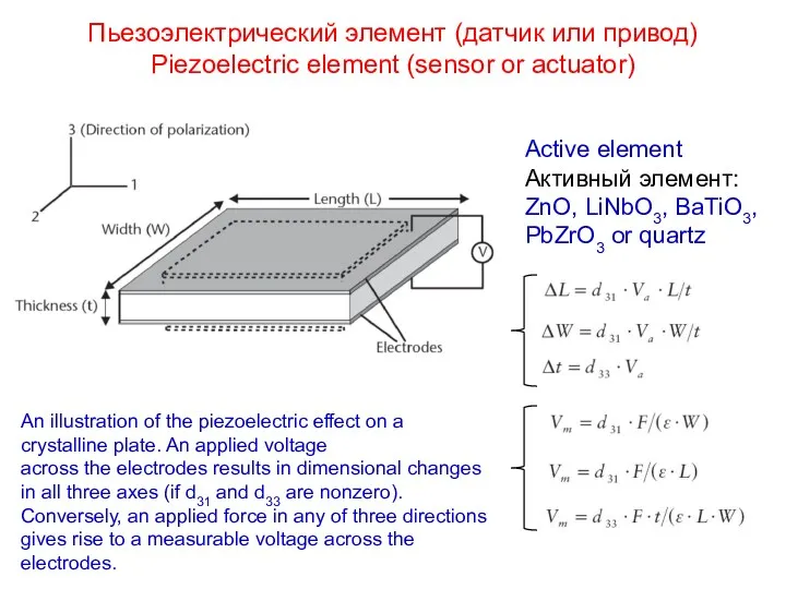
Пьезоэлектрический элемент (датчик или привод)
Piezoelectric element (sensor or actuator)
An illustration of
Пьезоэлектрический элемент (датчик или привод)
Piezoelectric element (sensor or actuator)
An illustration of
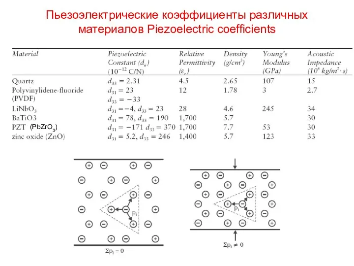
Пьезоэлектрические коэффициенты различных материалов Piezoelectric coefficients
(PbZrO3)
Пьезоэлектрические коэффициенты различных материалов Piezoelectric coefficients
(PbZrO3)
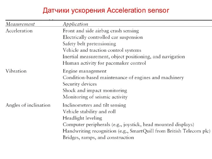
Датчики ускорения Acceleration sensor
Датчики ускорения Acceleration sensor
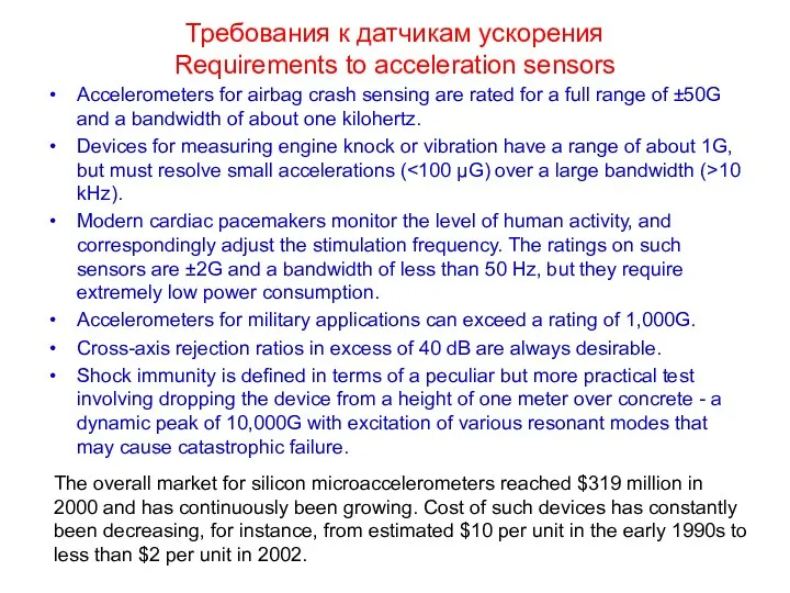
Требования к датчикам ускорения
Requirements to acceleration sensors
Accelerometers for airbag crash
Требования к датчикам ускорения
Requirements to acceleration sensors
Accelerometers for airbag crash
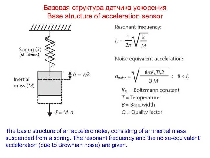
Базовая структура датчика ускорения
Base structure of acceleration sensor
The basic structure
Базовая структура датчика ускорения
Base structure of acceleration sensor
The basic structure
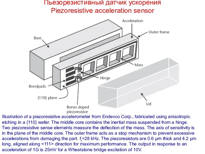
Пьезорезистивный датчик ускорения
Piezoresistive acceleration sensor
Illustration of a piezoresistive accelerometer from Endevco
Пьезорезистивный датчик ускорения
Piezoresistive acceleration sensor
Illustration of a piezoresistive accelerometer from Endevco
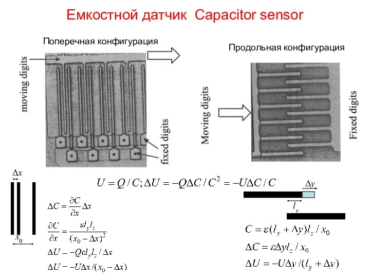
Емкостной датчик Capacitor sensor
Поперечная конфигурация
Продольная конфигурация
x0
Δx
Δy
ly
Емкостной датчик Capacitor sensor
Поперечная конфигурация
Продольная конфигурация
x0
Δx
Δy
ly
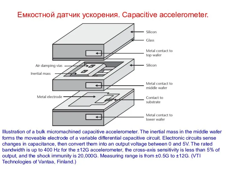
Емкостной датчик ускорения. Capacitive accelerometer.
Illustration of a bulk micromachined capacitive accelerometer.
Емкостной датчик ускорения. Capacitive accelerometer.
Illustration of a bulk micromachined capacitive accelerometer.
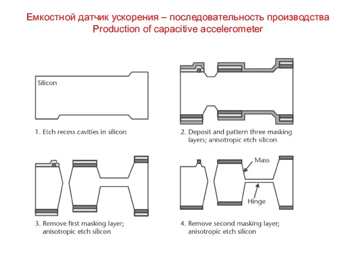
Емкостной датчик ускорения – последовательность производства
Production of capacitive accelerometer
Емкостной датчик ускорения – последовательность производства
Production of capacitive accelerometer
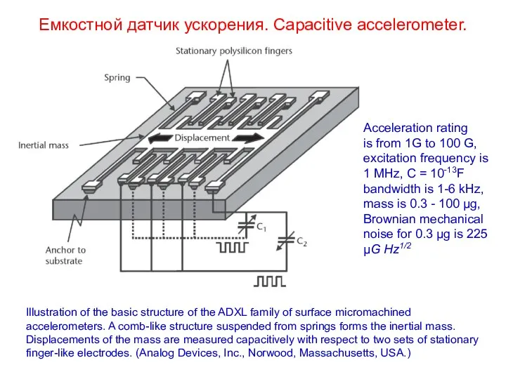
Емкостной датчик ускорения. Capacitive accelerometer.
Illustration of the basic structure of the
Емкостной датчик ускорения. Capacitive accelerometer.
Illustration of the basic structure of the
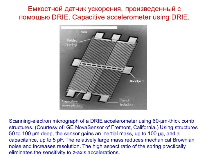
Емкостной датчик ускорения, произведенный с помощью DRIE. Capacitive accelerometer using DRIE.
Scanning-electron
Емкостной датчик ускорения, произведенный с помощью DRIE. Capacitive accelerometer using DRIE.
Scanning-electron
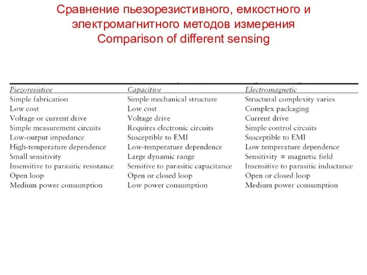
Сравнение пьезорезистивного, емкостного и электромагнитного методов измерения
Comparison of different sensing
Сравнение пьезорезистивного, емкостного и электромагнитного методов измерения
Comparison of different sensing

To be continued
To be continued
 Значение влажности в жизни человека
 26e1e5eed06e9616d6b0b1a82d75cb58
 Area, size and mass
 Постоянные магниты (8 класс)
 Инфракрасное, ультрафиолетовое и рентгеновское излучения. Их свойства и применение
 Физика и техника
 Проект Инженерный класс в московской школе. Практические ситуационные задачи и теоретические задачи
 Законы постоянного тока
 Основні уявлення та рівняння
 Баяндама Альберт Эйнштейн
 Векторный анализ и синтез сигналов. Программа “Вектор”
 Подготовка к ОГЭ по физике на уроке. Решение задач по физике различного типа и уровня сложности
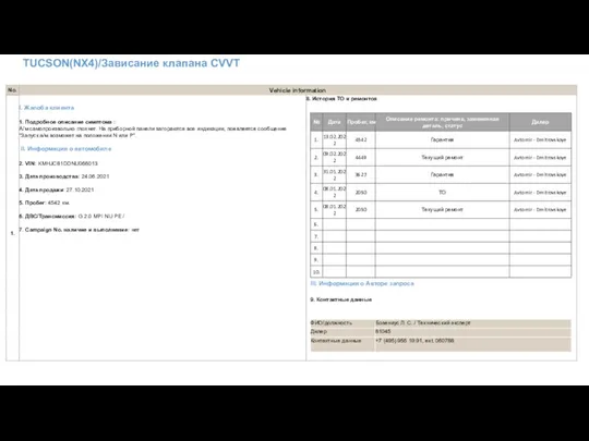 Tucson (NX 4). Зависание клапана CVVT
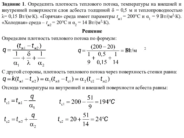 Теплопередача. Задачи
 Физика атома и атомных явлений
 Сила. Явление тяготения. Сила тяжести
 История развития нанотехнологий
 Алгоритмы решения физических задач
 Unusual modes pf transport
 Виды теплопередачи ( презентация к уроку)- 8 класс
 Получение и передача переменного электрического тока. Трансформатор
 Состав систем космического аппарата. Проведение литературного обзора
 Основы машиноведения
 Викторина по физике
 Summary of effective use 6
 Основы квантовой физики. Лазеры
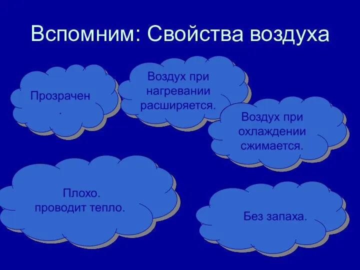 Свойства воздуха
 Система питания двигателя от впрыска топлива