- Gowin Semiconductor Corporation

Содержание
- 2. Agenda
- 3. Major R&D Centers Guangzhou Shanghai Hong Kong Jinan International Sales Guangzhou China (HQ) United Kingdom Hong
- 4. Locations: Guangdong, China (Corp HQ) San Jose, California (US HQ) Hong Kong (Asia HQ) Shandong, Shanghai,
- 5. Differentiating FPGA Features More Interfaces ADC, USB, SPMI, I3C On-Chip Memory Up to 16MB Hardened MCUs
- 6. GOWIN FPGA Product Families
- 7. GOWIN FPGA Embedded Processors
- 8. GOWIN FPGA On-Chip Memory Options 128Mbits DDR Data Width: 16-bits Clock Freq: 166MHz
- 9. Pin Compatible Devices GOWIN FPGAs may be pin-for-pin compatible with similar size devices from Lattice, Intel
- 10. Automotive Parts – Available Q1/Q2 2021 AEC-Q100 Level-2 Certification -40oC to +105oC LittleBee GW1N-4 QN88 Qualification
- 11. Flash-Based, Non-Volatile, Instant On, Low Power, Low Cost, Small Package Options . LittleBee GW1N (Base Family)
- 12. LittleBee GW1NR with On-Chip Memory On-Chip Memory up to 128Mbits* (16KBytes) *package dependent . On-Chip Memory
- 13. LittleBee µSoC GW1NS Family ARM Cortex-M3*, USB-PHY*, ADC*, On-Chip Memory* *package dependent . Hardcore ARM Cortex-M3
- 14. LittleBee µSoC GW1NSE SecureFPGA SecureFPGA Root-of-Trust using Physically Unclonable Functionality (PUF) Technology ..
- 15. LittleBee GW1NZ Ultra-Low Power Ultra-Low Power, Lowest Cost, Flash-Based, Non-Volatile, Instant On .. Core Voltage LV
- 16. LittleBee GW1NRF Bluetooth Low Energy (BLE) BLE 5.0, 4K LUTs FPGA, Optimized 32-bit Processor . ..
- 17. Arora GW2A family 55nm SRAM Technology, High Performance DSP, High-Speed LVDS, Abundant B-SRAM .. GW2A Part
- 18. Arora GW2AR Family with On-Chip Memory 16MB DDR SDRAM or 8MB DDR pSRAM or 8MB SDR
- 19. Arora GW2AN-18 with On-Chip Flash – Available Q1 2021 Adds I2C Configuration, 2MB Non-Volatile NOR FLASH,
- 20. GW5AT 128K LUTs – Targeting 2021 Release Third Generation, 22nm SRAM Technology, High-Speed Transceivers .. GW5AT
- 21. GOWIN Product Roadmap 2014 2015 2016 2017 2018 2019 2020 2021 2022 2023 500K 100K 50K
- 22. Register as a Member to Access Documents and Download Data Member Login Provides Unrestricted Access to
- 23. GOWIN EDA Tool: FPGA Designer, Firmware Development DOWNLOAD GOWIN EDA – Latest Version Gowin®EDA_Gowin V1.9.5.01_win Licensed
- 24. GOWIN EDA® FPGA Designer Operating System Windows or Linux (inc. Ubuntu) Freely Licensed Fixed or Floating
- 25. RISC-V Core DDR/DDR2/DDR3* Controller PCI Controller pSRAM Controller SDRAM Controller I3C Master & Slave MIPI-TX-D-PHY MIPI-RX-D-PHY
- 26. GOWIN GoAI 2.0 Machine Learning (ML) Targets Low Cost, Low Power, Edge AI Applications Deploy Machine
- 27. GOWIN GoAI 2.0 Machine Learning Solution ‘1-Click’ Development Goal (Windows or Linux) Classification Algorithms Person Detection,
- 28. GOWIN GoAI 2.0 Evaluation Boards DK-GOAI-GW1NSR4C DK-GOAI-GW2A55PBGA484 Include the following Sensors Camera OV2640 1600x1200 2x Microphone
- 29. LittleBee GW1NRF Bluetooth Development Kit GW1NRF Eval Board GW1NRF Single Package Bluetooth 5.0 Low Energy IC
- 30. LittleBee GW1N Development Boards DK-START-GW1N1 DK-START-GW1NZ DK-START-GW1N4 DK-START-GW1N9 GW1NZ Eval Board GW1NZ-LV1FN32 GW1NZ-ZV1FN32 LVDS GPIO GW1N-1
- 31. LittleBee GW1NS µSoC Development Boards DK-START-GW1NSR2 DK-START-GW1NS2 DK-START-GW1NS4-QN48 DK-START-GW1NSR4-QN48 GW1NS-2 Eval Board GW1NS-UX2CLQ144 ARM Cortex-M3 LVDS
- 32. Arora GW2A Development Boards DK-START-GW2AR18 DK-START-GW2A18 DK-VIDEO-GW2A18-PG484 DK-START-GW2A55-PG484 GW2A-18 Eval Board GW2A-LV18PG256 2GB DDR3 External Memory
- 34. Скачать презентацию
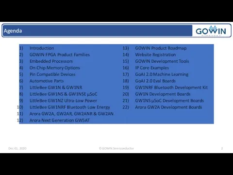
Agenda
Agenda
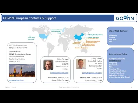
Major R&D Centers
Guangzhou
Shanghai
Hong Kong
Jinan
International Sales
Guangzhou China (HQ)
United Kingdom
Hong Kong
San Jose USA
Korea
Shandong
Major R&D Centers
Guangzhou
Shanghai
Hong Kong
Jinan
International Sales
Guangzhou China (HQ)
United Kingdom
Hong Kong
San Jose USA
Korea
Shandong
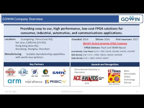
Locations: Guangdong, China (Corp HQ)
San Jose, California (US HQ)
Hong Kong (Asia HQ)
Shandong,
Locations: Guangdong, China (Corp HQ)
San Jose, California (US HQ)
Hong Kong (Asia HQ)
Shandong,
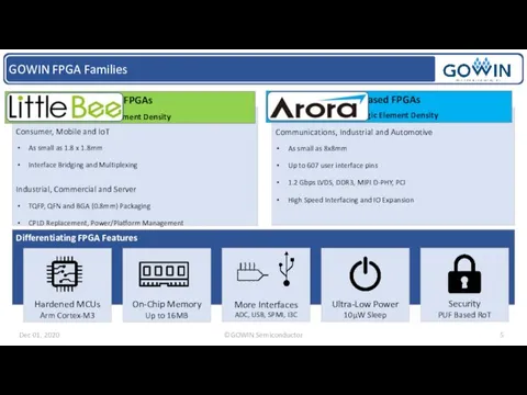
Differentiating FPGA Features
More Interfaces
ADC, USB, SPMI, I3C
On-Chip Memory
Up to 16MB
Hardened MCUs
Arm
Differentiating FPGA Features
More Interfaces
ADC, USB, SPMI, I3C
On-Chip Memory
Up to 16MB
Hardened MCUs
Arm
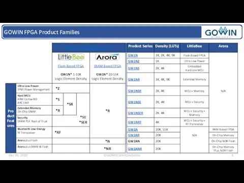
GOWIN FPGA Product Families
GOWIN FPGA Product Families
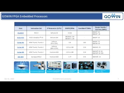
GOWIN FPGA Embedded Processors
GOWIN FPGA Embedded Processors
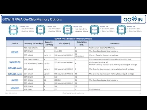
GOWIN FPGA On-Chip Memory Options
128Mbits DDR
Data Width: 16-bits
Clock Freq: 166MHz
GOWIN FPGA On-Chip Memory Options
128Mbits DDR
Data Width: 16-bits
Clock Freq: 166MHz
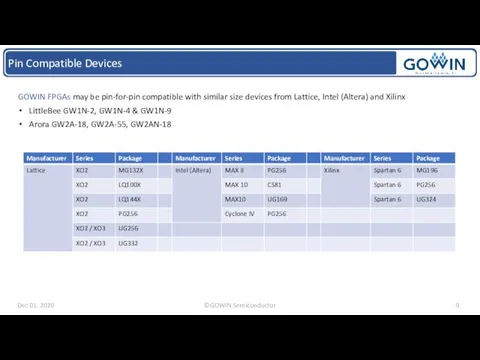
Pin Compatible Devices
GOWIN FPGAs may be pin-for-pin compatible with similar size
Pin Compatible Devices
GOWIN FPGAs may be pin-for-pin compatible with similar size
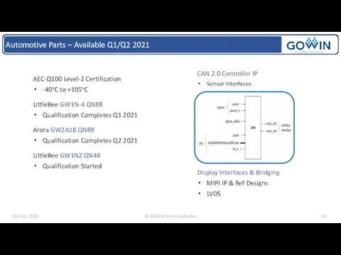
Automotive Parts – Available Q1/Q2 2021
AEC-Q100 Level-2 Certification
-40oC to +105oC
LittleBee GW1N-4
Automotive Parts – Available Q1/Q2 2021
AEC-Q100 Level-2 Certification
-40oC to +105oC
LittleBee GW1N-4
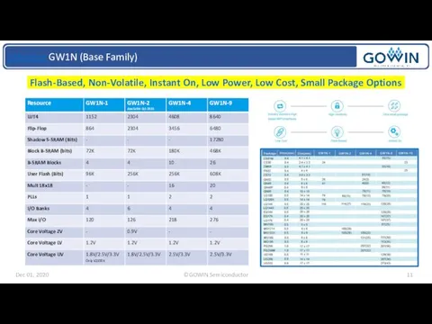
Flash-Based, Non-Volatile, Instant On, Low Power, Low Cost, Small Package
Flash-Based, Non-Volatile, Instant On, Low Power, Low Cost, Small Package
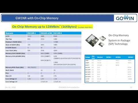
LittleBee GW1NR with On-Chip Memory
On-Chip Memory up to 128Mbits* (16KBytes)
LittleBee GW1NR with On-Chip Memory
On-Chip Memory up to 128Mbits* (16KBytes)
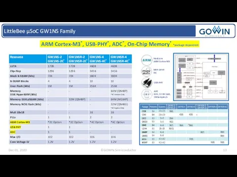
LittleBee µSoC GW1NS Family
ARM Cortex-M3*, USB-PHY*, ADC*, On-Chip Memory* *package
LittleBee µSoC GW1NS Family
ARM Cortex-M3*, USB-PHY*, ADC*, On-Chip Memory* *package
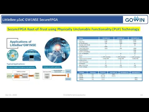
LittleBee µSoC GW1NSE SecureFPGA
SecureFPGA Root-of-Trust using Physically Unclonable Functionality (PUF)
LittleBee µSoC GW1NSE SecureFPGA
SecureFPGA Root-of-Trust using Physically Unclonable Functionality (PUF)
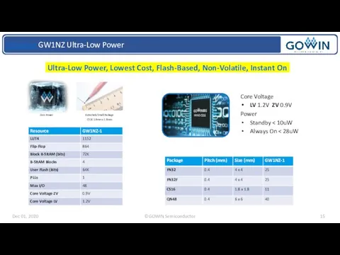
LittleBee GW1NZ Ultra-Low Power
Ultra-Low Power, Lowest Cost, Flash-Based, Non-Volatile, Instant
LittleBee GW1NZ Ultra-Low Power
Ultra-Low Power, Lowest Cost, Flash-Based, Non-Volatile, Instant
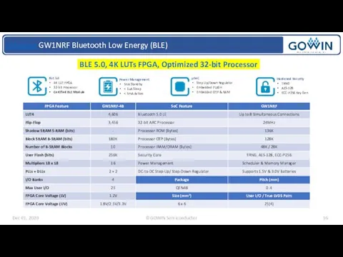
LittleBee GW1NRF Bluetooth Low Energy (BLE)
BLE 5.0, 4K LUTs FPGA,
LittleBee GW1NRF Bluetooth Low Energy (BLE)
BLE 5.0, 4K LUTs FPGA,
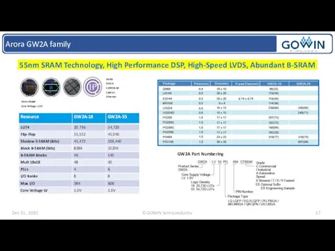
Arora GW2A family
55nm SRAM Technology, High Performance DSP, High-Speed LVDS,
Arora GW2A family
55nm SRAM Technology, High Performance DSP, High-Speed LVDS,
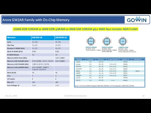
Arora GW2AR Family with On-Chip Memory
16MB DDR SDRAM or 8MB
Arora GW2AR Family with On-Chip Memory
16MB DDR SDRAM or 8MB
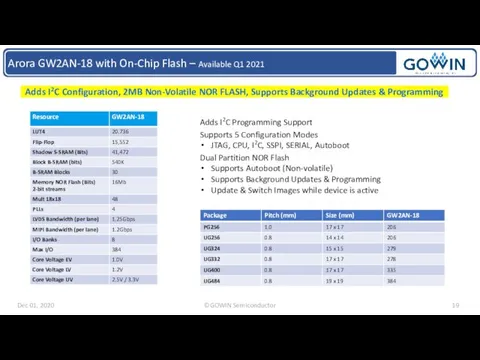
Arora GW2AN-18 with On-Chip Flash – Available Q1 2021
Adds I2C
Arora GW2AN-18 with On-Chip Flash – Available Q1 2021
Adds I2C
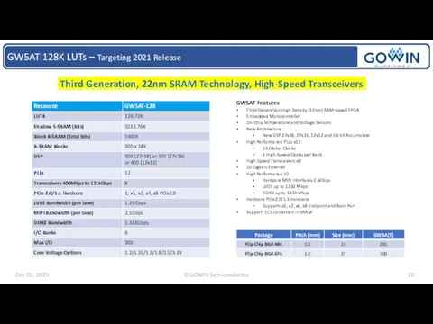
GW5AT 128K LUTs – Targeting 2021 Release
Third Generation, 22nm SRAM
GW5AT 128K LUTs – Targeting 2021 Release
Third Generation, 22nm SRAM
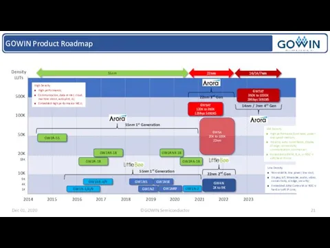
GOWIN Product Roadmap
2014 2015 2016 2017 2018 2019 2020 2021 2022
GOWIN Product Roadmap
2014 2015 2016 2017 2018 2019 2020 2021 2022
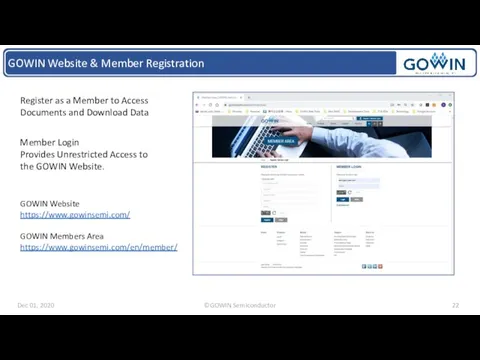
Register as a Member to Access Documents and Download Data
Member Login
Provides
Register as a Member to Access Documents and Download Data
Member Login
Provides
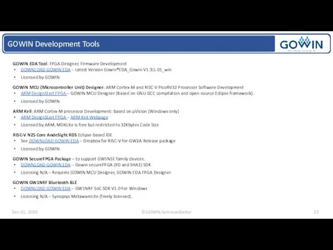
GOWIN EDA Tool: FPGA Designer, Firmware Development
DOWNLOAD GOWIN EDA – Latest
GOWIN EDA Tool: FPGA Designer, Firmware Development
DOWNLOAD GOWIN EDA – Latest
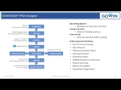
GOWIN EDA® FPGA Designer
Operating System
Windows or Linux (inc. Ubuntu)
Freely Licensed
Fixed or
GOWIN EDA® FPGA Designer
Operating System
Windows or Linux (inc. Ubuntu)
Freely Licensed
Fixed or
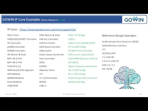
RISC-V Core
DDR/DDR2/DDR3* Controller
PCI Controller
pSRAM Controller
SDRAM Controller
I3C Master & Slave
MIPI-TX-D-PHY
MIPI-RX-D-PHY
FIFO/FIFO_SC
RAM-Based-Shift-Registers
DSP Modules
BSRAM Modules
Clock
RISC-V Core
DDR/DDR2/DDR3* Controller
PCI Controller
pSRAM Controller
SDRAM Controller
I3C Master & Slave
MIPI-TX-D-PHY
MIPI-RX-D-PHY
FIFO/FIFO_SC
RAM-Based-Shift-Registers
DSP Modules
BSRAM Modules
Clock
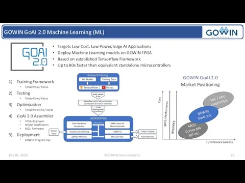
GOWIN GoAI 2.0 Machine Learning (ML)
Targets Low Cost, Low Power, Edge
GOWIN GoAI 2.0 Machine Learning (ML)
Targets Low Cost, Low Power, Edge
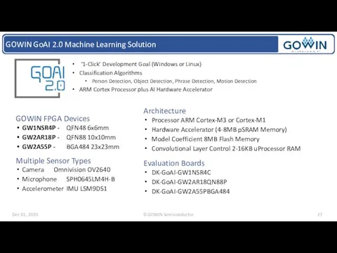
GOWIN GoAI 2.0 Machine Learning Solution
‘1-Click’ Development Goal (Windows or Linux)
Classification
GOWIN GoAI 2.0 Machine Learning Solution
‘1-Click’ Development Goal (Windows or Linux)
Classification
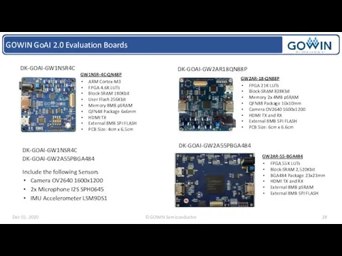
GOWIN GoAI 2.0 Evaluation Boards
DK-GOAI-GW1NSR4C
DK-GOAI-GW2A55PBGA484
Include the following Sensors
Camera OV2640 1600x1200
2x Microphone
GOWIN GoAI 2.0 Evaluation Boards
DK-GOAI-GW1NSR4C
DK-GOAI-GW2A55PBGA484
Include the following Sensors
Camera OV2640 1600x1200
2x Microphone
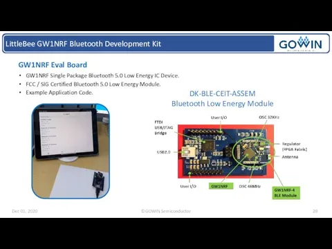
LittleBee GW1NRF Bluetooth Development Kit
GW1NRF Eval Board
GW1NRF Single Package Bluetooth
LittleBee GW1NRF Bluetooth Development Kit
GW1NRF Eval Board
GW1NRF Single Package Bluetooth
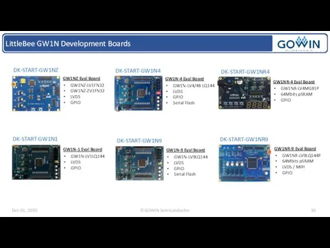
LittleBee GW1N Development Boards
DK-START-GW1N1
DK-START-GW1NZ
DK-START-GW1N4
DK-START-GW1N9
GW1NZ Eval Board
GW1NZ-LV1FN32
GW1NZ-ZV1FN32
LVDS
GPIO
GW1N-1 Eval Board
GW1N-LV1LQ144
LVDS
GPIO
GW1N-9
LittleBee GW1N Development Boards
DK-START-GW1N1
DK-START-GW1NZ
DK-START-GW1N4
DK-START-GW1N9
GW1NZ Eval Board
GW1NZ-LV1FN32
GW1NZ-ZV1FN32
LVDS
GPIO
GW1N-1 Eval Board
GW1N-LV1LQ144
LVDS
GPIO
GW1N-9
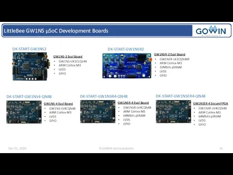
LittleBee GW1NS µSoC Development Boards
DK-START-GW1NSR2
DK-START-GW1NS2
DK-START-GW1NS4-QN48
DK-START-GW1NSR4-QN48
GW1NS-2 Eval Board
GW1NS-UX2CLQ144
ARM Cortex-M3
LVDS
GPIO
GW1NSR-2 Eval Board
LittleBee GW1NS µSoC Development Boards
DK-START-GW1NSR2
DK-START-GW1NS2
DK-START-GW1NS4-QN48
DK-START-GW1NSR4-QN48
GW1NS-2 Eval Board
GW1NS-UX2CLQ144
ARM Cortex-M3
LVDS
GPIO
GW1NSR-2 Eval Board
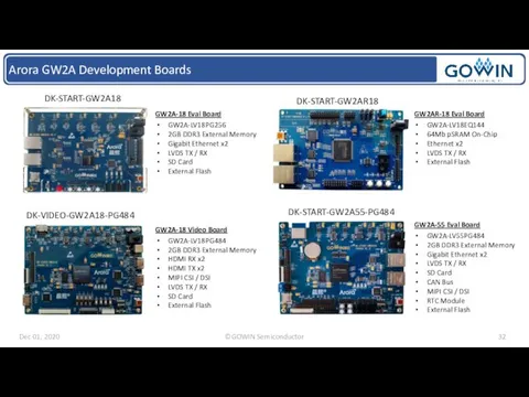
Arora GW2A Development Boards
DK-START-GW2AR18
DK-START-GW2A18
DK-VIDEO-GW2A18-PG484
DK-START-GW2A55-PG484
GW2A-18 Eval Board
GW2A-LV18PG256
2GB DDR3 External Memory
Gigabit Ethernet
Arora GW2A Development Boards
DK-START-GW2AR18
DK-START-GW2A18
DK-VIDEO-GW2A18-PG484
DK-START-GW2A55-PG484
GW2A-18 Eval Board
GW2A-LV18PG256
2GB DDR3 External Memory
Gigabit Ethernet
 Сварочная робототехника
 Анализ причин аварий строительных конструкций. Реконструкция. Лекция 1
 Антон Павлович Чехов
 Страна городов
 Пальчиковая гимнастика в рисунках и стихах.
 Градусная сетка
 Тест по истории искусства XIX века
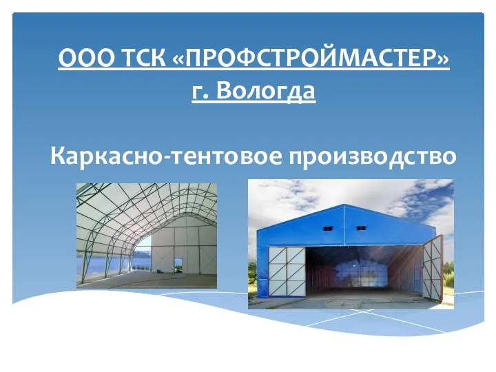 Каркасно-тентовое производство
 Новинки электронных технологий представленные осенью 2019 года
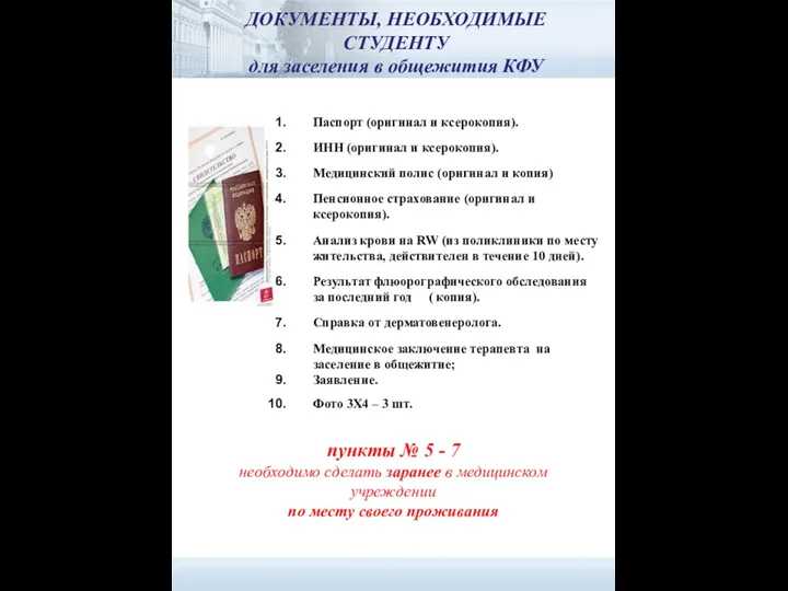 Документы для заселения в общежития КФУ
 Готовность к школе
 викторина по теме Культура бурятского народа для 5-6 классов.
 Причастие как часть речи
 Государственное регулирование. Основы коммерческой деятельности
 Библиотечно-библиографическая классификация
 Презентация для изучения словарных слов (овощи). 3 класс
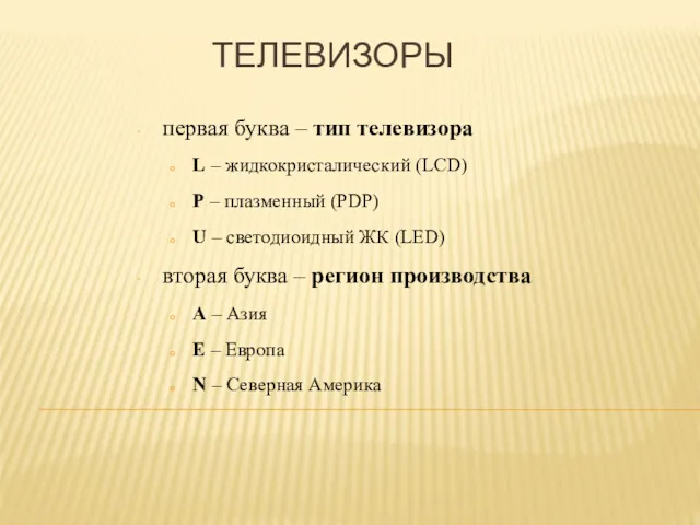 Samsung - Расшифровка моделей
 Богословие IV века. Святой Кирилл Иерусалимский (315-387 годы)
 Волейбол. Встречная передача и прием мяча сверху и снизу. Верхняя прямая подача, прием с подачи
 Фридрих Вильгельм Йозеф фон Шеллинг
 Традиции и обычаи Индии.
 Тесты
Тесты Классификация научных исследований. Наука и научный метод
 Раймон Клод Фердинанд Арон
 Тіс тіндерінің тісжегіден басқа аурулары
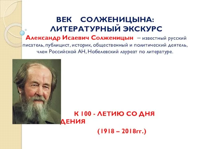 Произведения А.И. Солженицына
 урок безопасности
 Образ помещика. Плюшкин. Мертвые души