- Transistors

Содержание
- 2. Introduction This lecture introduces the transistor. Transistors are solid-state devices similar in some ways to the
- 3. Amplification Amplification is one of the most basic ideas in electronics. Amplifiers make sounds louder and
- 4. Amplification (1) Fig. 5-1 Amplifiers provide gain. Gain can be measured in several ways. If an
- 5. Calculation of the power gain
- 6. Power gain Only amplifiers provide a power gain. Other devices might give a voltage gain or
- 7. Amplification (2) Even though power gain seems to be the important idea, some amplifiers are classified
- 8. Amplification (3) Fig. 5-2 Small-signal and large-signal amplifiers.
- 9. Amplification (4) In electronics, gain is not expressed in volts, amperes, or watts. If voltage gain
- 10. Transistors Transistors provide the power gain that is needed for most electronic applications. They also can
- 11. Transistors (1) Fig. 5-3 NPN transistor structure.
- 12. Transistors (2) The transistor regions shown in Fig. 5-3 are named emitter, collector, and base. The
- 13. Transistors (3) The transistor shown in Fig. 5-3 would be classified as an NPN transistor. Another
- 14. Transistors (4) Fig. 5-4 Transistor structures and symbols. The two transistor junctions must be biased properly.
- 15. Transistors (5) Fig. 5-5 Biasing the transistor junctions. The base-emitter junction must be forward-biased to turn
- 16. Transistors (6) The large difference in junction resistance makes the transistor capable of power gain. Assume
- 17. Transistors (7) Fig. 5-6 Comparing junction resistances.
- 18. Transistors (8) If the current through RCB happened to be equal to the current through RBE,
- 19. Transistors (9) Figure 5-7 shows why the collector-base junction current is high. The collector-base voltage VCB
- 20. Transistors (10) Fig. 5-7 NPN transistor currents.
- 21. Transistors (11) With so few electron-hole combinations in the base region, the base current is very
- 22. Transistors (12) The current equation for Fig. 5-7 is IE = IC + IB By using
- 23. Transistors (13) Current will continue to flow from the emitter to the collector, but it does
- 24. Calculation of transistor’s current
- 25. Transistors (14) The characteristic is called β (Greek beta), or hFE: What is the β of
- 26. Calculation of β
- 27. Transistors (15) Figure 5-8 shows the flow from emitter to collector as hole current. In an
- 28. Transistors (16) Fig. 5-8 PNP transistor currents.
- 29. Characteristic Curves As with diodes, transistor characteristic curves can provide much information. There are many types
- 30. Fig. 5-9 A collector family of curves for an NPN transistor.
- 31. Characteristic Curves (1) Figure 5-10 shows a circuit that can be used to measure the data
- 32. Fig. 5-10 Circuit for collecting transistor data.
- 33. Characteristic Curves (2) The variable resistor in Fig. 5-10 is adjusted to produce the desired level
- 34. Characteristic Curves (3) The two prior calculations reveal another act about transistors. Not only does β
- 35. Fig. 5-11 Calculating βac with characteristic curves There is no significant difference between βdc and βac
- 36. Transistors at high frequencies At high frequencies the ac current gain of BJTs starts to fall
- 37. Characteristic Curves (4) It is standard practice to plot positive values to the right on the
- 38. Fig. 5-12 A collector family of curves for a PNP transistor.
- 39. Characteristic Curves (5) The transfer characteristic curves shown in Fig. 5-13 are another example of how
- 40. Fig. 5-13 Comparing silicon and germanium transistors.
- 41. Transistor Data Transistor manufacturers prepare data sheets that detail the mechanical, thermal, and electrical characteristics of
- 42. Transistor Data (1) Comparing two transistors often shows that they are very similar. For example, the
- 44. Transistor case styles There are hundreds of transistor case styles. Most are registered with the Joint
- 45. Transistor replacement In some cases the part number cannot be found in any of the available
- 46. Transistor Testing One way to test transistors is to use a curve tracer. This technique is
- 47. Transistor Testing Fig. 5-19(a) Atlas DCA Pro curve tracer
- 48. Transistor Testing Fig. 5-19(b) Atlas DCA Pro curve analyzer
- 49. Transistor Testing (1) A few transistor types may show a gradual loss of power gain. Radio-frequency
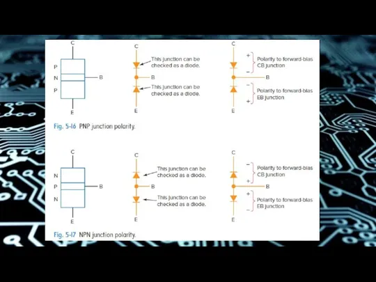
- 50. Transistor Testing (2) A good transistor has two PN junctions. Both can be checked with an
- 52. Transistor Testing (3) The resistor will be used to provide the transistor with a small amount
- 53. Transistor Testing (4) Fig. 5-18 Checking NPN gain.
- 54. Transistor Testing (4) Transistors have some leakage current. This is due to minority carrier action. One
- 55. Transistor Testing (5) With the base terminal open, any current leaking across the reverse-biased collector-base junction
- 56. Other Transistor Types Bipolar transistors use both holes and electrons as current carriers. A unipolar (one-polarity)
- 57. Other Transistor Types Fig. 5-20 An N-channel JFET.
- 58. Other Transistor Types (1) The JFET operates in the depletion mode. A control voltage at the
- 59. Other Transistor Types (2) Examine the curves of Fig. 5-21. Notice that as the voltage from
- 60. Other Transistor Types (3) Fig. 5-21 Characteristic curves of a JFET.
- 61. Other Transistor Types (4) These are important differences: (1) The bipolar device is current-controlled. (2) The
- 62. Other Transistor Types (5) Field-effect transistors (FETs) do not require any gate current for operation. This
- 63. Other Transistor Types (5) Fig. 5-22 An N-channel MOSFET.
- 64. Other Transistor Types (6) Early MOSFETs were very delicate. The thin oxide insulator was easily damaged
- 65. Other Transistor Types (7) The gate voltage in a MOSFET circuit can be of either polarity
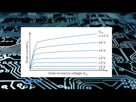
- 66. Other Transistor Types (8) Figure 5-23 shows a family of curves for an N-channel enhancement-mode device.
- 67. Other Transistor Types (9) Fig. 5-23 Enhancement-mode characteristic curves.
- 68. Other Transistor Types (10) Figure 5-24 shows a transistor family tree. Note that the enhancement-mode symbols
- 69. Fig. 5-24 A transistor family tree.
- 70. Phototransistors What if a transistor could be controlled by something else? How about light? One can
- 71. Phototransistors (1) Fig. 5-25 Phototransistors. Fig. 5-26 Phototransistor-controlled lighting.
- 72. Phototransistors (2) The collector is several volts positive with respect to the emitter. With no light
- 73. Phototransistors (3) Phototransistors can also be used in optoisolators (also called optocouplers). Figure 5-27 shows the
- 74. Phototransistors (3) Photo MOSFET transistors are another possibility. Figure 5-28 shows a gallium arsenide, infrared-emitting diode
- 75. Power Transistors Transistors can be divided into two broad categories: small-signal devices and power devices. When
- 76. Power Transistors (1) A 2N2222A conducting 200 mA and dropping 9 V (that’s 1.8 W) can
- 77. Power Transistors (2) Figure 5-29 shows that there is a significant difference in transistor case sizes.
- 78. Power Transistors (3) Fig. 5-29 A small-signal transistor and a power transistor. Fig. 5-30 Power derating
- 79. Power Transistors (4) Heat is one of biggest factors in the failure of electronic devices, and
- 80. Fig. 5-31 Safe limits of FET operation.
- 81. Power Transistors (5) The most obvious limits are the maximum safe current and the maximum safe
- 82. Fig. 5-32 Safe limits of BJT operation.
- 83. Power Transistors (6) Notice the curve between points 2 and 3. It has a steeper slope
- 84. Fig. 5-33 Constant power curve.
- 85. Power Transistors (7) If the collector characteristic curves are extended to include higher voltages, collector breakdown
- 86. Fig. 5-34 Collector breakdown.
- 87. Power Transistors (8) Figure 5-35 shows the safe operating area (SOA) curves for a power MOSFET.
- 88. Power Transistors (9) Figure 5-36 shows the SOA curves for a 2N6284 Darlington power transistor. Pay
- 89. Power Transistors (10) Figure 5-37 shows the internal circuit for a 2N6284 Darlington power transistor. The
- 90. Fig. 5-37 2N6284 Darlington Power internal circuit and TO-3 case.
- 91. Power Transistors (11) In addition to extra components being placed inside transistor cases, there can be
- 92. Fig. 5-38 Power VMOS structure.
- 93. Power Transistors (12) Figure 5-39 shows the schematic symbol for the transistor shown in Fig. 5-38.
- 94. Fig. 5-39 Enhancement mode power N-channel MOSFET schematic symbol shows the integral body diode.
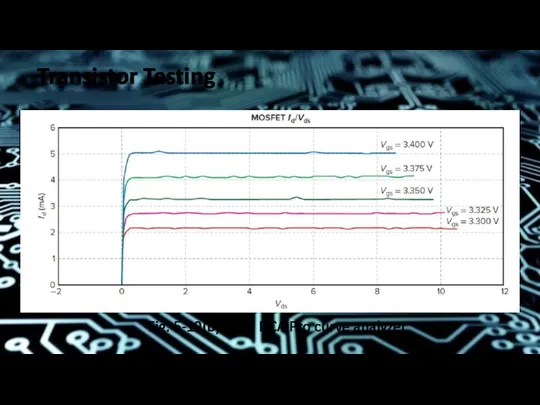
- 95. Power Transistors (13) Figure 5-40 shows the VDS versus ID characteristic curves for an enhancement mode
- 96. Fig. 5-40 Power enhancement-type MOSFET characteristic curves
- 97. Power Transistors (14) With high-power transistors, the drive requirements become important. Both BJT and MOSFET transistors
- 98. Power Transistors (15) Yet another advantage of MOSFETs is that they don’t have a problem with
- 99. Power Transistors (16) The insulated gate bipolar transistor (IGBT) is yet another choice. Figure 5-41 shows
- 100. Power Transistors (17) Semiconductor manufac-turers such as ON SemiconductorTM sell unpack-aged dies such as the NGTD21T65F2,
- 101. Power Transistors (18) Figure 5-42 shows the saturation curves and the case (package) for one IGBT.
- 102. Fig. 5-42 IGBT collector current versus saturation voltage curves and case style.
- 103. Power Transistors (19) IGBTs can be compared to MOSFETs, as shown in Table 5-2.
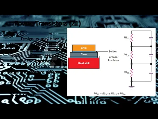
- 104. Power Transistors (20) The thermal model of a transistor is shown in Fig. 5-43. Heat flow
- 105. Power Transistors (21) Designers may have to choose a large metal heat sink or use fan
- 106. Power Transistors (22) The thermal model shown in Fig. 5-43 also shows capacitors; these model thermal
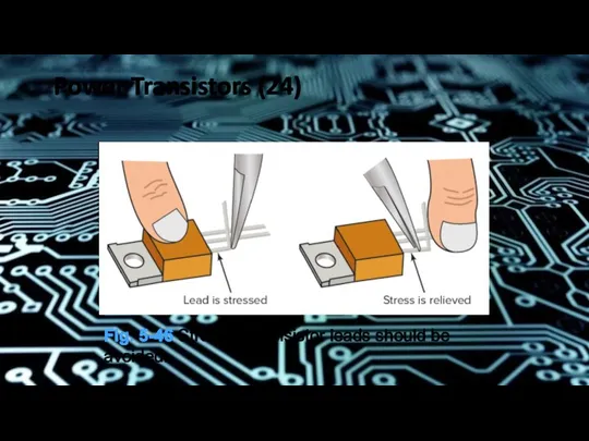
- 107. Power Transistors (23) The handling of power devices is also important. Figure 5-46 shows that lead
- 108. Power Transistors (24) Fig. 5-46 Stressing transistor leads should be avoided.
- 109. Transistors as Switches The term “solid-state switch” refers to a switch that has no moving parts.
- 110. Fig. 5-47 Computer-controlled battery conditioner
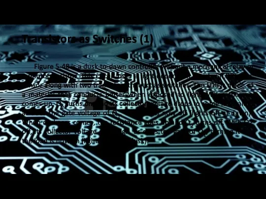
- 111. Transistors as Switches (1) Figure 5-48 is a dusk-to-dawn controller without a mechanical relay or a
- 112. Fig. 5-48 Dusk-to-dawn control circuit.
- 113. Transistors as Switches (2) Figure 5-49 is another on-off controller but this one is controlled by
- 114. Fig. 5-49 Push button control.
- 115. Transistors as Switches (3) Figure 5-50 shows another application for transistor switches. Stepper motors can be
- 116. Transistors as Switches (4) A computer or a microprocessor sends precisely timed waveforms to the switching
- 117. Fig. 5-50(a) Control of stepper motors.
- 118. Fig. 5-50(b-d) Control of stepper motors.
- 119. Transistors as Switches (5) Figure 5-51 shows control of a dc motor. The circuit achieves on-off
- 120. Fig. 5-51 Control of a dc motor.
- 121. Transistors as Switches (6) So far, the transistor switches discussed have been used for turning loads
- 122. Transistors as Switches (7) The signal source is connected to the source terminal, and the drain
- 123. Fig. 5-52 MOSFET analog switch.
- 124. Fig. 5-53 Simulated analog switch waveforms.
- 125. Summary 1. Gain is the basic function of any amplifier. 2. Gain can be calculated using
- 126. Summary (1) 8. The schematic symbol of an NPN transistor shows the emitter lead arrow Not
- 127. Summary (2) 13. Base current controls collector current and emitter current. 14. Emitters of PNP transistors
- 128. Summary (3) 20. Silicon transistors are much more widely used than germanium transistors. 21. Substitution guides
- 129. Summary (4) 26. Leakage current ICEO is β times larger than ICBO. 27. Phototransistors are biased
- 130. Summary (5) 34. An enhancement-mode MOSFET is a normally off device. It is turned on by
- 131. Summary (6) 39. Transistors that are controlled by light are useful for applications such as dusk-to-dawn
- 132. Summary (7) 43. Ideally, switching is very efficient since an open switch shows no current for
- 134. Скачать презентацию

Introduction
This lecture introduces the transistor. Transistors are solid-state devices similar
Introduction
This lecture introduces the transistor. Transistors are solid-state devices similar

Amplification
Amplification is one of the most basic ideas in electronics.
Amplification
Amplification is one of the most basic ideas in electronics.
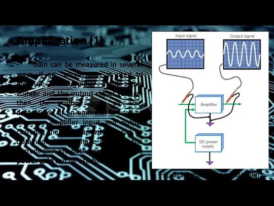
Amplification (1)
Fig. 5-1 Amplifiers provide gain.
Gain can be measured
Amplification (1)
Fig. 5-1 Amplifiers provide gain.
Gain can be measured
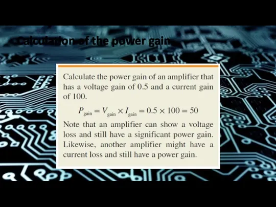
Calculation of the power gain
Calculation of the power gain
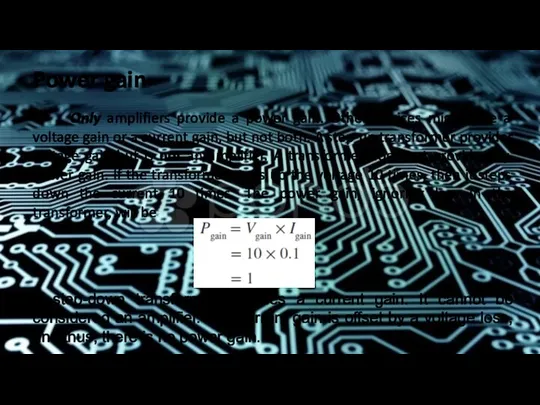
Power gain
Only amplifiers provide a power gain. Other devices might
Power gain
Only amplifiers provide a power gain. Other devices might

Amplification (2)
Even though power gain seems to be the important
Amplification (2)
Even though power gain seems to be the important
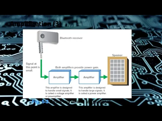
Amplification (3)
Fig. 5-2 Small-signal and large-signal amplifiers.
Amplification (3)
Fig. 5-2 Small-signal and large-signal amplifiers.
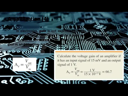
Amplification (4)
In electronics, gain is not expressed in volts, amperes,
Amplification (4)
In electronics, gain is not expressed in volts, amperes,

Transistors
Transistors provide the power gain that is needed for most
Transistors
Transistors provide the power gain that is needed for most
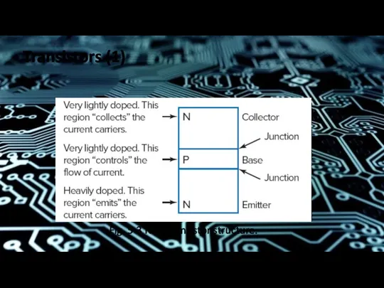
Transistors (1)
Fig. 5-3 NPN transistor structure.
Transistors (1)
Fig. 5-3 NPN transistor structure.

Transistors (2)
The transistor regions shown in Fig. 5-3 are
Transistors (2)
The transistor regions shown in Fig. 5-3 are

Transistors (3)
The transistor shown in Fig. 5-3 would be
Transistors (3)
The transistor shown in Fig. 5-3 would be
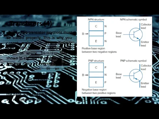
Transistors (4)
Fig. 5-4 Transistor structures and symbols.
The two transistor
Transistors (4)
Fig. 5-4 Transistor structures and symbols.
The two transistor
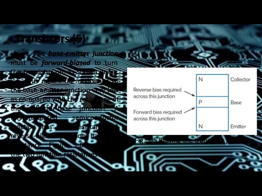
Transistors (5)
Fig. 5-5 Biasing the transistor junctions.
The base-emitter junction
Transistors (5)
Fig. 5-5 Biasing the transistor junctions.
The base-emitter junction
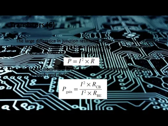
Transistors (6)
The large difference in junction resistance makes the
Transistors (6)
The large difference in junction resistance makes the
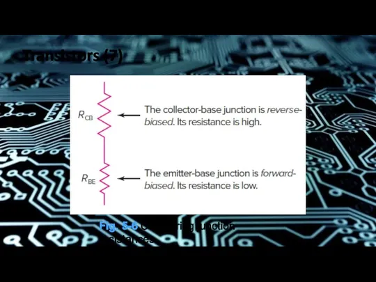
Transistors (7)
Fig. 5-6 Comparing junction resistances.
Transistors (7)
Fig. 5-6 Comparing junction resistances.
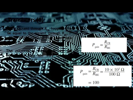
Transistors (8)
If the current through RCB happened to be equal to
Transistors (8)
If the current through RCB happened to be equal to

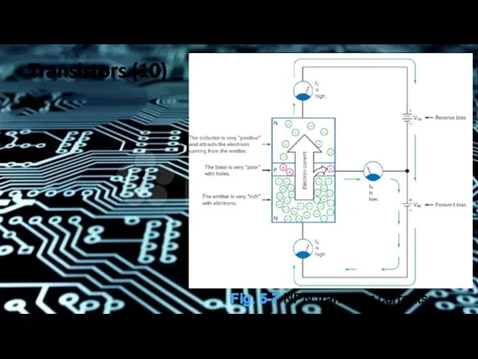
Transistors (9)
Figure 5-7 shows why the collector-base junction current is
Transistors (9)
Figure 5-7 shows why the collector-base junction current is
Transistors (10)
Fig. 5-7 NPN transistor currents.
Transistors (10)
Fig. 5-7 NPN transistor currents.

Transistors (11)
With so few electron-hole combinations in the base region,
Transistors (11)
With so few electron-hole combinations in the base region,

Transistors (12)
The current equation for Fig. 5-7 is
IE =
Transistors (12)
The current equation for Fig. 5-7 is
IE =

Transistors (13)
Current will continue to flow from the emitter to
Transistors (13)
Current will continue to flow from the emitter to
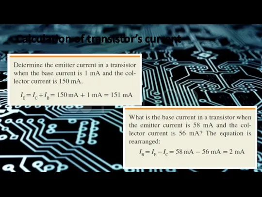
Calculation of transistor’s current
Calculation of transistor’s current
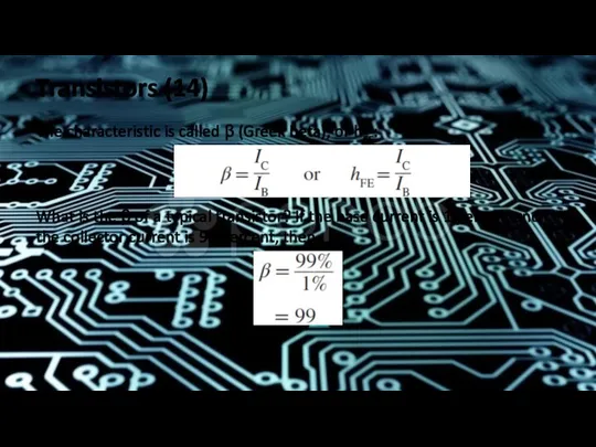
Transistors (14)
The characteristic is called β (Greek beta), or hFE:
What is
Transistors (14)
The characteristic is called β (Greek beta), or hFE:
What is
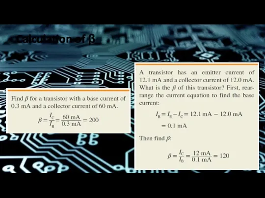
Calculation of β
Calculation of β

Transistors (15)
Figure 5-8 shows the flow from emitter to collector
Transistors (15)
Figure 5-8 shows the flow from emitter to collector
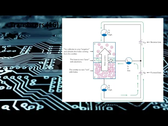
Transistors (16)
Fig. 5-8 PNP transistor currents.
Transistors (16)
Fig. 5-8 PNP transistor currents.
Characteristic Curves
As with diodes, transistor characteristic curves can provide much
Characteristic Curves
As with diodes, transistor characteristic curves can provide much
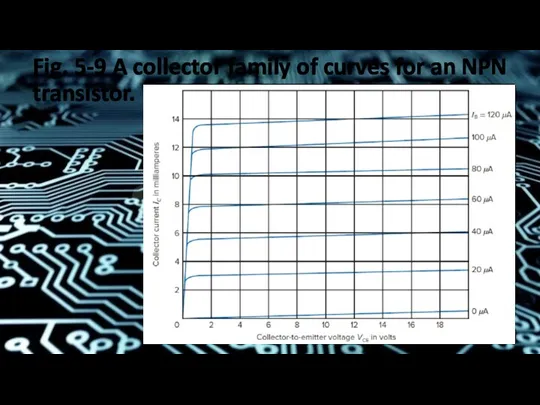
Fig. 5-9 A collector family of curves for an NPN transistor.
Fig. 5-9 A collector family of curves for an NPN transistor.
Characteristic Curves (1)
Figure 5-10 shows a circuit that can be
Characteristic Curves (1)
Figure 5-10 shows a circuit that can be
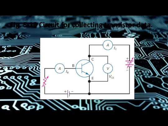
Fig. 5-10 Circuit for collecting transistor data.
Fig. 5-10 Circuit for collecting transistor data.
Characteristic Curves (2)
The variable resistor in Fig. 5-10 is adjusted
Characteristic Curves (2)
The variable resistor in Fig. 5-10 is adjusted
Characteristic Curves (3)
The two prior calculations reveal another act about
Characteristic Curves (3)
The two prior calculations reveal another act about
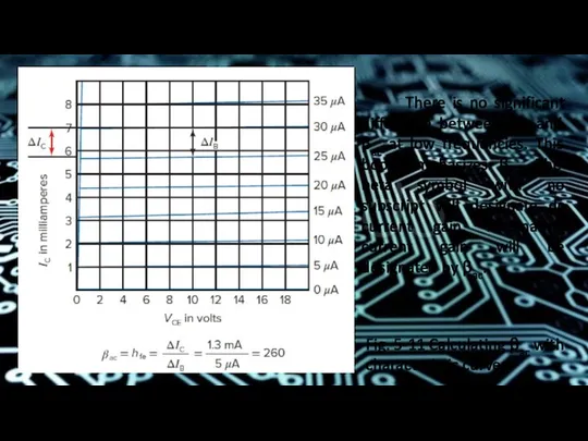
Fig. 5-11 Calculating βac with characteristic curves
There is no significant
Fig. 5-11 Calculating βac with characteristic curves
There is no significant
Transistors at high frequencies
At high frequencies the ac current gain
Transistors at high frequencies
At high frequencies the ac current gain
Characteristic Curves (4)
It is standard practice to plot positive values
Characteristic Curves (4)
It is standard practice to plot positive values
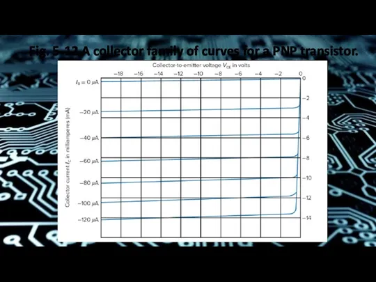
Fig. 5-12 A collector family of curves for a PNP transistor.
Fig. 5-12 A collector family of curves for a PNP transistor.
Characteristic Curves (5)
The transfer characteristic curves shown in Fig. 5-13
Characteristic Curves (5)
The transfer characteristic curves shown in Fig. 5-13
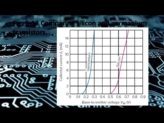
Fig. 5-13 Comparing silicon and germanium transistors.
Fig. 5-13 Comparing silicon and germanium transistors.

Transistor Data
Transistor manufacturers prepare data sheets that detail the mechanical,
Transistor Data
Transistor manufacturers prepare data sheets that detail the mechanical,

Transistor Data (1)
Comparing two transistors often shows that they are
Transistor Data (1)
Comparing two transistors often shows that they are

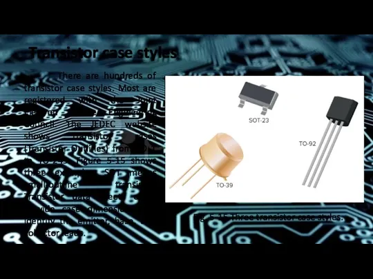
Transistor case styles
There are hundreds of transistor case styles. Most
Transistor case styles
There are hundreds of transistor case styles. Most

Transistor replacement
In some cases the part number cannot be found
Transistor replacement
In some cases the part number cannot be found
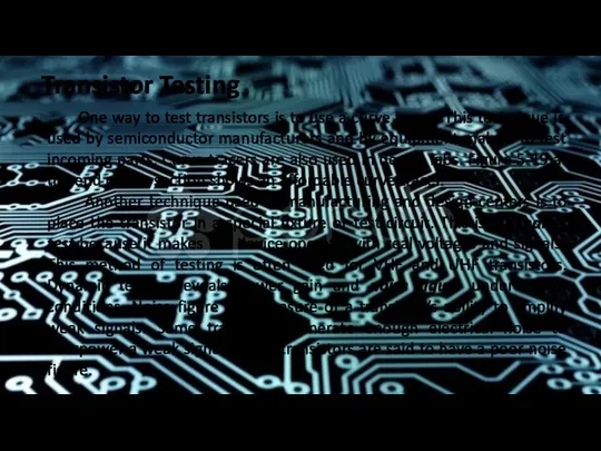
Transistor Testing
One way to test transistors is to use a
Transistor Testing
One way to test transistors is to use a
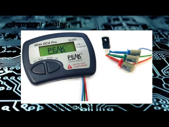
Transistor Testing
Fig. 5-19(a) Atlas DCA Pro curve tracer
Transistor Testing
Fig. 5-19(a) Atlas DCA Pro curve tracer
Transistor Testing
Fig. 5-19(b) Atlas DCA Pro curve analyzer
Transistor Testing
Fig. 5-19(b) Atlas DCA Pro curve analyzer
Transistor Testing (1)
A few transistor types may show a gradual
Transistor Testing (1)
A few transistor types may show a gradual

Transistor Testing (2)
A good transistor has two PN junctions. Both
Transistor Testing (2)
A good transistor has two PN junctions. Both

Transistor Testing (3)
The resistor will be used to provide the
Transistor Testing (3)
The resistor will be used to provide the
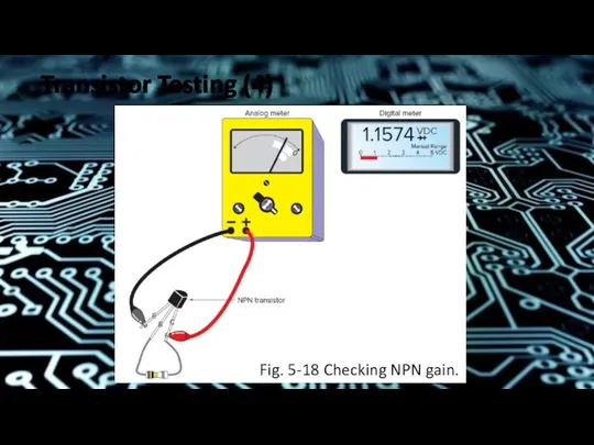
Transistor Testing (4)
Fig. 5-18 Checking NPN gain.
Transistor Testing (4)
Fig. 5-18 Checking NPN gain.
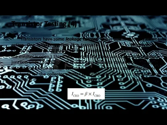
Transistor Testing (4)
Transistors have some leakage current. This is due
Transistor Testing (4)
Transistors have some leakage current. This is due
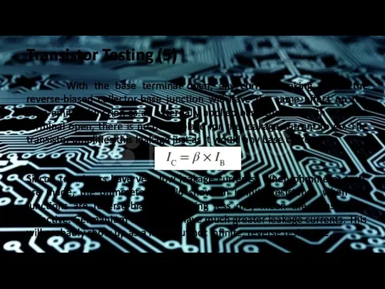
Transistor Testing (5)
With the base terminal open, any current leaking
Transistor Testing (5)
With the base terminal open, any current leaking

Other Transistor Types
Bipolar transistors use both holes and electrons as
Other Transistor Types
Bipolar transistors use both holes and electrons as
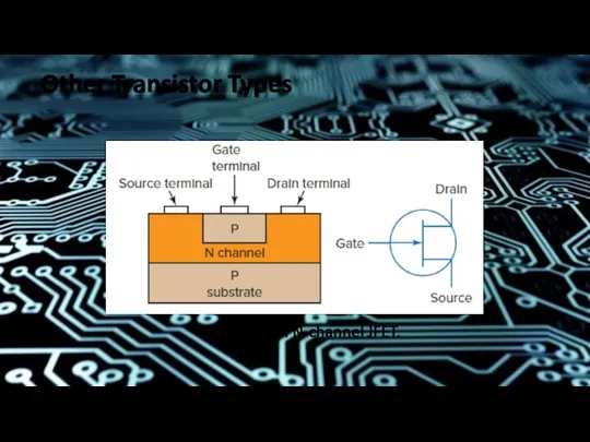
Other Transistor Types
Fig. 5-20 An N-channel JFET.
Other Transistor Types
Fig. 5-20 An N-channel JFET.
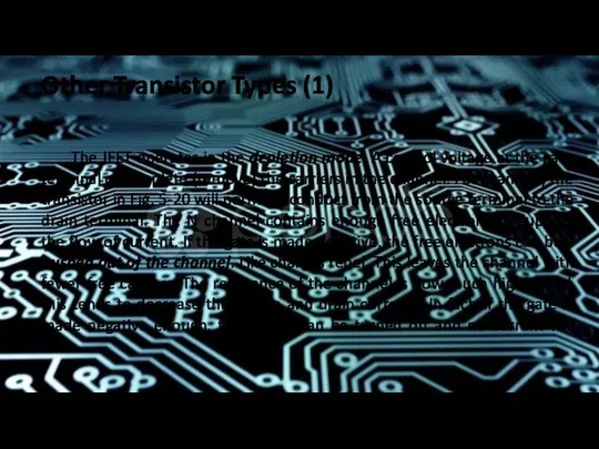
Other Transistor Types (1)
The JFET operates in the depletion mode.
Other Transistor Types (1)
The JFET operates in the depletion mode.

Other Transistor Types (2)
Examine the curves of Fig. 5-21. Notice
Other Transistor Types (2)
Examine the curves of Fig. 5-21. Notice
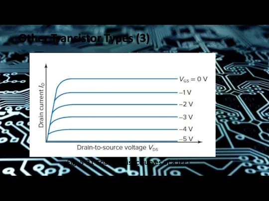
Other Transistor Types (3)
Fig. 5-21 Characteristic curves of a JFET.
Other Transistor Types (3)
Fig. 5-21 Characteristic curves of a JFET.
Other Transistor Types (4)
These are important differences: (1) The bipolar
Other Transistor Types (4)
These are important differences: (1) The bipolar

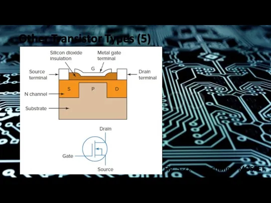
Other Transistor Types (5)
Field-effect transistors (FETs) do not require any
Other Transistor Types (5)
Field-effect transistors (FETs) do not require any
Other Transistor Types (5)
Fig. 5-22 An N-channel MOSFET.
Other Transistor Types (5)
Fig. 5-22 An N-channel MOSFET.
Other Transistor Types (6)
Early MOSFETs were very delicate. The thin
Other Transistor Types (6)
Early MOSFETs were very delicate. The thin
Other Transistor Types (7)
The gate voltage in a MOSFET circuit
Other Transistor Types (7)
The gate voltage in a MOSFET circuit

Other Transistor Types (8)
Figure 5-23 shows a family of curves
Other Transistor Types (8)
Figure 5-23 shows a family of curves
Other Transistor Types (9)
Fig. 5-23 Enhancement-mode characteristic curves.
Other Transistor Types (9)
Fig. 5-23 Enhancement-mode characteristic curves.
Other Transistor Types (10)
Figure 5-24 shows a transistor family tree.
Other Transistor Types (10)
Figure 5-24 shows a transistor family tree.
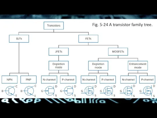
Fig. 5-24 A transistor family tree.
Fig. 5-24 A transistor family tree.

Phototransistors
What if a transistor could be controlled by something else?
Phototransistors
What if a transistor could be controlled by something else?
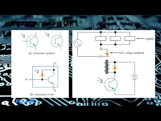
Phototransistors (1)
Fig. 5-25 Phototransistors.
Fig. 5-26 Phototransistor-controlled lighting.
Phototransistors (1)
Fig. 5-25 Phototransistors.
Fig. 5-26 Phototransistor-controlled lighting.

Phototransistors (2)
The collector is several volts positive with respect to
Phototransistors (2)
The collector is several volts positive with respect to
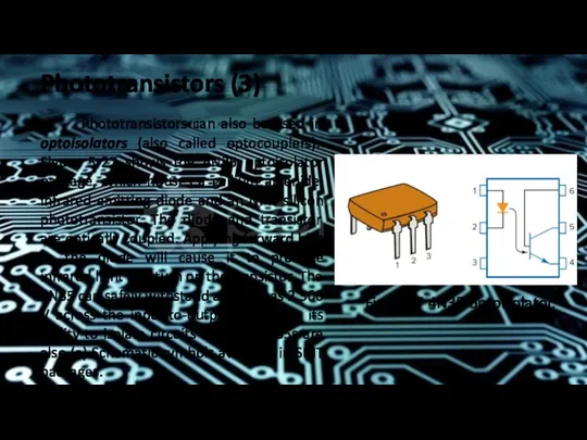
Phototransistors (3)
Phototransistors can also be used in optoisolators (also called
Phototransistors (3)
Phototransistors can also be used in optoisolators (also called
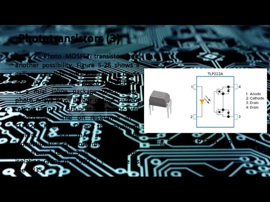
Phototransistors (3)
Photo MOSFET transistors are another possibility. Figure 5-28 shows
Phototransistors (3)
Photo MOSFET transistors are another possibility. Figure 5-28 shows

Power Transistors
Transistors can be divided into two broad categories: small-signal
Power Transistors
Transistors can be divided into two broad categories: small-signal

Power Transistors (1)
A 2N2222A conducting 200 mA and dropping 9
Power Transistors (1)
A 2N2222A conducting 200 mA and dropping 9

Power Transistors (2)
Figure 5-29 shows that there is a significant
Power Transistors (2)
Figure 5-29 shows that there is a significant
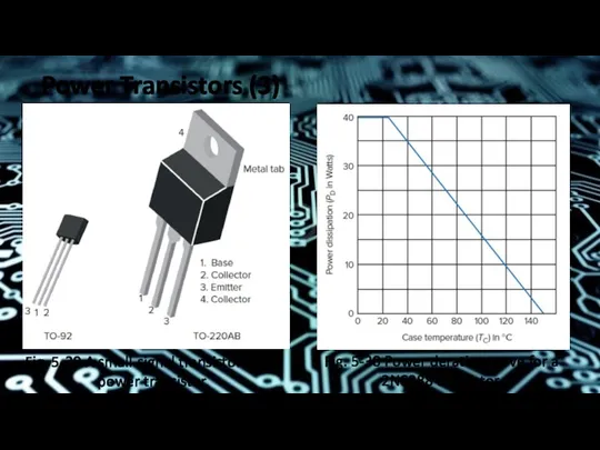
Power Transistors (3)
Fig. 5-29 A small-signal transistor and a power transistor.
Fig.
Power Transistors (3)
Fig. 5-29 A small-signal transistor and a power transistor.
Fig.
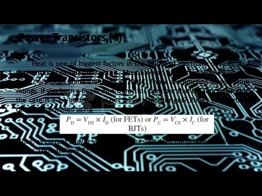
Power Transistors (4)
Heat is one of biggest factors in the
Power Transistors (4)
Heat is one of biggest factors in the
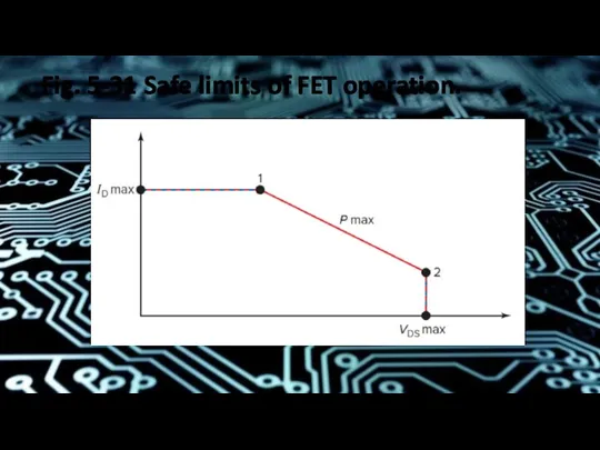
Fig. 5-31 Safe limits of FET operation.
Fig. 5-31 Safe limits of FET operation.

Power Transistors (5)
The most obvious limits are the maximum safe
Power Transistors (5)
The most obvious limits are the maximum safe
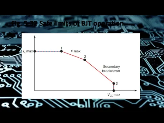
Fig. 5-32 Safe limits of BJT operation.
Fig. 5-32 Safe limits of BJT operation.

Power Transistors (6)
Notice the curve between points 2 and 3.
Power Transistors (6)
Notice the curve between points 2 and 3.
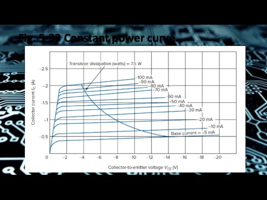
Fig. 5-33 Constant power curve.
Fig. 5-33 Constant power curve.

Power Transistors (7)
If the collector characteristic curves are extended to
Power Transistors (7)
If the collector characteristic curves are extended to
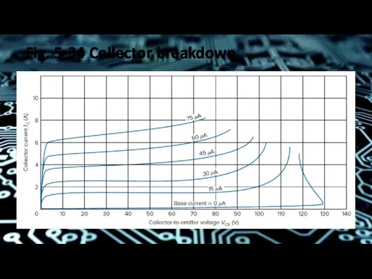
Fig. 5-34 Collector breakdown.
Fig. 5-34 Collector breakdown.
Power Transistors (8)
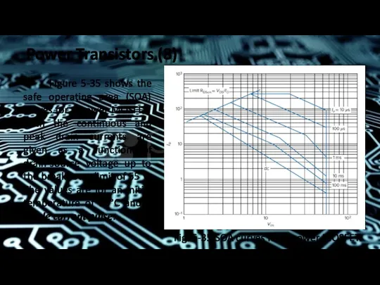
Figure 5-35 shows the safe operating area (SOA)
Power Transistors (8)
Figure 5-35 shows the safe operating area (SOA)
Power Transistors (9)
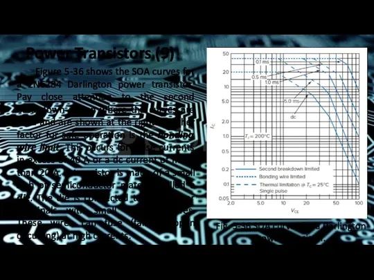
Figure 5-36 shows the SOA curves for a
Power Transistors (9)
Figure 5-36 shows the SOA curves for a

Power Transistors (10)
Figure 5-37 shows the internal circuit for a
Power Transistors (10)
Figure 5-37 shows the internal circuit for a
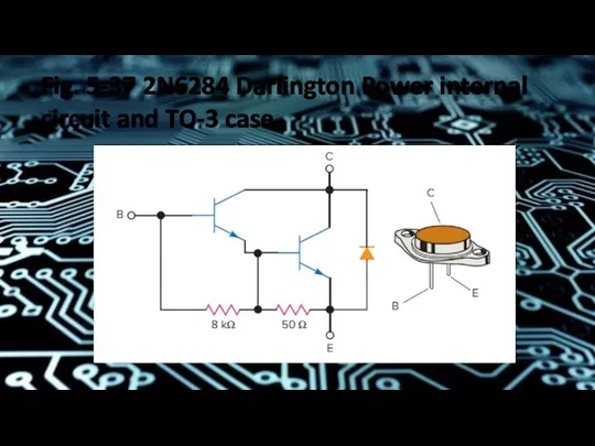
Fig. 5-37 2N6284 Darlington Power internal circuit and TO-3 case.
Fig. 5-37 2N6284 Darlington Power internal circuit and TO-3 case.

Power Transistors (11)
In addition to extra components being placed inside
Power Transistors (11)
In addition to extra components being placed inside
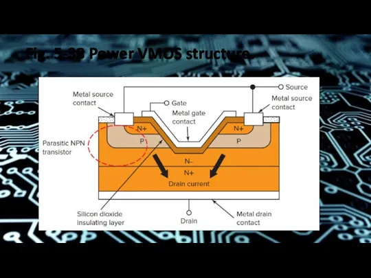
Fig. 5-38 Power VMOS structure.
Fig. 5-38 Power VMOS structure.

Power Transistors (12)
Figure 5-39 shows the schematic symbol for the
Power Transistors (12)
Figure 5-39 shows the schematic symbol for the
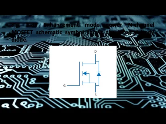
Fig. 5-39 Enhancement mode power N-channel MOSFET schematic symbol shows the
Fig. 5-39 Enhancement mode power N-channel MOSFET schematic symbol shows the

Power Transistors (13)
Figure 5-40 shows the VDS versus ID characteristic
Power Transistors (13)
Figure 5-40 shows the VDS versus ID characteristic
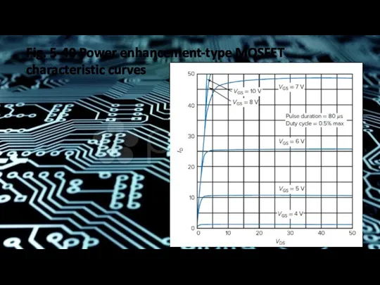
Fig. 5-40 Power enhancement-type MOSFET characteristic curves
Fig. 5-40 Power enhancement-type MOSFET characteristic curves
Power Transistors (14)
With high-power transistors, the drive requirements become important.
Power Transistors (14)
With high-power transistors, the drive requirements become important.

Power Transistors (15)
Yet another advantage of MOSFETs is that they
Power Transistors (15)
Yet another advantage of MOSFETs is that they
Power Transistors (16)
The insulated gate bipolar transistor (IGBT) is yet
Power Transistors (16)
The insulated gate bipolar transistor (IGBT) is yet
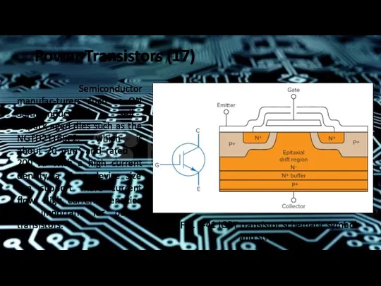
Power Transistors (17)
Semiconductor manufac-turers such as ON SemiconductorTM sell unpack-aged
Power Transistors (17)
Semiconductor manufac-turers such as ON SemiconductorTM sell unpack-aged
Power Transistors (18)
Figure 5-42 shows the saturation curves and the
Power Transistors (18)
Figure 5-42 shows the saturation curves and the
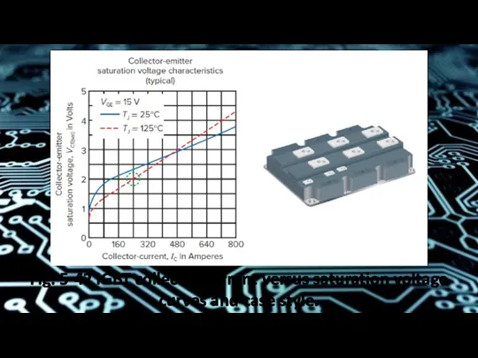
Fig. 5-42 IGBT collector current versus saturation voltage curves and case
Fig. 5-42 IGBT collector current versus saturation voltage curves and case
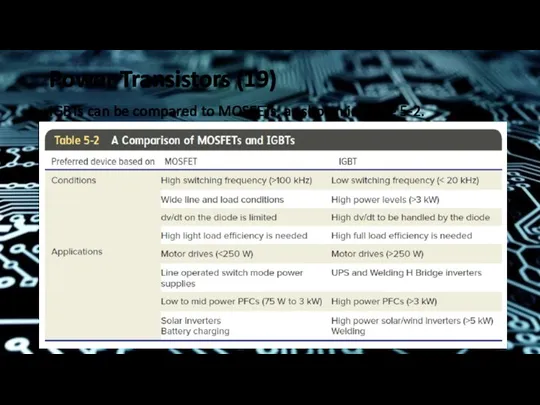
Power Transistors (19)
IGBTs can be compared to MOSFETs, as shown in
Power Transistors (19)
IGBTs can be compared to MOSFETs, as shown in
Power Transistors (20)
The thermal model of a transistor is shown
Power Transistors (20)
The thermal model of a transistor is shown
Power Transistors (21)
Designers may have to choose a large metal
Power Transistors (21)
Designers may have to choose a large metal
Power Transistors (22)
The thermal model shown in Fig. 5-43 also
Power Transistors (22)
The thermal model shown in Fig. 5-43 also
Power Transistors (23)
The handling of power devices is also important.
Power Transistors (23)
The handling of power devices is also important.
Power Transistors (24)
Fig. 5-46 Stressing transistor leads should be avoided.
Power Transistors (24)
Fig. 5-46 Stressing transistor leads should be avoided.

Transistors as Switches
The term “solid-state switch” refers to a switch
Transistors as Switches
The term “solid-state switch” refers to a switch
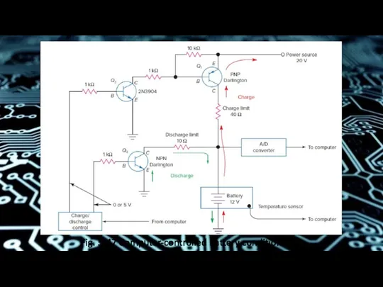
Fig. 5-47 Computer-controlled battery conditioner
Fig. 5-47 Computer-controlled battery conditioner
Transistors as Switches (1)
Figure 5-48 is a dusk-to-dawn controller without
Transistors as Switches (1)
Figure 5-48 is a dusk-to-dawn controller without
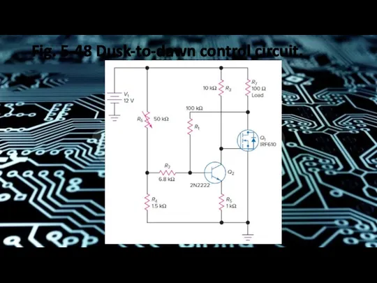
Fig. 5-48 Dusk-to-dawn control circuit.
Fig. 5-48 Dusk-to-dawn control circuit.

Transistors as Switches (2)
Figure 5-49 is another on-off controller but
Transistors as Switches (2)
Figure 5-49 is another on-off controller but
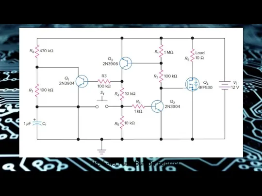
Fig. 5-49 Push button control.
Fig. 5-49 Push button control.
Transistors as Switches (3)
Figure 5-50 shows another application for transistor
Transistors as Switches (3)
Figure 5-50 shows another application for transistor
Transistors as Switches (4)
A computer or a microprocessor sends precisely
Transistors as Switches (4)
A computer or a microprocessor sends precisely
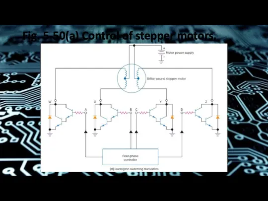
Fig. 5-50(a) Control of stepper motors.
Fig. 5-50(a) Control of stepper motors.
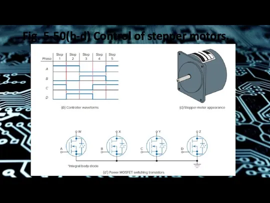
Fig. 5-50(b-d) Control of stepper motors.
Fig. 5-50(b-d) Control of stepper motors.

Transistors as Switches (5)
Figure 5-51 shows control of a dc
Transistors as Switches (5)
Figure 5-51 shows control of a dc
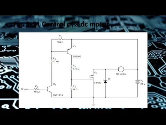
Fig. 5-51 Control of a dc motor.
Fig. 5-51 Control of a dc motor.
Transistors as Switches (6)
So far, the transistor switches discussed have
Transistors as Switches (6)
So far, the transistor switches discussed have
Transistors as Switches (7)
The signal source is connected to the
Transistors as Switches (7)
The signal source is connected to the
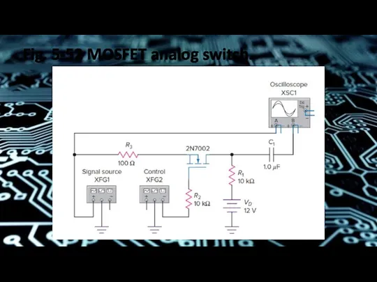
Fig. 5-52 MOSFET analog switch.
Fig. 5-52 MOSFET analog switch.
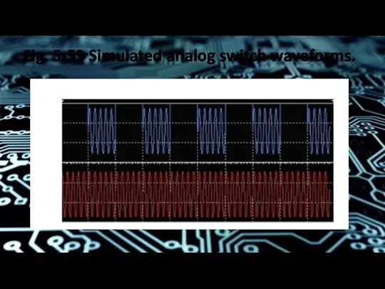
Fig. 5-53 Simulated analog switch waveforms.
Fig. 5-53 Simulated analog switch waveforms.

Summary
1. Gain is the basic function of any amplifier.
2. Gain can
Summary
1. Gain is the basic function of any amplifier.
2. Gain can

Summary (1)
8. The schematic symbol of an NPN transistor shows the
Summary (1)
8. The schematic symbol of an NPN transistor shows the
Summary (2)
13. Base current controls collector current and emitter current.
14. Emitters
Summary (2)
13. Base current controls collector current and emitter current.
14. Emitters

Summary (3)
20. Silicon transistors are much more widely used than germanium
Summary (3)
20. Silicon transistors are much more widely used than germanium

Summary (4)
26. Leakage current ICEO is β times larger than ICBO.
27.
Summary (4)
26. Leakage current ICEO is β times larger than ICBO.
27.

Summary (5)
34. An enhancement-mode MOSFET is a normally off device. It
Summary (5)
34. An enhancement-mode MOSFET is a normally off device. It

Summary (6)
39. Transistors that are controlled by light are useful for
Summary (6)
39. Transistors that are controlled by light are useful for

Summary (7)
43. Ideally, switching is very efficient since an open switch
Summary (7)
43. Ideally, switching is very efficient since an open switch
 Биография А.С. Пушкина Диск
 Русская народная сказка Репка
 Устройства приема и преобразования сигналов (УП и ПС)
 Нормы времени на погрузку и разгрузку транспортных средств
 Кафедра физического воспитания и спорта РАНХиГС
 Исполнительная власть в Российской Федерации
 Тез кескіш болаттар
 Создание штаммов микроорганизмов для биотехнологии
 Поняття текстового документа, його об’єктів. Урок 18
 Географическая карта.Урок географии в 5 классе
 Подготовка данных к анализу. (Лекция 5)
 Путешествие по стране Информация. Измерение информации
 Обзор книги Сила воли. Автор: Келли Макгонигал
 Шаблон презентации
 Классный час по теме Символика современных олимпийских игр.
 Забавные животные
 Шаблоны презентаций по математике
 Защита от воздействия высоких и низких температур
 Электрический чайник
 Будущие избиратели
 Дециметр (дм)
 Сценарий для пришкольного лагеря с презентацией До-Ми-Соль-ка
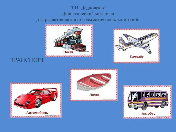 Дидактический материалдля развития лексико-грамматических категорий. Транспорт.
 Нефть и газ. Химический состав и свойства
 Классный час на тему Человек отражается в своих поступках
 Симптомы и методы обследования в пульмонологии
 Кондитерская фабрика Красный Октябрь. Товарищество Эйнем в Москве
 Архитектура России в начале XIX века