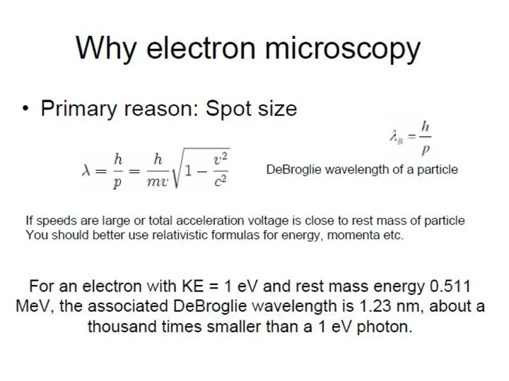
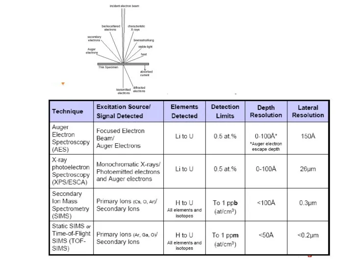
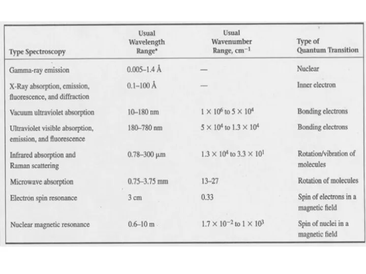
- Basics Material Characterization Techniques. Structural (bulk and surface) Optical

Содержание
- 2. Basic Electron Microscopy
- 4. Electron Microscopy - definition and types Developed in the 1930s that use electron beams instead of
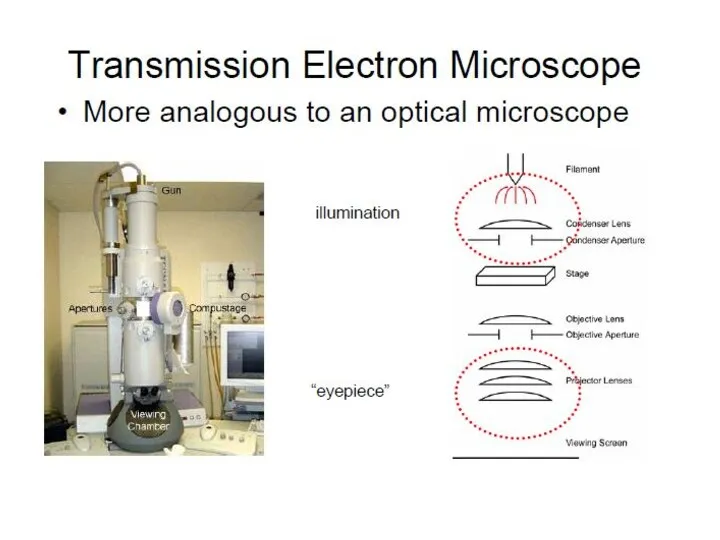
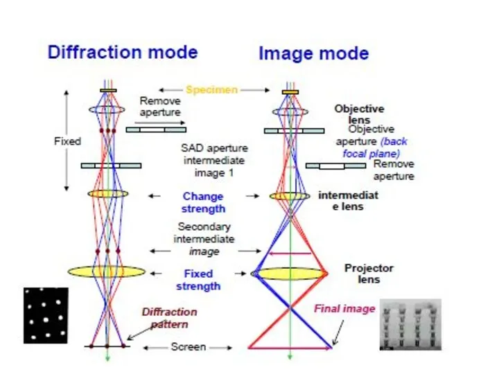
- 5. Transmission Electron Microscopy (TEM) beam of electronsbeam of electrons is transmitted through a specimen, then an
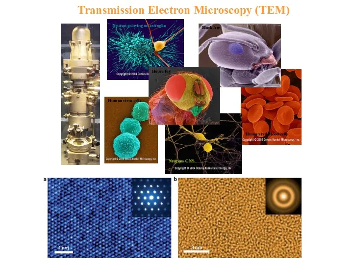
- 6. Transmission Electron Microscopy (TEM) Black Ant House Fly Human red blood cells Human stem cells Neurons
- 7. type of electron microscope capable of producing high-resolution images of a sample surface. due to the
- 8. the electron gun
- 12. Identify Elements by EELS (Electron Energy Loss Spectroscopy) An element can be identified by its characteristic
- 13. Identify Elements by EDX (Energy-Dispersive X-ray Analysis) Identify an element by its core level fluorescence energy.
- 15. XPS spectoscopy Photon removes a bound electron according to: KE = hν - BE - Φ
- 16. Work Function Consequence of the photoelectric effect Φ = EVAC - єF Important indicator of physical
- 17. Photoemission spectroscopy XPS UPS
- 19. Scanning Tunneling Microscope (STM) x feedback regulator high voltage amplifier z y I Negative feedback keeps
- 20. Technology Required for a STM Sharp, clean tip (Etching, ion bombardment, field desorption by pulsing) Piezo-electric
- 21. Atomic resolution, several orders of magnitude better than the best electron microscope Quantum mechanical tunnel-effect of
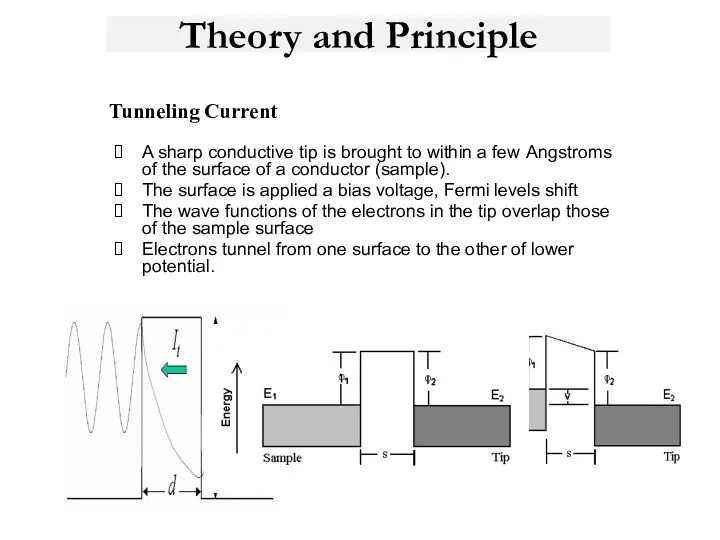
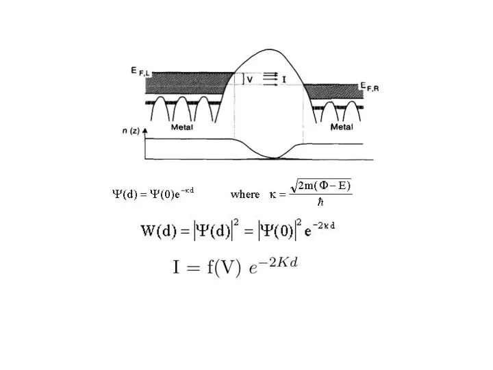
- 22. Theory and Principle A sharp conductive tip is brought to within a few Angstroms of the
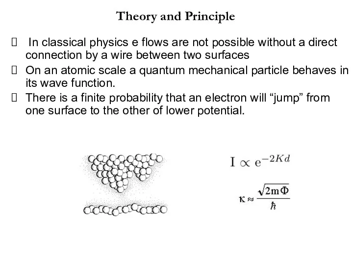
- 24. Theory and Principle In classical physics e flows are not possible without a direct connection by
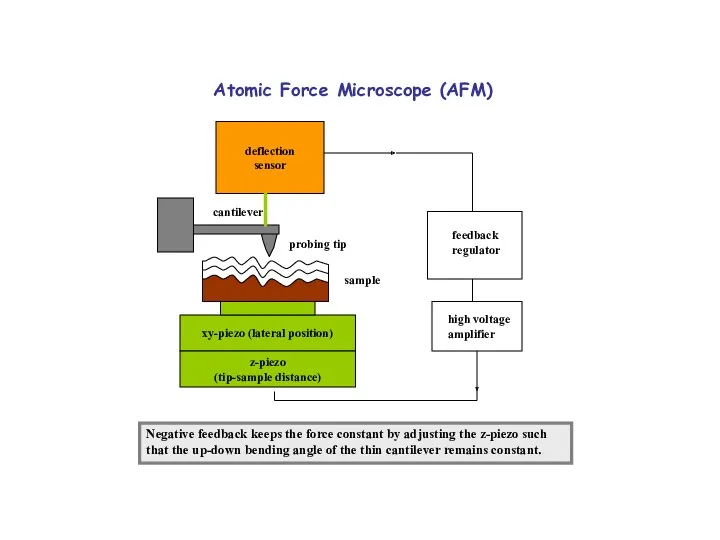
- 25. Atomic Force Microscope (AFM) sample feedback regulator high voltage amplifier xy-piezo (lateral position) deflection sensor probing
- 26. Deflection sensors Laser Photodiode with four quadrants
- 27. Beam-deflection method A light beam is reflected from the cantilever onto a photodiode divided into 4
- 28. AFM Cantilever and Tip To obtain an extra sharp AFM tip one can attach a carbon
- 29. Energy U and force F between tip and sample as a function of their distance z.
- 30. Dynamic Force Detection The cantilever oscillates like a tuning fork at resonance. Frequency shift and amplitude
- 31. STM versus AFM STM is particularly useful for probing electrons at surfaces, for example the electron
- 32. Electromagnetic Waves Maxwell’s equations
- 35. Energy Units for EM waves The Energy of EM waves is measured in several different units
- 36. UV-VIS spectroscopy
- 37. Linear spectroscopy Absorption Coefficient
- 38. Raman Spectroscopy Basics Basic Physical Realization Illuminate a specimen with laser light (e.g. 532nm) Scattered (no
- 40. Not every crystal lattice vibration can be probed by Raman scattering. There are certain Selection rules:
- 42. Example of Raman scattering in crystalline solids
- 43. far- infrared: 400-10 cm-1: 400-10 cm-1 (1000–30 μm), adjacent to the microwave: 400-10 cm-1 (1000–30 μm),
- 44. IR SPECTROSCOPY
- 45. IR vibrational spectrum for Formaldehyde
- 46. Raman vs. FTIR FTIR Sensitive to functional group vibrations especially OH stretch in water, good for
- 47. Luminescence Luminescence : Emission of radiation in excess of the amount emitted in thermal Equilibrium (Non
- 48. Photoluminescence in semiconductors
- 50. PL spectrum of a semiconductor Reduced peak width at low temperature Photoluminescence intensity is related to
- 51. Impurity Levels in semiconductors Shallow impurity Levels
- 52. Excitons Electrons and holes bound together by their Coulomb Interaction Important at low temperatures LEDs and
- 53. Interaction of Electrons, X-rays, and Neutrons with matter
- 55. Скачать презентацию
Basic Electron Microscopy
Basic Electron Microscopy
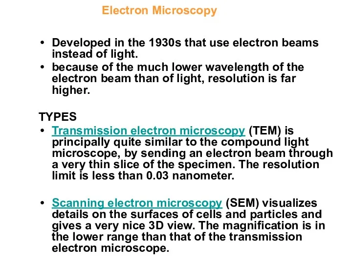
Electron Microscopy - definition and types
Developed in the 1930s that use
Electron Microscopy - definition and types
Developed in the 1930s that use
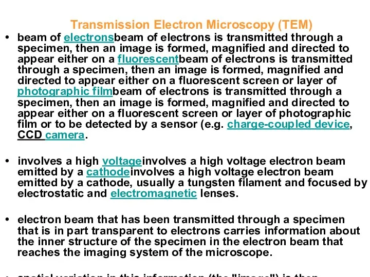
Transmission Electron Microscopy (TEM)
beam of electronsbeam of electrons is transmitted
Transmission Electron Microscopy (TEM)
beam of electronsbeam of electrons is transmitted
Transmission Electron Microscopy (TEM)
Black Ant
House Fly
Human red blood
Transmission Electron Microscopy (TEM)
Black Ant
House Fly
Human red blood
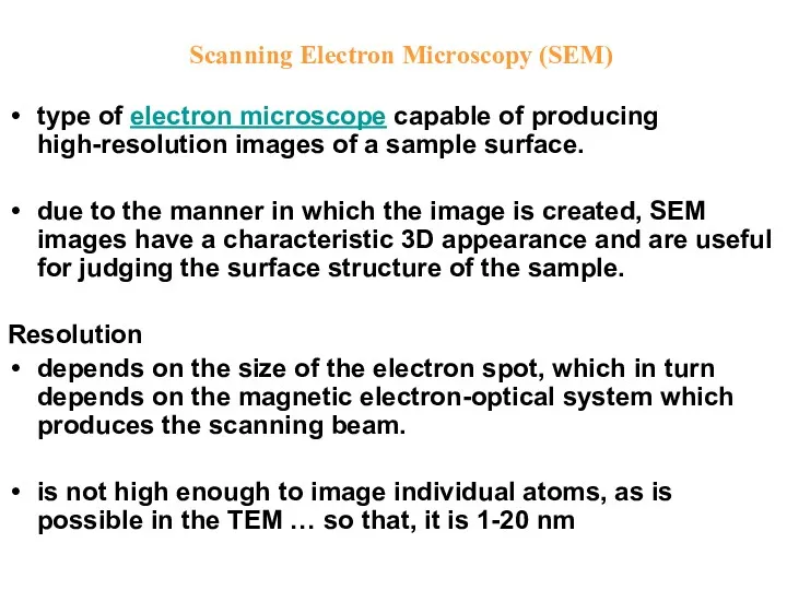
type of electron microscope capable of producing high-resolution images of a
type of electron microscope capable of producing high-resolution images of a
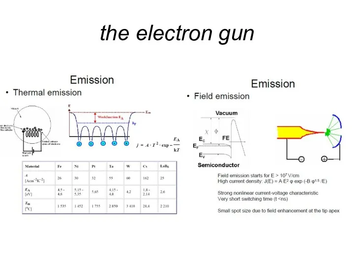
the electron gun
the electron gun
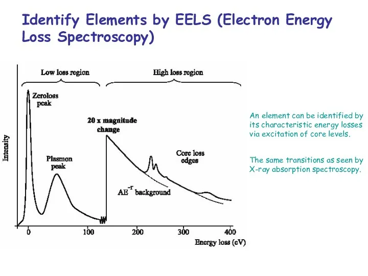
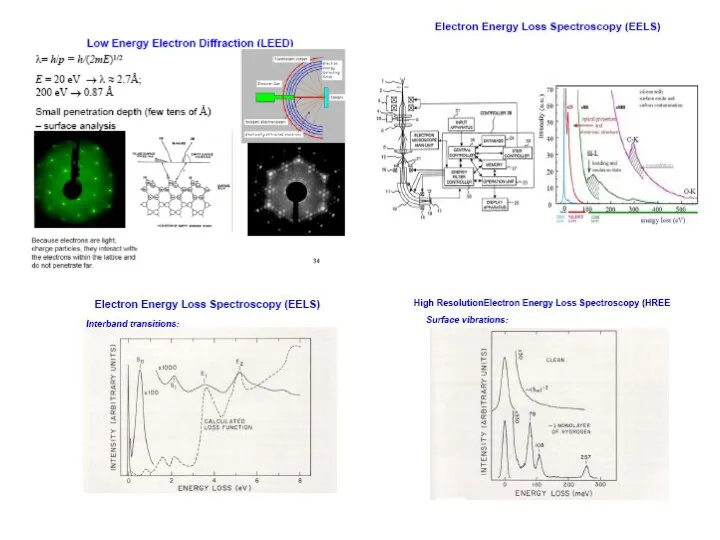
Identify Elements by EELS (Electron Energy Loss Spectroscopy)
An element can be
Identify Elements by EELS (Electron Energy Loss Spectroscopy)
An element can be
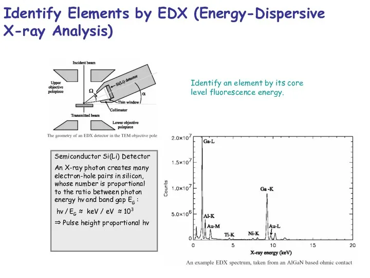
Identify Elements by EDX (Energy-Dispersive X-ray Analysis)
Identify an element by its
Identify Elements by EDX (Energy-Dispersive X-ray Analysis)
Identify an element by its
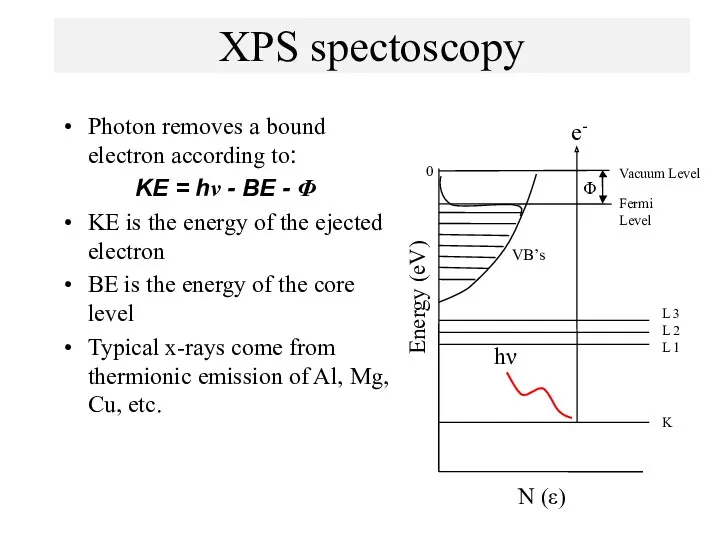
XPS spectoscopy
Photon removes a bound electron according to:
KE = hν -
XPS spectoscopy
Photon removes a bound electron according to:
KE = hν -
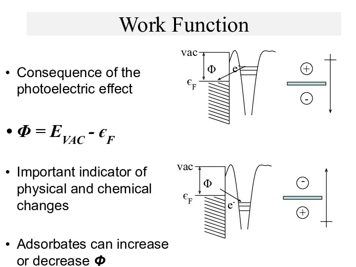
Work Function
Consequence of the photoelectric effect
Φ = EVAC - єF
Important indicator
Work Function
Consequence of the photoelectric effect
Φ = EVAC - єF
Important indicator
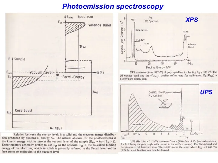
Photoemission spectroscopy
XPS
UPS
Photoemission spectroscopy
XPS
UPS
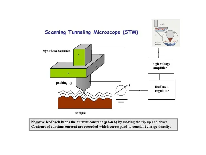
Scanning Tunneling Microscope (STM)
x
feedback
regulator
high voltage
amplifier
z
y
I
Negative feedback keeps the current constant
Scanning Tunneling Microscope (STM)
x
feedback
regulator
high voltage
amplifier
z
y
I
Negative feedback keeps the current constant
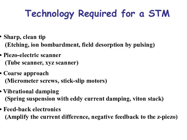
Technology Required for a STM
Sharp, clean tip
(Etching, ion
Technology Required for a STM
Sharp, clean tip (Etching, ion
Atomic resolution, several orders of magnitude better than the best electron
Atomic resolution, several orders of magnitude better than the best electron
Theory and Principle
A sharp conductive tip is brought to within a
Theory and Principle
A sharp conductive tip is brought to within a
Theory and Principle
In classical physics e flows are not possible
Theory and Principle
In classical physics e flows are not possible
Atomic Force Microscope (AFM)
sample
feedback
regulator
high voltage
amplifier
xy-piezo (lateral position)
deflection
sensor
probing tip
cantilever
z-piezo
(tip-sample distance)
Negative feedback
Atomic Force Microscope (AFM)
sample
feedback
regulator
high voltage
amplifier
xy-piezo (lateral position)
deflection
sensor
probing tip
cantilever
z-piezo
(tip-sample distance)
Negative feedback
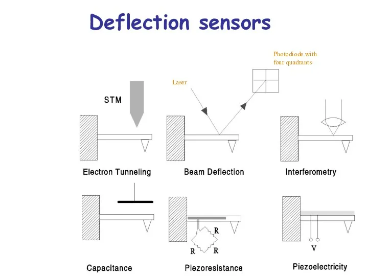
Deflection sensors
Laser
Photodiode with four quadrants
Deflection sensors
Laser
Photodiode with four quadrants
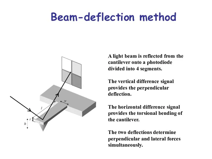
Beam-deflection method
A light beam is reflected from the cantilever onto a
Beam-deflection method
A light beam is reflected from the cantilever onto a
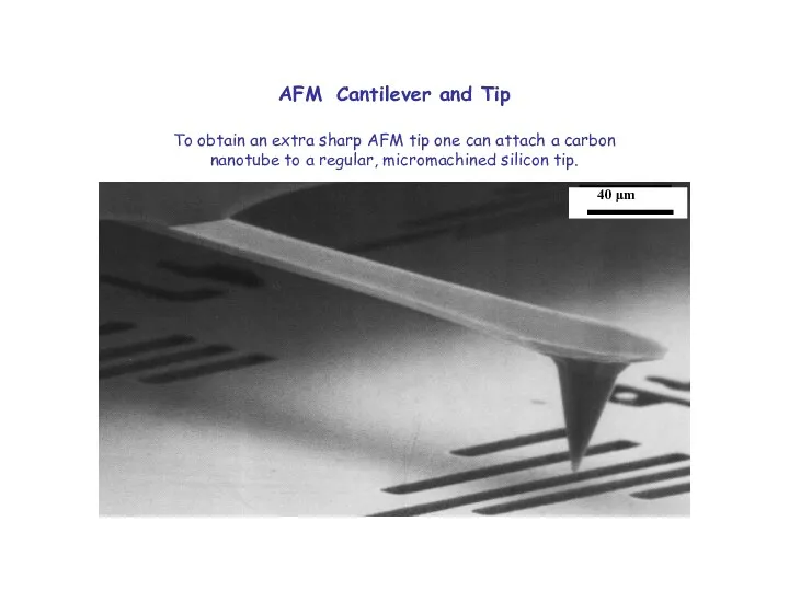
AFM Cantilever and Tip
To obtain an extra sharp AFM tip one
AFM Cantilever and Tip To obtain an extra sharp AFM tip one
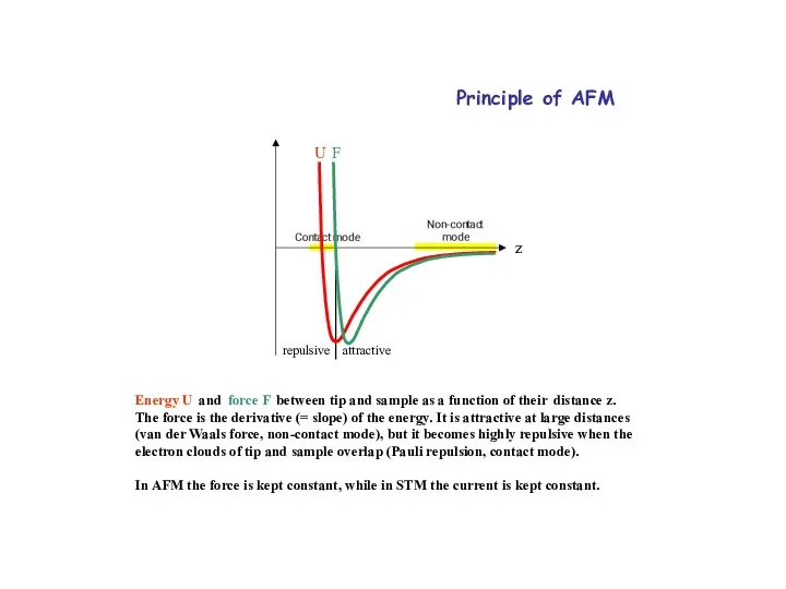
Energy U and force F between tip and sample as a
Energy U and force F between tip and sample as a
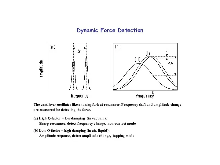
Dynamic Force Detection
The cantilever oscillates like a tuning fork at resonance.
Dynamic Force Detection
The cantilever oscillates like a tuning fork at resonance.
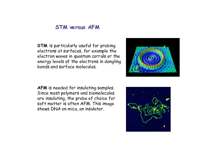
STM versus AFM
STM is particularly useful for probing electrons at surfaces,
STM versus AFM
STM is particularly useful for probing electrons at surfaces,
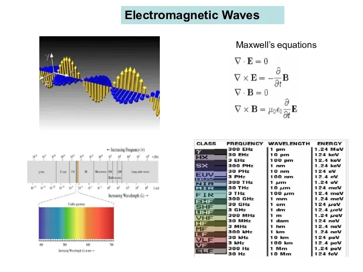
Electromagnetic Waves
Maxwell’s equations
Electromagnetic Waves
Maxwell’s equations
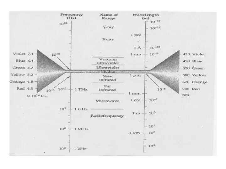
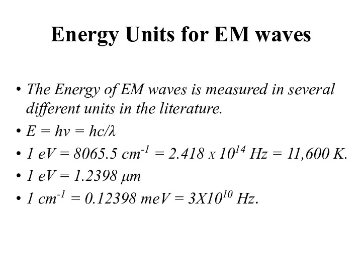
Energy Units for EM waves
The Energy of EM waves is measured
Energy Units for EM waves
The Energy of EM waves is measured
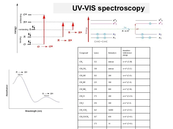
UV-VIS spectroscopy
UV-VIS spectroscopy
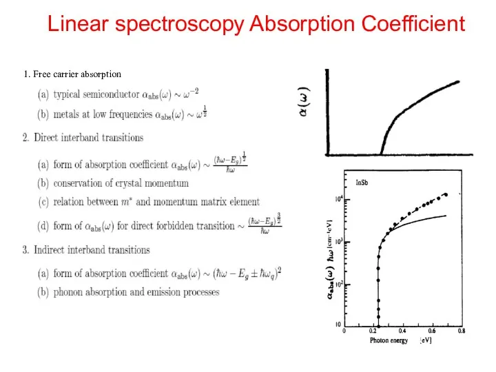
Linear spectroscopy Absorption Coefficient
Linear spectroscopy Absorption Coefficient
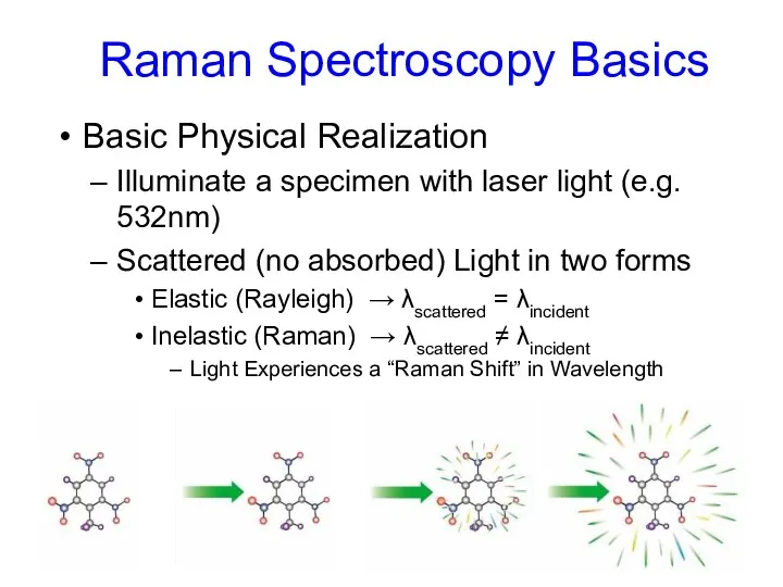
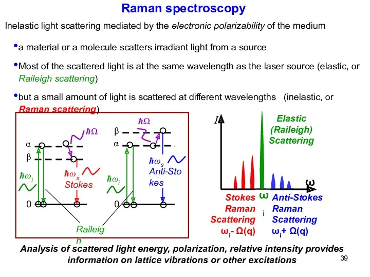
Raman Spectroscopy Basics
Basic Physical Realization
Illuminate a specimen with laser light (e.g.
Raman Spectroscopy Basics
Basic Physical Realization
Illuminate a specimen with laser light (e.g.
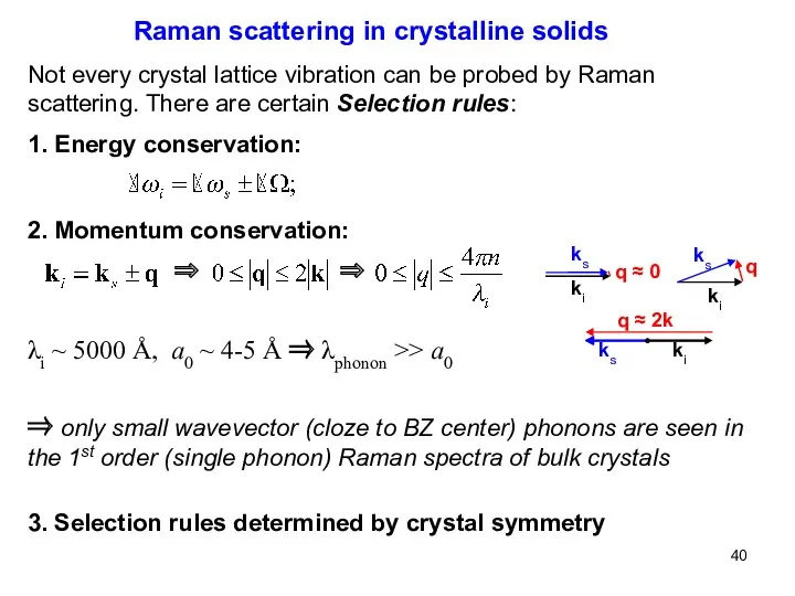
Not every crystal lattice vibration can be probed by Raman scattering.
Not every crystal lattice vibration can be probed by Raman scattering.
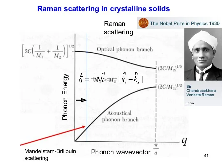
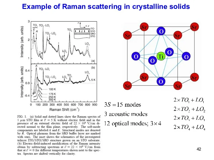
Example of Raman scattering in crystalline solids
Example of Raman scattering in crystalline solids
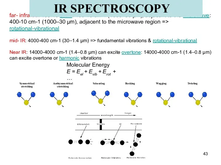
far- infrared: 400-10 cm-1: 400-10 cm-1 (1000–30 μm), adjacent to the microwave: 400-10 cm-1 (1000–30 μm),
far- infrared: 400-10 cm-1: 400-10 cm-1 (1000–30 μm), adjacent to the microwave: 400-10 cm-1 (1000–30 μm),
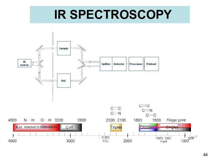
IR SPECTROSCOPY
IR SPECTROSCOPY
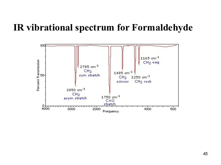
IR vibrational spectrum for Formaldehyde
IR vibrational spectrum for Formaldehyde
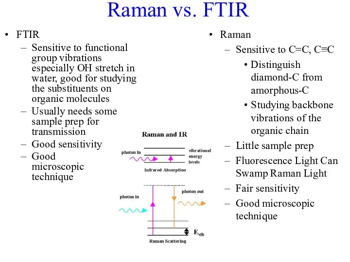
Raman vs. FTIR
FTIR
Sensitive to functional group vibrations especially OH stretch in
Raman vs. FTIR
FTIR
Sensitive to functional group vibrations especially OH stretch in
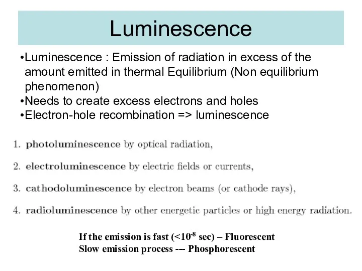
Luminescence
Luminescence : Emission of radiation in excess of the
amount emitted
Luminescence
Luminescence : Emission of radiation in excess of the
amount emitted
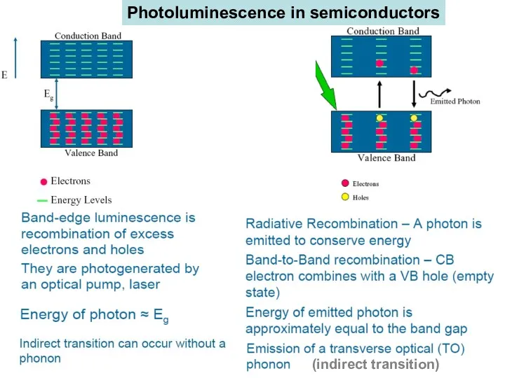
Photoluminescence in semiconductors
Photoluminescence in semiconductors
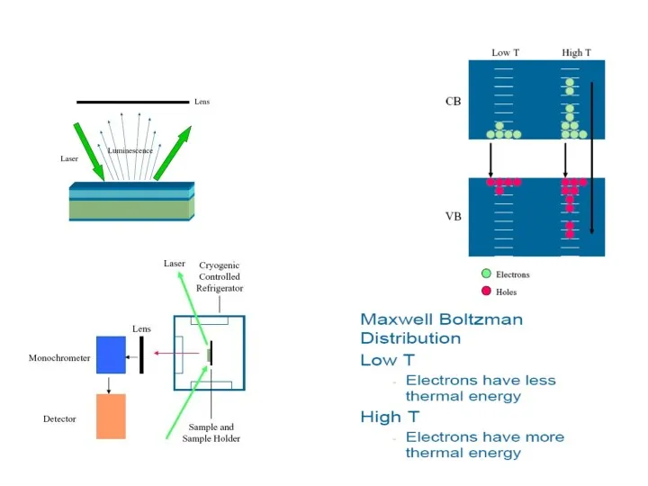
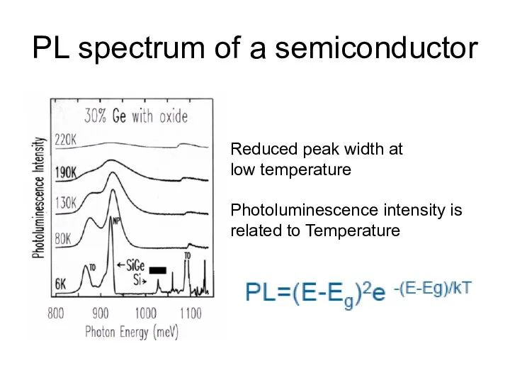
PL spectrum of a semiconductor
Reduced peak width at
low temperature
Photoluminescence intensity
PL spectrum of a semiconductor
Reduced peak width at
low temperature
Photoluminescence intensity
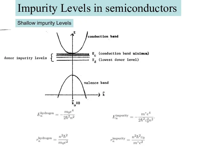
Impurity Levels in semiconductors
Shallow impurity Levels
Impurity Levels in semiconductors
Shallow impurity Levels
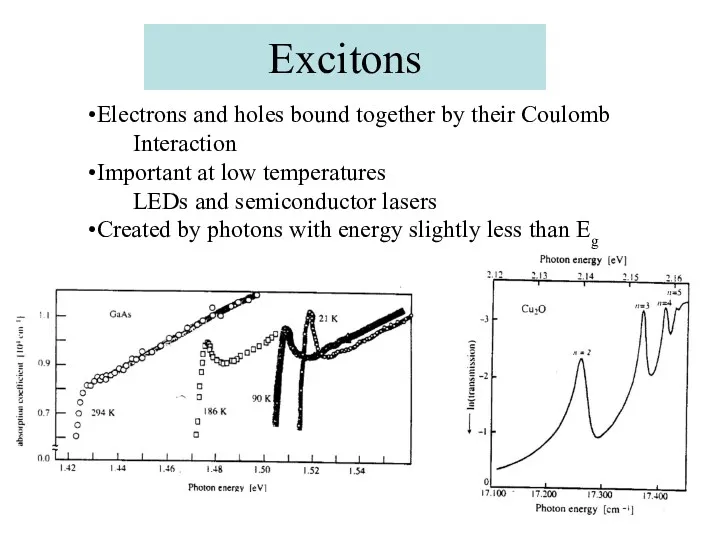
Excitons
Electrons and holes bound together by their Coulomb
Interaction
Important at low
Excitons
Electrons and holes bound together by their Coulomb
Interaction
Important at low
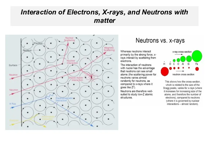
Interaction of Electrons, X-rays, and Neutrons with matter
Interaction of Electrons, X-rays, and Neutrons with matter
 History and philosophy sciences
 Pulmonary tuberculosis. The Passive Voice. Present and Past Nenses the Pfssive Voice
 The history of Russian cinema
 Mixed Conditionals
 Времена в английском языке
 Future profession. Choosing a career
 Country I want to visit is France
 My pet Tell about your pet
 How did you spend your summer holidays
 How to spend your weekend? Оutdoor activities
 Coachella Festival
 Typical houses in Britain
 Mercedes-Benz
 English - language authors
 What is the weather like today
 Your future, our future. Environment quiz
 My flat
 Funny food
 Northern Ireland
 My idol Sjostrom Sarah
 Особенности официально-делового перевода
 British english vs. american english
 Modal verbs
 My ideal school
 Books in our life
 Images of Ukraine
 Holiday travel
 Sharks