- Nano Materials Synthesis

Содержание
- 2. Length scale
- 3. Fundamental Length Scales in Physics Quantum Electric Magnetic Quantum Well: Quantum Well Laser Capacitor: Single Electron
- 4. Elastic Inelastic ΔE = 0 ΔE > 0 Scattering Potential → Electron- Electron- Trapping at Diffraction,
- 5. Screening Lengths l ~ 1 / √n (n = Density of screening charges) Metals: Semiconductors: Electrolytes:
- 6. Length Scales in Polymers (including Biopolymers, such as DNA and Proteins) Random Walk, Entropy Stiffness α
- 7. Top-down versus Bottom-up
- 8. Nucleation and Growth of Crystals
- 9. Typical precipitation reaction: Reactant 1 + Reactant 2 Product + By-product Nucleation & Growth
- 10. Nucleation and Growth Rates Control Rc Nucleation, the first step… First process is for microscopic clusters
- 11. Nucleation Rate – Thermodynamic barrier W* At r*, (∂W(r)/ ∂r)r=r* = 0 r* = -2σ/ ΔGcryst(T)
- 12. Bottom-up Approaches Two approaches thermodynamic equilibrium approach generation of supersaturation nucleation subsequent growth kinetic approach limiting
- 13. Homogeneous nucleation Liquid, vapor or solid supersaturation temperature reduction metal quantum dots in glass matrix by
- 14. Homogeneous nucleation Driving force Fig 3.1
- 15. Homogeneous nucleation Energy barrier Gibss free energy change
- 16. Nuclei formation favor: high initial concentration or supersaturation low viscosity low critical energy barrier uniform nanoparticle
- 17. Nuclei growth Steps growth species generation diffusion from bulk to the growth surface adsorption surface growth
- 18. Ostwald ripening Many small crystals form in a system initially but slowly disappear except for a
- 19. “LEEM (Low-energy electron microscopy) images of ripening of single atomic layer height islands on Si(001) at
- 20. Metallic nanoparticles Reduction of metal complexes in dilute solution Diffusion-limited process maintaining Example: nano-gold particles chlorauric
- 21. Semiconductor nanoparticles Pyrolysis of organometallic precursor(s) dissolved in anhydrate solvents at elevated temperatures in an airless
- 22. Oxide nanoparticles Several methods principles: burst of homogeneous nucleation + diffusion controlled growth most commonly: sol-gel
- 23. Sol-gel process
- 24. SOL-GEL SCIENCE Gelification Aging Soaking Mix the reactives Sol Gel Gel Aerogel Hydrolysis and Condesation Gelification
- 25. Gelification Mix reactives Sol Gel Gel Gelification Aging Hydrolysis and Condesation reactions take place
- 26. Sol-gel process Hydrolysis e.g. Condensation of precursors e.g. typical precursors: metal alkoxides or inorganic and organic
- 27. Sol-gel example: silica Precursors: silicone alkoxides with different alkyl ligand sizes catalyst: ammonia solvent: various alcohols
- 28. Heterogeneous nucleation A new phase forms on a surface of another material thermal oxidation, sputtering and
- 29. Heterogeneous nucleation
- 30. Solvothermal Synthesis
- 31. Hydrothermal Synthesis The reactants are dissolved (or placed) in water or another solvent (solvothermal) in a
- 32. Solvothermal Synthesis
- 33. Reduction in solution
- 34. Reduction in solution
- 35. Reduction in solution - How to control the particles
- 36. Reduction in solution - How to control the particles Seed-mediated growth
- 37. One dimensional nanostructures Nanowires Nanotubes “They represent the smallest dimension for efficient transport of electrons and
- 38. Synthesis Methods
- 39. Spontaneous Growth A growth driven by reduction of Gibbs free energy or chemical potential. This can
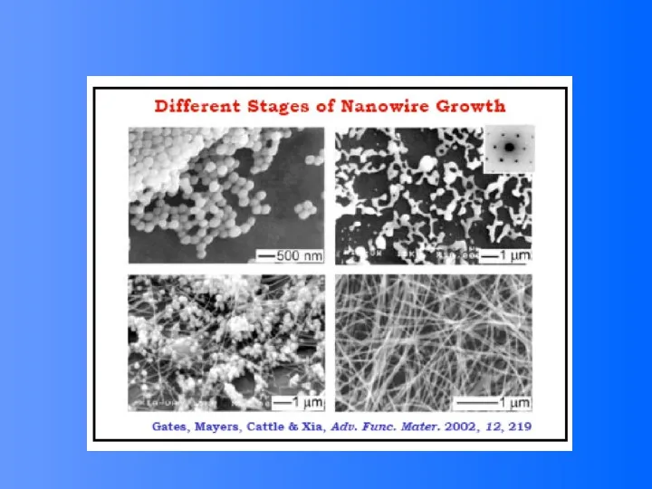
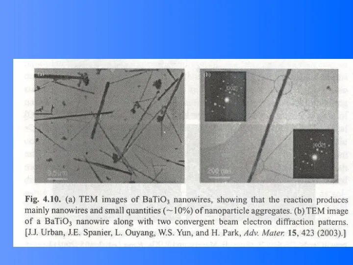
- 40. Growth of Single Crystal Nanobelts of Semiconducting or metal oxides Evaporating the metal oxides (ZnO, SnO2,
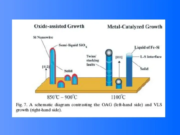
- 43. By controlling growth kinetics, a consequence of minimizing the total energy attributed by spontaneous polarization and
- 44. Dissolution and Condensation Growth The growth species first dissolve into a solvent or a solution, and
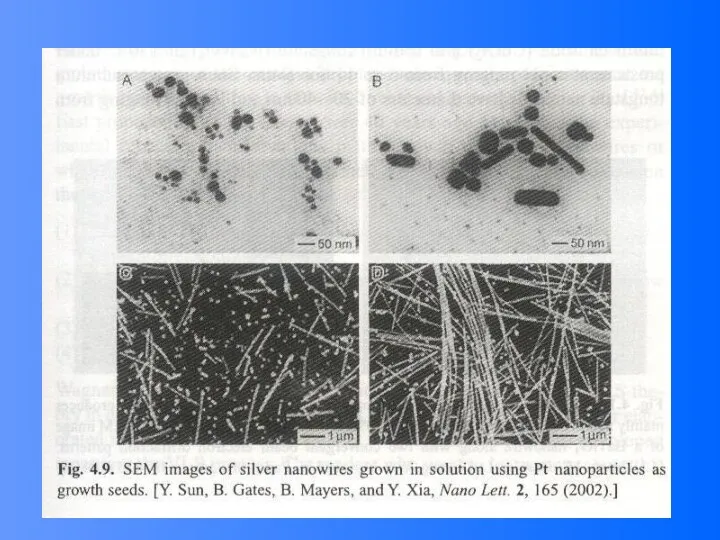
- 45. Growth of Ag Nanowire Using Pt Nanoparticles as Growth Seeds Precursor: AgNO3 Reduction agent: ethylene glycol
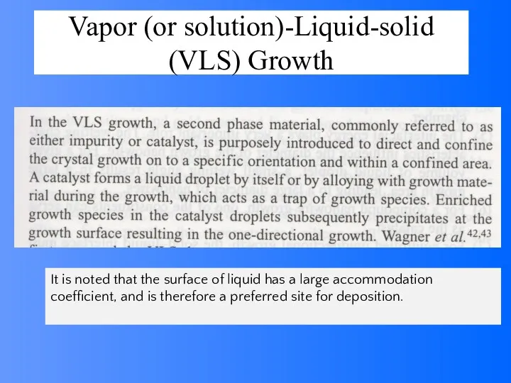
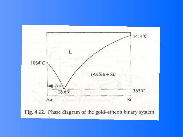
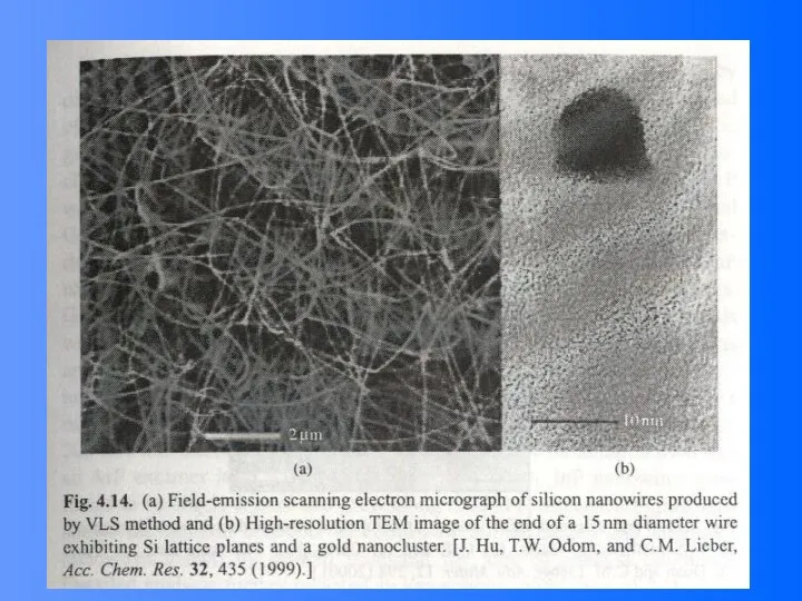
- 48. Vapor (or solution)-Liquid-solid (VLS) Growth It is noted that the surface of liquid has a large
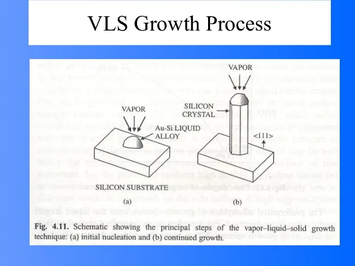
- 49. VLS Growth Process
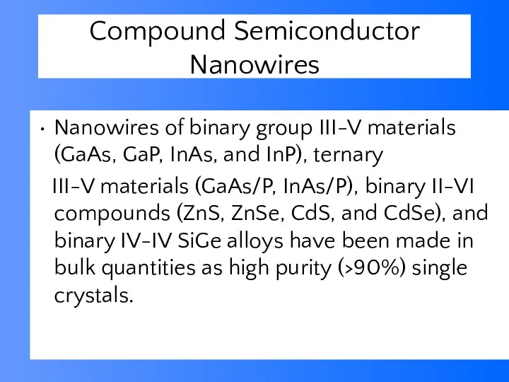
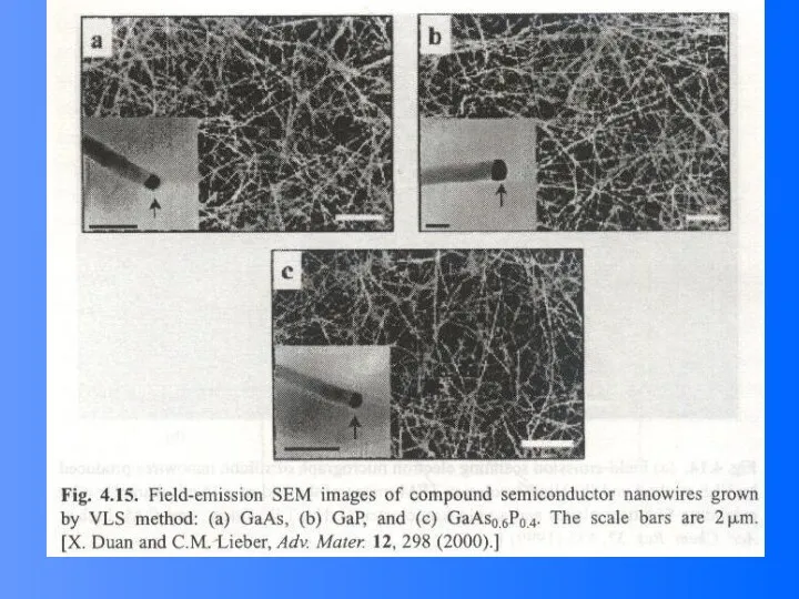
- 52. Compound Semiconductor Nanowires Nanowires of binary group III-V materials (GaAs, GaP, InAs, and InP), ternary III-V
- 54. Table 1. Summary of single crystal nanowires synthesized. The growth temperatures correspond to ranges explored in
- 59. Methods for Growth of CNTs Formation of nanotubes Note: The target may be made by pressing
- 60. CVD Growth of graphene Hydrocarbon gas flow Carbon dissolving Metal Copper has zero solubility of carbon
- 61. Template assisted nanowire growth Create a template for nanowires to grow within Based on aluminum’s unique
- 62. Anodization of aluminum Start with uniform layer of ~1mm Al Al serves as the anode, Pt
- 63. (T. Sands/ HEMI group http://www.mse.berkeley.edu/groups/Sands/HEMI/nanoTE.html) The alumina (Al2O3) template 100nm Si substrate alumina template (M. Sander)
- 64. Works well with thermoelectric materials and metals Process allows to remove/dissolve oxide barrier layer so that
- 66. Скачать презентацию
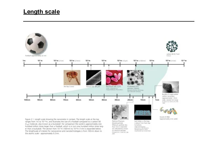
Length scale
Length scale
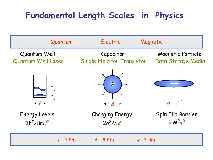
Fundamental Length Scales in Physics
Quantum Electric Magnetic
Quantum Well:
Quantum Well Laser
Capacitor:
Single Electron
Fundamental Length Scales in Physics
Quantum Electric Magnetic
Quantum Well:
Quantum Well Laser
Capacitor: Single Electron
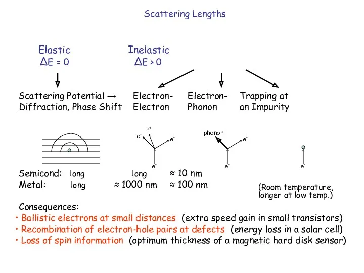
Elastic Inelastic
ΔE = 0 ΔE > 0
Scattering Potential → Electron- Electron-
ΔE = 0 ΔE > 0
Scattering Potential → Electron- Electron-
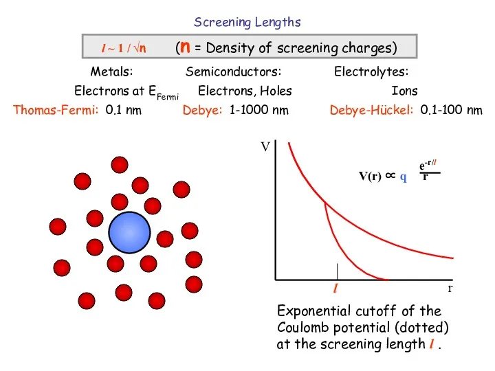
Screening Lengths
l ~ 1 / √n (n = Density of
Screening Lengths l ~ 1 / √n (n = Density of
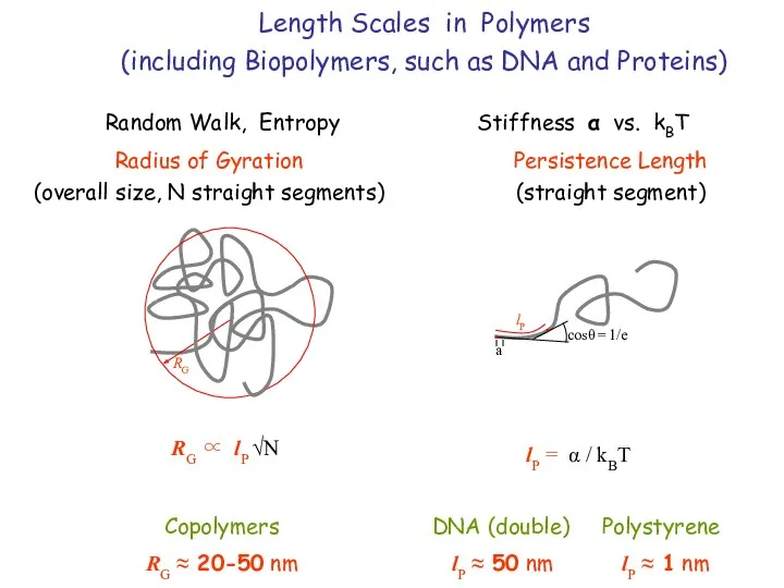
Length Scales in Polymers
(including Biopolymers, such as DNA and Proteins)
Random
Length Scales in Polymers
(including Biopolymers, such as DNA and Proteins)
Random
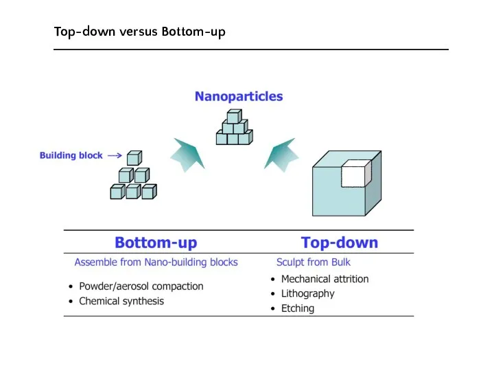
Top-down versus Bottom-up
Top-down versus Bottom-up
Nucleation and Growth of
Crystals
Nucleation and Growth of
Crystals
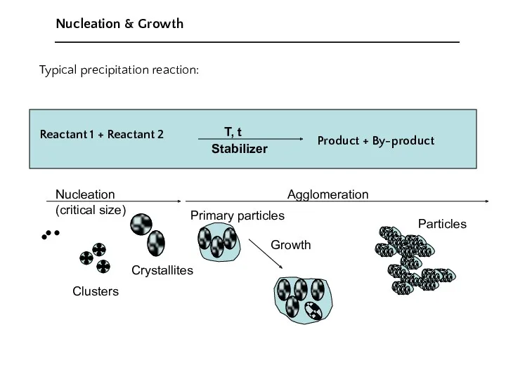
Typical precipitation reaction:
Reactant 1 + Reactant 2
Product + By-product
Nucleation & Growth
Typical precipitation reaction:
Reactant 1 + Reactant 2
Product + By-product
Nucleation & Growth
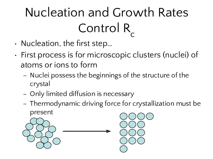
Nucleation and Growth Rates Control Rc
Nucleation, the first step…
First process is
Nucleation and Growth Rates Control Rc
Nucleation, the first step…
First process is
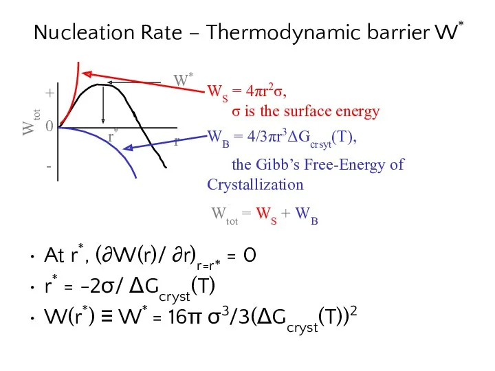
Nucleation Rate – Thermodynamic barrier W*
At r*, (∂W(r)/ ∂r)r=r* = 0
r*
Nucleation Rate – Thermodynamic barrier W*
At r*, (∂W(r)/ ∂r)r=r* = 0
r*
Bottom-up Approaches
Two approaches
thermodynamic equilibrium approach
generation of supersaturation
nucleation
subsequent growth
kinetic approach
limiting the amount
Bottom-up Approaches
Two approaches
thermodynamic equilibrium approach
generation of supersaturation
nucleation
subsequent growth
kinetic approach
limiting the amount
Homogeneous nucleation
Liquid, vapor or solid
supersaturation
temperature reduction
metal quantum dots in glass matrix
Homogeneous nucleation
Liquid, vapor or solid
supersaturation
temperature reduction
metal quantum dots in glass matrix
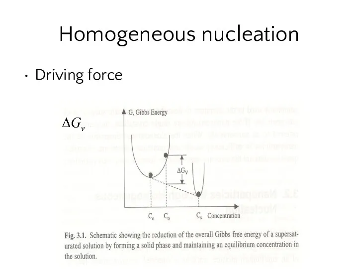
Homogeneous nucleation
Driving force
Fig 3.1
Homogeneous nucleation
Driving force
Fig 3.1
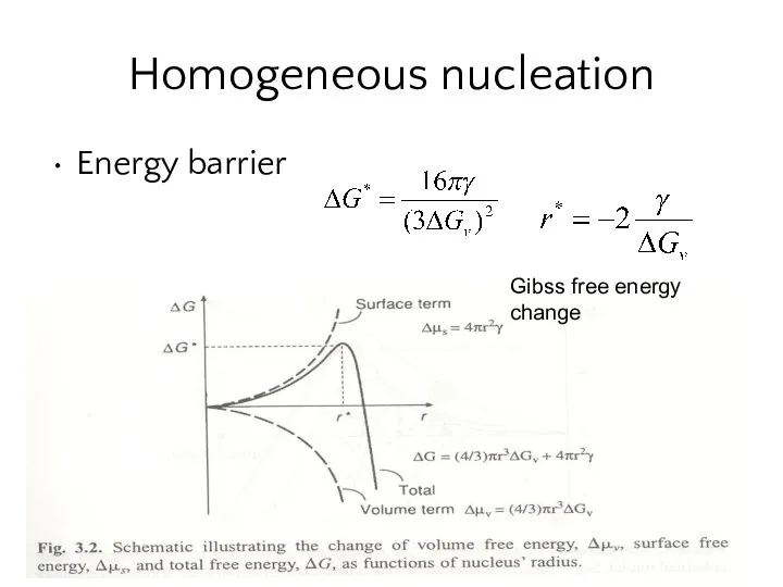
Homogeneous nucleation
Energy barrier
Gibss free energy change
Homogeneous nucleation
Energy barrier
Gibss free energy change
Nuclei
formation favor:
high initial concentration or supersaturation
low viscosity
low critical energy barrier
uniform nanoparticle
Nuclei
formation favor:
high initial concentration or supersaturation
low viscosity
low critical energy barrier
uniform nanoparticle
Nuclei growth
Steps
growth species generation
diffusion from bulk to the growth surface
adsorption
surface growth
size
Nuclei growth
Steps
growth species generation
diffusion from bulk to the growth surface
adsorption
surface growth
size
Ostwald ripening
Many small crystals form in a system initially but slowly
Ostwald ripening
Many small crystals form in a system initially but slowly
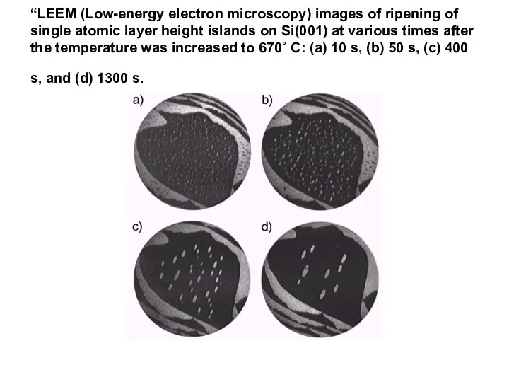
“LEEM (Low-energy electron microscopy) images of ripening of single atomic layer
“LEEM (Low-energy electron microscopy) images of ripening of single atomic layer
Metallic nanoparticles
Reduction of metal complexes in dilute solution
Diffusion-limited process maintaining
Example: nano-gold
Metallic nanoparticles
Reduction of metal complexes in dilute solution
Diffusion-limited process maintaining
Example: nano-gold
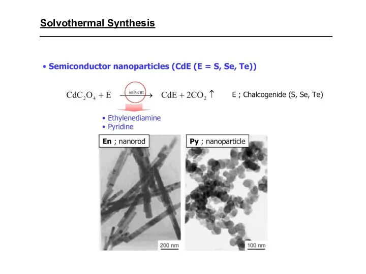
Semiconductor nanoparticles
Pyrolysis of organometallic precursor(s) dissolved in anhydrate solvents at elevated
Semiconductor nanoparticles
Pyrolysis of organometallic precursor(s) dissolved in anhydrate solvents at elevated
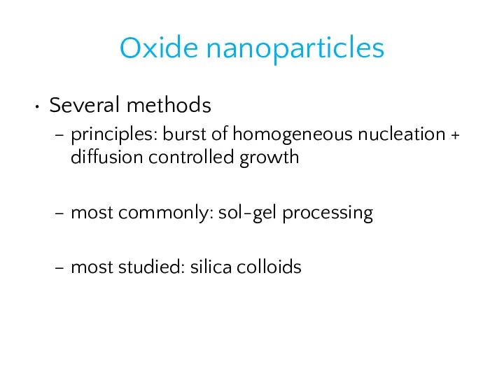
Oxide nanoparticles
Several methods
principles: burst of homogeneous nucleation + diffusion controlled growth
most
Oxide nanoparticles
Several methods
principles: burst of homogeneous nucleation + diffusion controlled growth
most
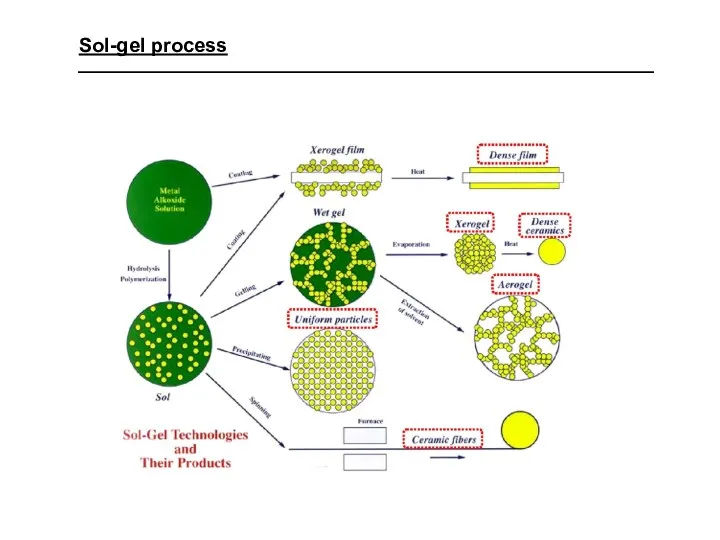
Sol-gel process
Sol-gel process
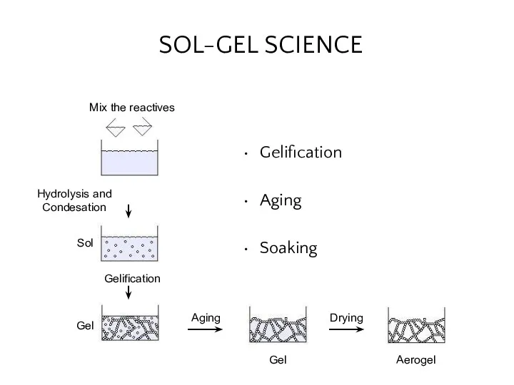
SOL-GEL SCIENCE
Gelification
Aging
Soaking
Mix the reactives
Sol
Gel
Gel
Aerogel
Hydrolysis and Condesation
Gelification
Aging
Drying
SOL-GEL SCIENCE
Gelification
Aging
Soaking
Mix the reactives
Sol
Gel
Gel
Aerogel
Hydrolysis and Condesation
Gelification
Aging
Drying
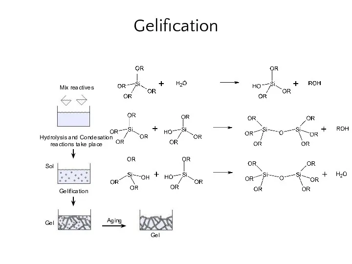
Gelification
Mix reactives
Sol
Gel
Gel
Gelification
Aging
Hydrolysis and Condesation reactions take place
Gelification
Mix reactives
Sol
Gel
Gel
Gelification
Aging
Hydrolysis and Condesation reactions take place
Sol-gel process
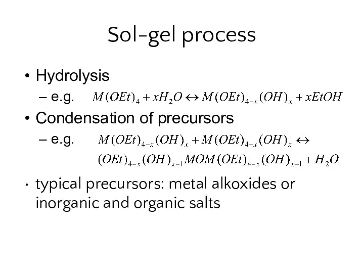
Hydrolysis
e.g.
Condensation of precursors
e.g.
typical precursors: metal alkoxides or inorganic and
Sol-gel process
Hydrolysis
e.g.
Condensation of precursors
e.g.
typical precursors: metal alkoxides or inorganic and
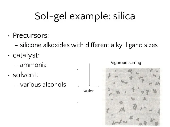
Sol-gel example: silica
Precursors:
silicone alkoxides with different alkyl ligand sizes
catalyst:
ammonia
solvent:
various alcohols
water
Vigorous stirring
Sol-gel example: silica
Precursors:
silicone alkoxides with different alkyl ligand sizes
catalyst:
ammonia
solvent:
various alcohols
water
Vigorous stirring
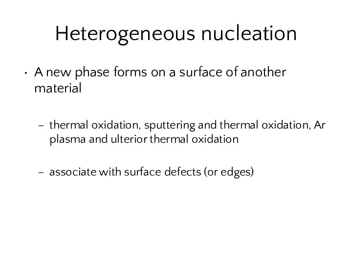
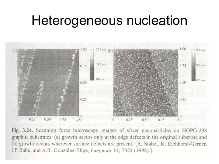
Heterogeneous nucleation
A new phase forms on a surface of another material
thermal
Heterogeneous nucleation
A new phase forms on a surface of another material
thermal
Heterogeneous nucleation
Heterogeneous nucleation
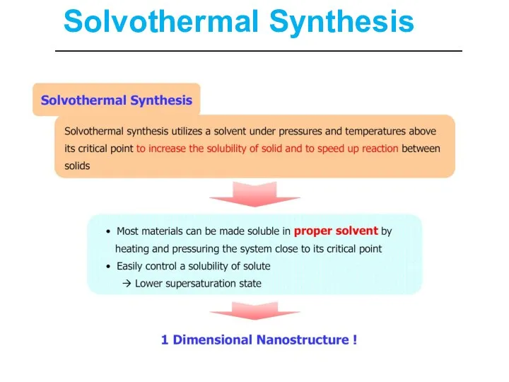
Solvothermal Synthesis
Solvothermal Synthesis
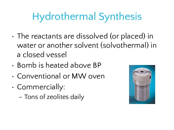
Hydrothermal Synthesis
The reactants are dissolved (or placed) in water or another
Hydrothermal Synthesis
The reactants are dissolved (or placed) in water or another
Solvothermal Synthesis
Solvothermal Synthesis
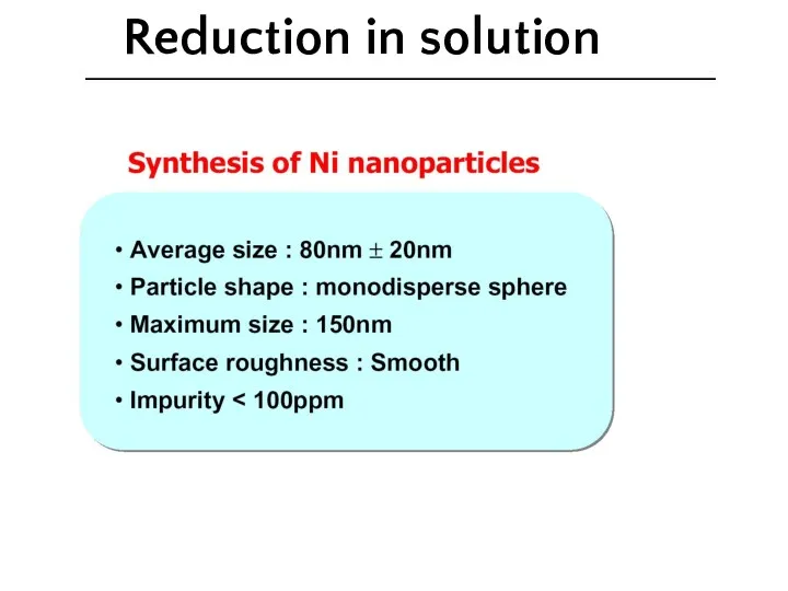
Reduction in solution
Reduction in solution
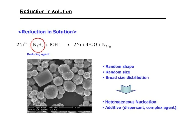
Reduction in solution
Reduction in solution
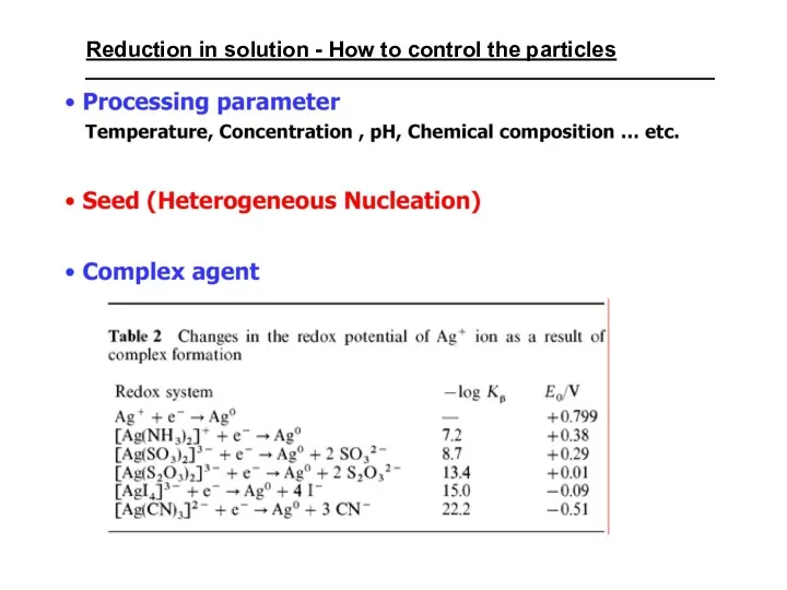
Reduction in solution - How to control the particles
Reduction in solution - How to control the particles
Reduction in solution - How to control the particles
Seed-mediated growth
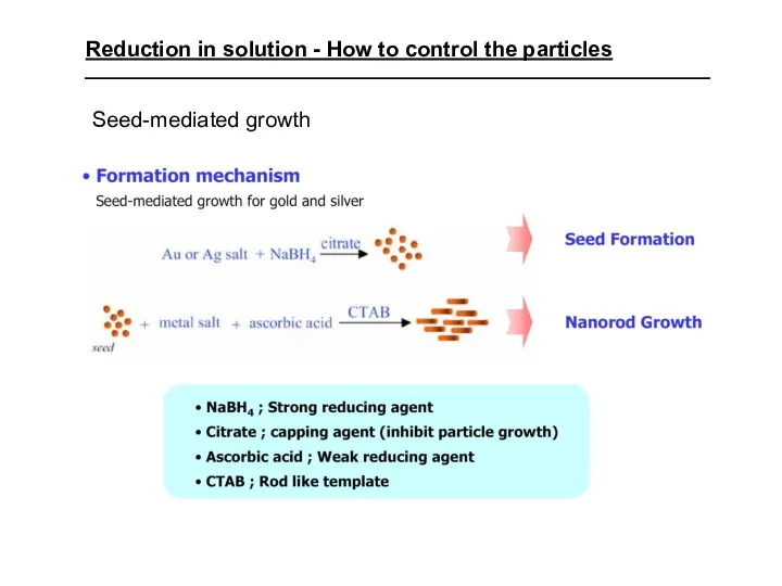
Reduction in solution - How to control the particles
Seed-mediated growth
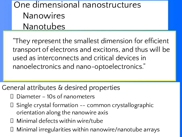
One dimensional nanostructures
Nanowires
Nanotubes
“They represent the smallest dimension for efficient transport of
One dimensional nanostructures
Nanowires
Nanotubes
“They represent the smallest dimension for efficient transport of
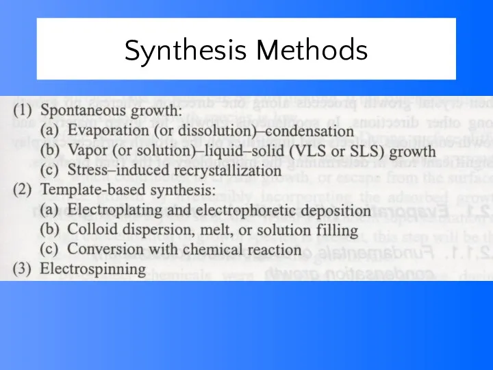
Synthesis Methods
Synthesis Methods
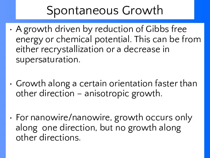
Spontaneous Growth
A growth driven by reduction of Gibbs free energy or
Spontaneous Growth
A growth driven by reduction of Gibbs free energy or
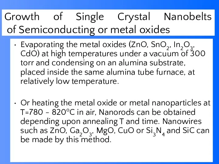
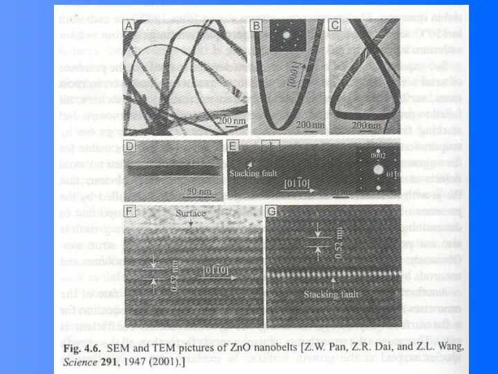
Growth of Single Crystal Nanobelts
of Semiconducting or metal oxides
Evaporating the
Growth of Single Crystal Nanobelts
of Semiconducting or metal oxides
Evaporating the
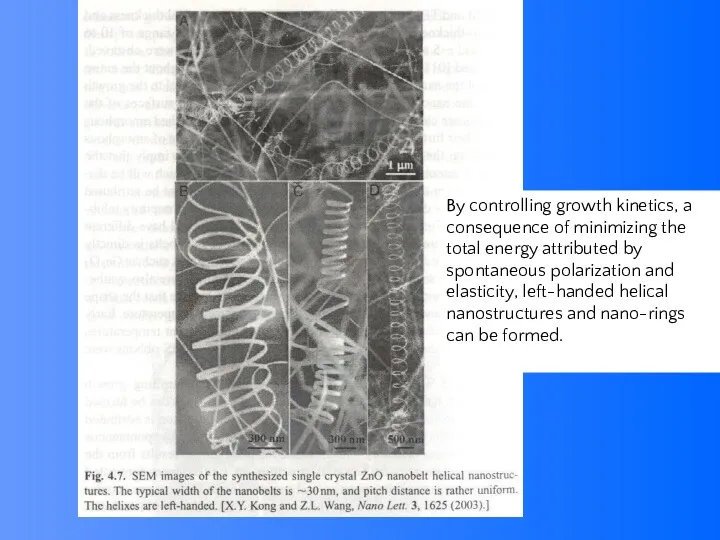
By controlling growth kinetics, a consequence of minimizing the total energy
By controlling growth kinetics, a consequence of minimizing the total energy
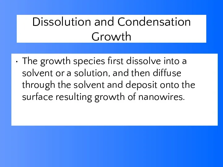
Dissolution and Condensation Growth
The growth species first dissolve into a solvent
Dissolution and Condensation Growth
The growth species first dissolve into a solvent
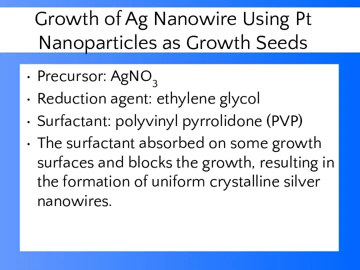
Growth of Ag Nanowire Using Pt Nanoparticles as Growth Seeds
Precursor: AgNO3
Reduction
Growth of Ag Nanowire Using Pt Nanoparticles as Growth Seeds
Precursor: AgNO3
Reduction
Vapor (or solution)-Liquid-solid (VLS) Growth
It is noted that the surface of
Vapor (or solution)-Liquid-solid (VLS) Growth
It is noted that the surface of
VLS Growth Process
VLS Growth Process
Compound Semiconductor Nanowires
Nanowires of binary group III-V materials (GaAs, GaP, InAs,
Compound Semiconductor Nanowires
Nanowires of binary group III-V materials (GaAs, GaP, InAs,
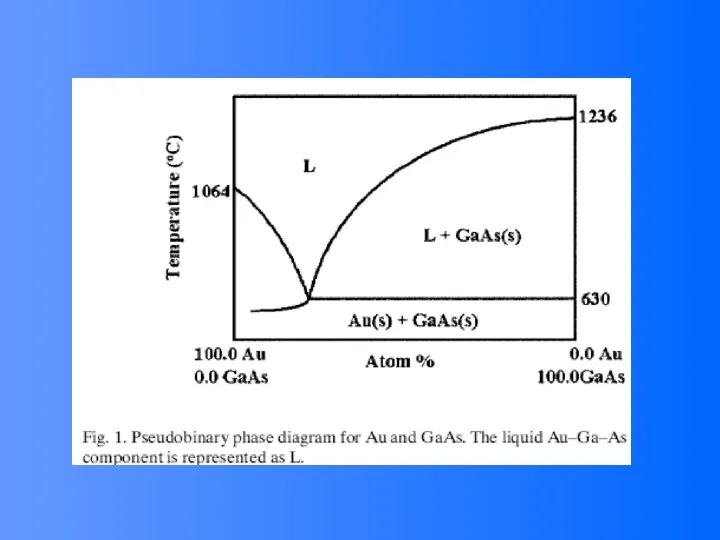
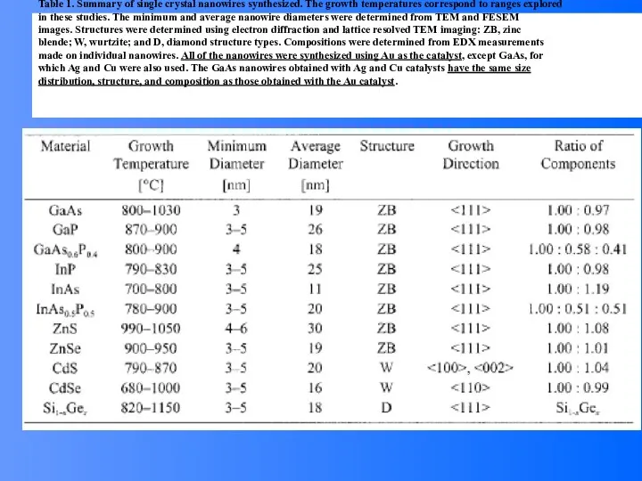
Table 1. Summary of single crystal nanowires synthesized. The growth temperatures
Table 1. Summary of single crystal nanowires synthesized. The growth temperatures
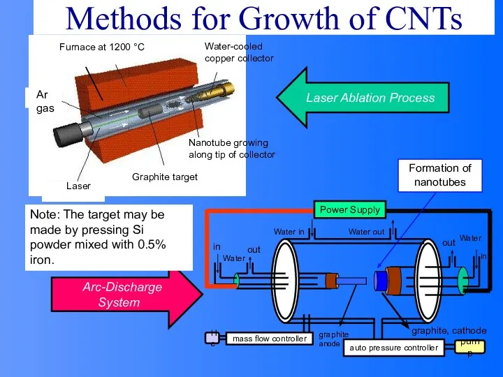
Methods for Growth of CNTs
Formation of nanotubes
Note: The target may be
Methods for Growth of CNTs
Formation of nanotubes
Note: The target may be
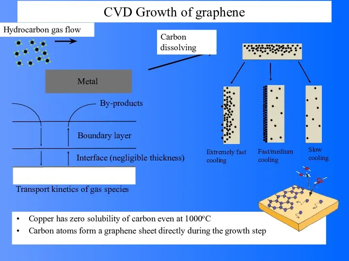
CVD Growth of graphene
Hydrocarbon gas flow
Carbon dissolving
Metal
Copper has zero solubility of
CVD Growth of graphene
Hydrocarbon gas flow
Carbon dissolving
Metal
Copper has zero solubility of
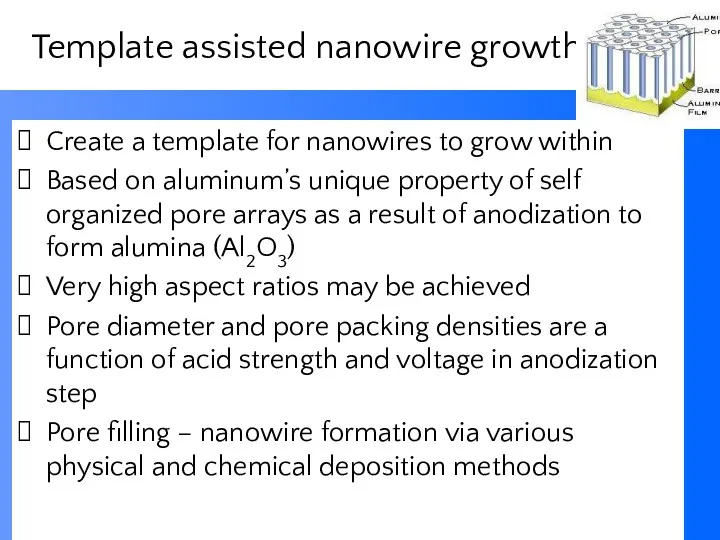
Template assisted nanowire growth
Create a template for nanowires to grow within
Based
Template assisted nanowire growth
Create a template for nanowires to grow within
Based
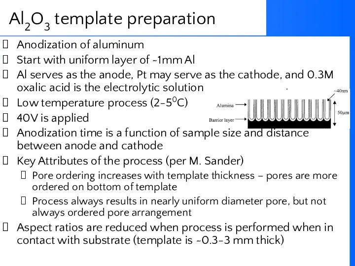
Anodization of aluminum
Start with uniform layer of ~1mm Al
Al serves as
Anodization of aluminum
Start with uniform layer of ~1mm Al
Al serves as
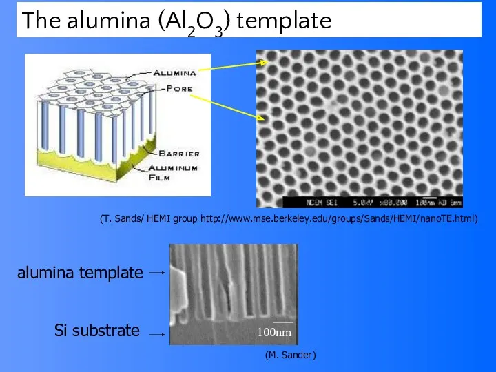
(T. Sands/ HEMI group http://www.mse.berkeley.edu/groups/Sands/HEMI/nanoTE.html)
The alumina (Al2O3) template
100nm
Si substrate
alumina template
(M. Sander)
(T. Sands/ HEMI group http://www.mse.berkeley.edu/groups/Sands/HEMI/nanoTE.html)
The alumina (Al2O3) template
100nm
Si substrate
alumina template
(M. Sander)
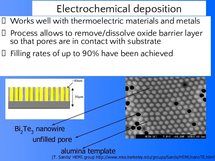
Works well with thermoelectric materials and metals
Process allows to remove/dissolve
Works well with thermoelectric materials and metals
Process allows to remove/dissolve
 Welcome to our Christmas (quiz)
 Modal verbs in school life
 How to fix grammar mistakes
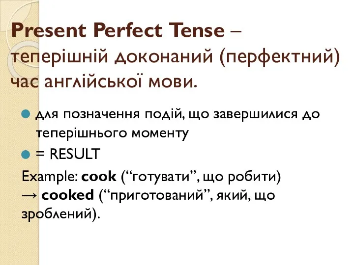 Present Perfect Tense
 Как написать письмо? Почтовая открытка: задание
 Система вправ для навчання іноземноі мови
 The competition for English language Learn to win. MY IDOL
 Guess these colour idioms 2
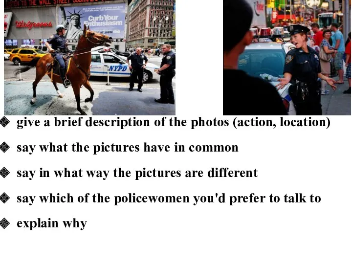 Сравнение полицейских
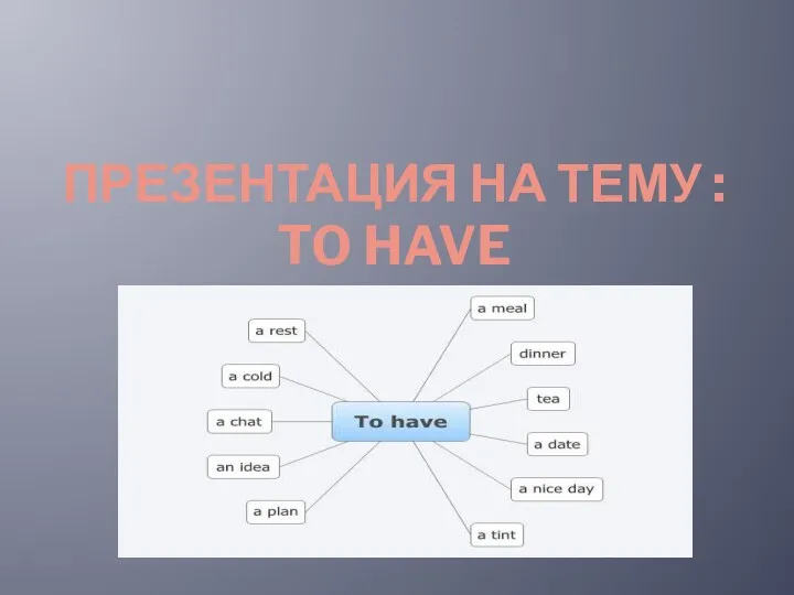 Глагол TO HAVE
 Welcome to Great Britain
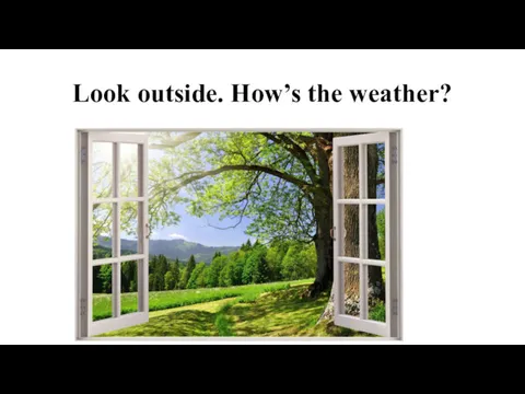 Look outside. How’s the weather?
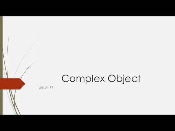 Сложное дополнение
 Famous people of Great Britain
 Environmental Protection ( Охрана окружающей среды). 7 класс
 Marking Punctuation
 My favorite holiday
 Plan for today
 How to shop propertly
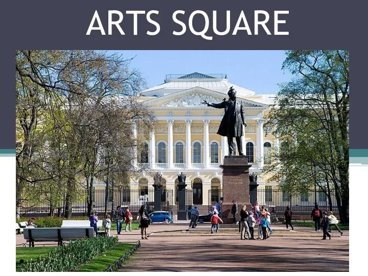 St. Petersburg architecture
 Content and language integrated learning
 Повторение по английскому языку
 Согласование времен в английском языке
 Условные предложения. Conditionals
 He loves jelly (lesson 20)
 Food. Еда
 Irregular plurals
 Chestnut