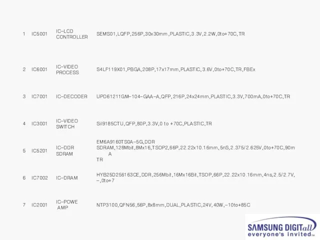
- Carnelian Р416

Содержание
- 2. 1. Introduction to PDP 2. Manufacturing & Structure of Panel 3. PDP Driving Characteristics 4. CARNELIAN
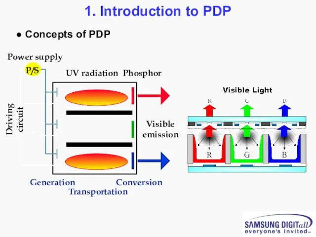
- 3. 1. Introduction to PDP ● Concepts of PDP
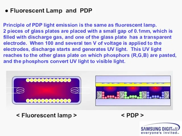
- 4. Principle of PDP light emission is the same as fluorescent lamp. 2 pieces of glass plates
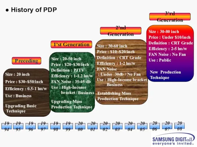
- 5. ● History of PDP Size : 20 inch Price : $30~$50/inch Efficiency : 0.5-1 lm/w Use
- 6. - Thin Type TV - Large Scale : 80” possible - Light Weight (42” Scale) :
- 7. Manufacturing & Structure of Panel
- 8. 2. Manufacturing & Structure of Panel ● Cell Structure of Panel
- 9. ● Cell Structure of Panel
- 10. ● Electro Arrangement of PDP(SDI Panel - SD)
- 11. Driving Circuit - Discharge Switching MgO Thin Film - 2’nd Electron Radiation - Forming wall charge
- 12. ● Process of Panel Manufacturing
- 13. ● Process of Panel Manufacturing
- 14. PDP Driving Characteristics
- 15. ■.SMPS(Switching Mode Power Supply) : It is the supplier to provide voltage and current to work
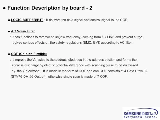
- 16. ■.LOGIC BUFFER(E,F) : It delivers the data signal and control signal to the COF. ■.AC Noise
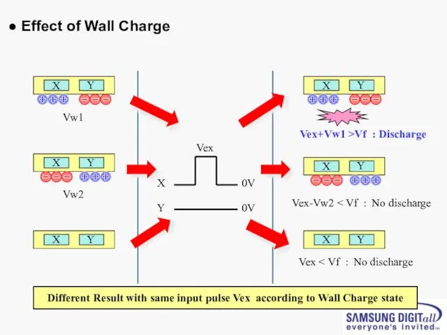
- 17. X Y X Y X Y 0V 0V Vex Vw1 Vw2 X Y Vex+Vw1 >Vf :
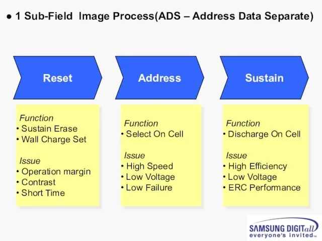
- 18. Reset Address Sustain Function Sustain Erase Wall Charge Set Issue Operation margin Contrast Short Time Function
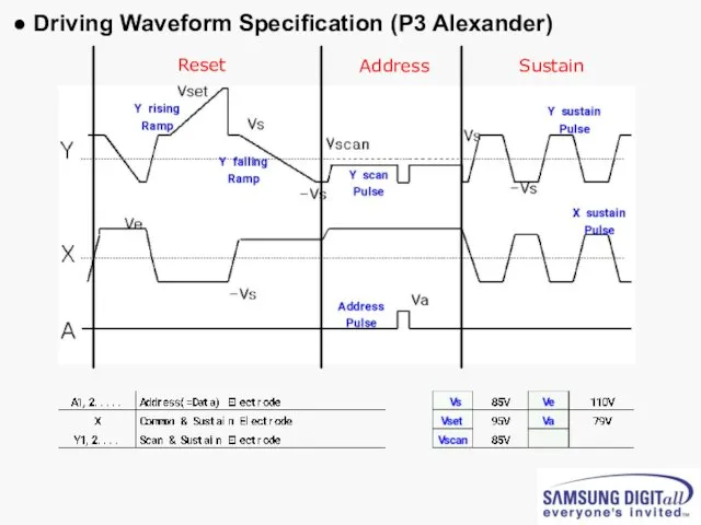
- 19. ● Driving Waveform Specification (P3 Alexander) Reset Address Sustain
- 20. ● Address Operation
- 21. Display cells through strong Sustain discharge. ● Sustain Operation
- 22. RED 4096 Levels 68.7 Billion Colors 1 - Pixel Level of Luminance ● Combination of R,G,B
- 23. Number of Pulses Lights 1 2 4 2048 1 2 4 2048 ● Luminance Control
- 24. ● 1 Picture Structure by 12 Sub-Field - 1
- 25. ● 1 Picture Structure by 12 Sub-Field - 2
- 26. ● 1 Picture Structure by 12 Sub-Field - 3
- 27. ● 1 Picture Structure by 12 Sub-Field - 4
- 28. ● 1 Picture Structure by 12 Sub-Field - 5
- 29. ● 1 Picture Structure by 12 Sub-Field - ……
- 30. ● 1 Picture Structure by 12 Sub-Field - 11
- 31. ● 1 Picture Structure by 12 Sub-Field - 12
- 32. 3. CARNELIAN Training
- 33. ● Comparison with other Models
- 34. ● Picture of PS50A416P1DX Set [Back view]
- 35. ● Picture of CARNELIAN 50” W3 PDP Module [Back view]
- 36. ● General PDP SET Block Diagram
- 37. Carnelian Block Diagram (PS50A416P1DX) Audio AMP NTP3100 DDR 8M*16 LVDS Input Jack Display Panel Scaler (256-QFP)
- 38. ● Picture of PS50A416P1DX Chassis - Top 1.Scaler 2.FBE3 6.DRAM 5.DDR 3.DTV Micom 4.HDMI switch 7.Sound
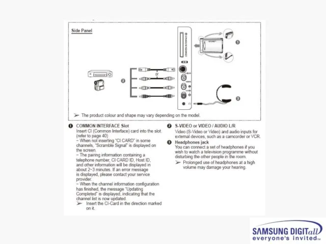
- 40. ● Picture of PS50A416P1DX Chassis - Bottom DTV flash ATV flash Comp/iDTV switch
- 41. ● PS50A416P1DX SW update method (ATV software) D-SUB Cable 1. Connect the PC and PDP using
- 42. 3. Click “Connect” button 4. Now the connection with the SET is established. Click the “확인”
- 43. 5. Connect the Power cord and click “Read” 6. Click the new “Read” button
- 44. 7. Select the upgrade file
- 45. 8. Click “Auto” button, uncheck the Blank and Verify options and click “Run”
- 46. 9. The download progress bar appears and D/L information is shown in the info window
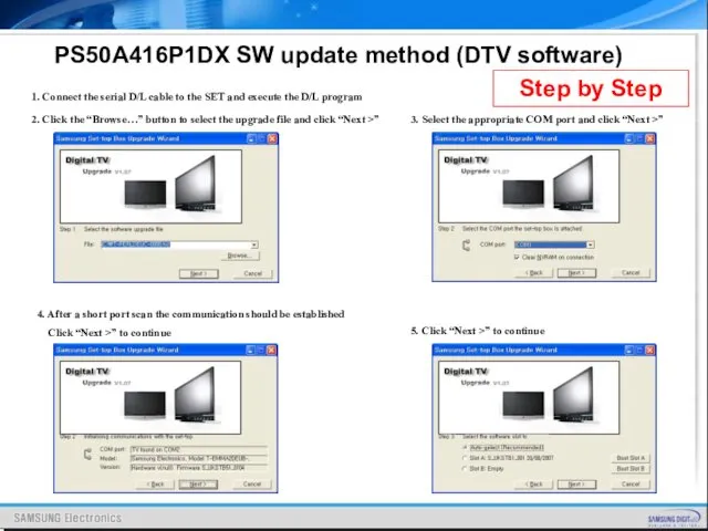
- 47. PS50A416P1DX SW update method (DTV software) 1. Connect the serial D/L cable to the SET and
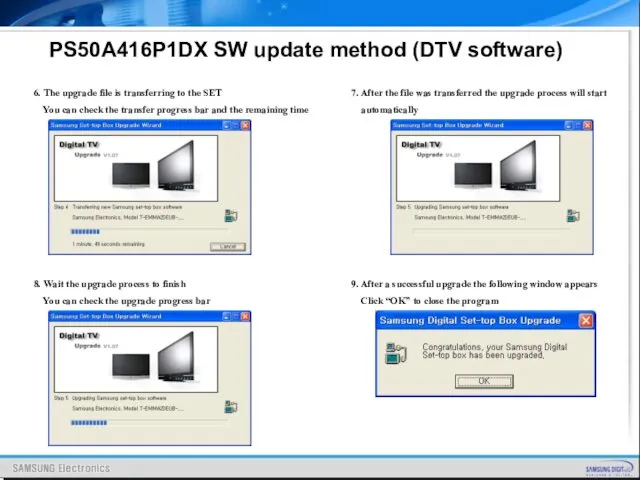
- 48. PS50A416P1DX SW update method (DTV software) 6. The upgrade file is transferring to the SET You
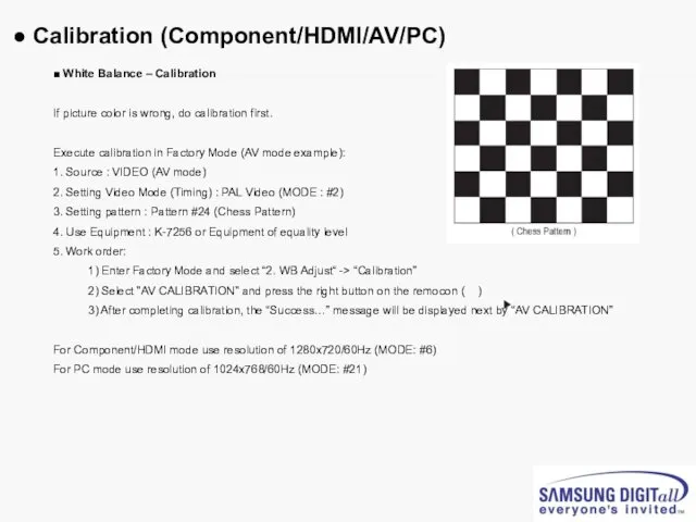
- 49. ● Calibration (Component/HDMI/AV/PC) ■ White Balance – Calibration If picture color is wrong, do calibration first.
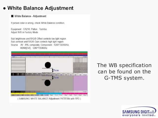
- 50. ● White Balance Adjustment The WB specification can be found on the G-TMS system.
- 51. ● Picture condition in Factory mode / during WB adjust ● Factory mode OSD
- 56. Accessories
- 57. 5. Trouble shooting
- 58. ● Check List in advance ■. Each cable connection condition check - Cable is connected correctly
- 59. ● No Power - Not operate front LED Not operate SMPS relay ① ① ② 1
- 60. ● SMPS relay on off continually Operate Protection circuit because of some Ass’y problem CN810 CN809
- 61. ● No display but sound is normal X or Y or Logic or Y Buffer board
- 62. ● No sound but display is normal Speaker wire is not connect Video main board sound
- 63. ● PDP Dot Module SPEC – SDI module ※ Special Management Items 1) It is Cell-Defect
- 64. ● A-Zone / B–Zone Size
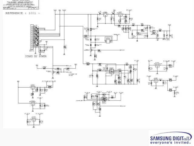
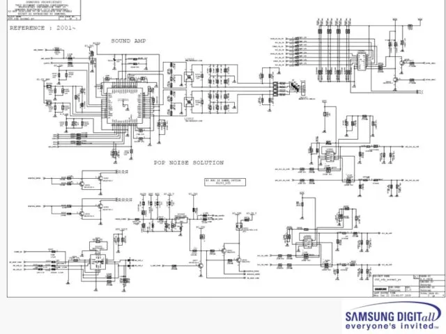
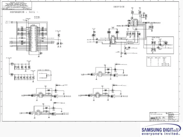
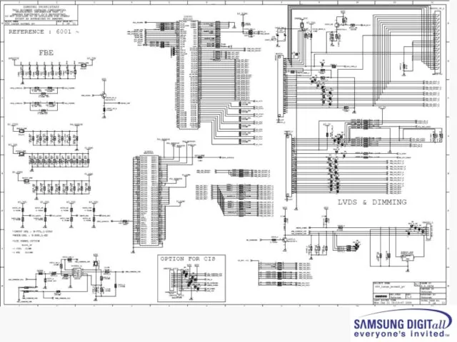
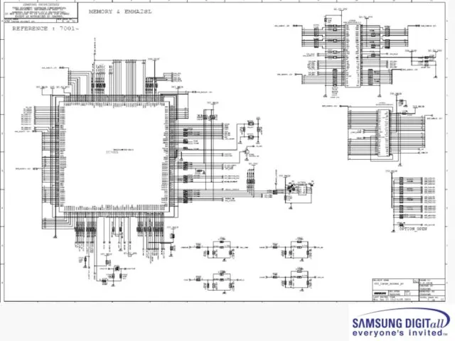
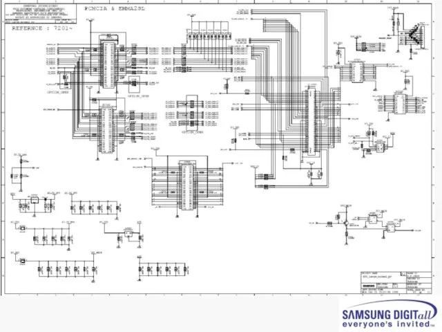
- 65. 6.CIRCUIT DIAGRAM
- 77. Скачать презентацию
1. Introduction to PDP
2. Manufacturing & Structure of Panel
3. PDP Driving
2. Manufacturing & Structure of Panel
3. PDP Driving
1. Introduction to PDP
● Concepts of PDP
1. Introduction to PDP
● Concepts of PDP
Principle of PDP light emission is the same as fluorescent lamp.
Principle of PDP light emission is the same as fluorescent lamp.
● History of PDP
Size : 20 inch
Price : $30~$50/inch
Efficiency : 0.5-1
● History of PDP
Size : 20 inch
Price : $30~$50/inch
Efficiency : 0.5-1
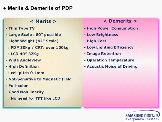
< Merits >
- Thin Type TV
- Large Scale : 80” possible
-
< Merits >
- Thin Type TV
- Large Scale : 80” possible
-

Manufacturing &
Structure of Panel
Manufacturing &
Structure of Panel
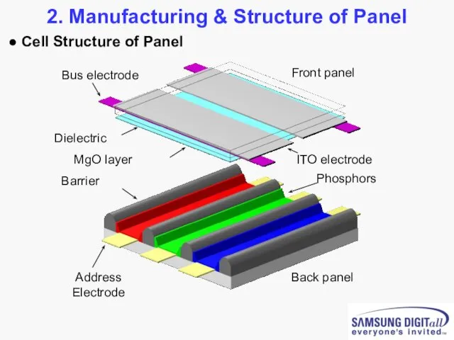
2. Manufacturing & Structure of Panel
● Cell Structure of Panel
2. Manufacturing & Structure of Panel
● Cell Structure of Panel
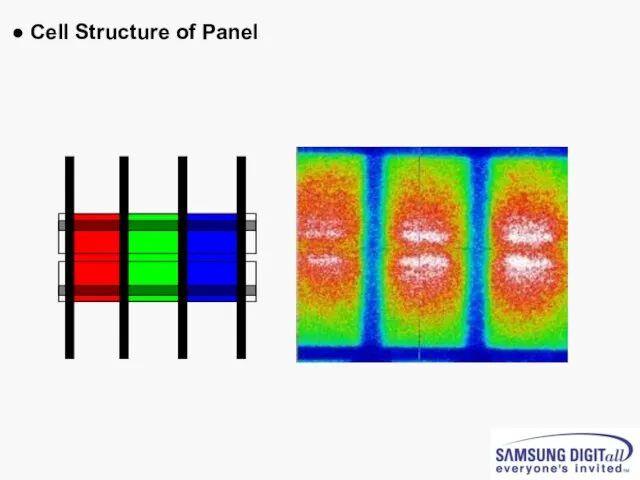
● Cell Structure of Panel
● Cell Structure of Panel
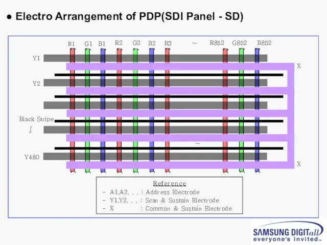
● Electro Arrangement of PDP(SDI Panel - SD)
● Electro Arrangement of PDP(SDI Panel - SD)
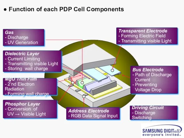
Driving Circuit
- Discharge Switching
MgO Thin Film
- 2’nd Electron Radiation
- Forming wall
Driving Circuit
- Discharge Switching
MgO Thin Film
- 2’nd Electron Radiation
- Forming wall
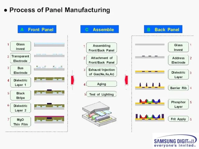
● Process of Panel Manufacturing
● Process of Panel Manufacturing
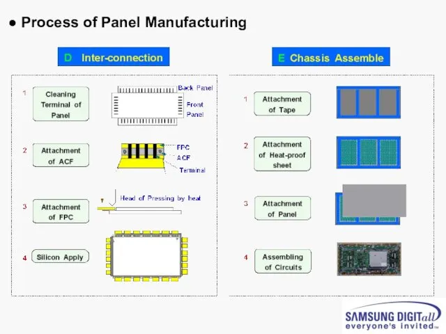
● Process of Panel Manufacturing
● Process of Panel Manufacturing

PDP Driving
Characteristics
PDP Driving
Characteristics
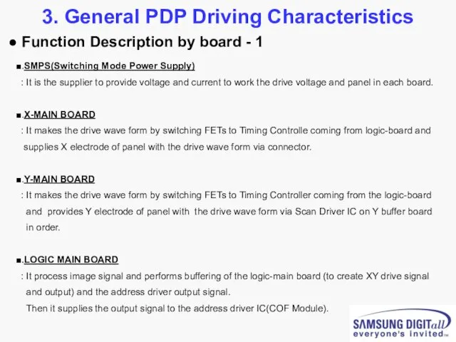
■.SMPS(Switching Mode Power Supply)
: It is the supplier to provide
■.SMPS(Switching Mode Power Supply)
: It is the supplier to provide
■.LOGIC BUFFER(E,F) : It delivers the data signal and control signal
■.LOGIC BUFFER(E,F) : It delivers the data signal and control signal
X
Y
X
Y
X
Y
0V
0V
Vex
Vw1
Vw2
X
Y
Vex+Vw1 >Vf : Discharge
X
Y
Vex-Vw2 < Vf : No discharge
X
Y
X
Y
Vex < Vf
X
Y
X
Y
X
Y
0V
0V
Vex
Vw1
Vw2
X
Y
Vex+Vw1 >Vf : Discharge
X
Y
Vex-Vw2 < Vf : No discharge
X
Y
X
Y
Vex < Vf
Reset
Address
Sustain
Function
Sustain Erase
Wall Charge Set
Issue
Operation margin
Contrast
Short Time
Function
Reset
Address
Sustain
Function
Sustain Erase
Wall Charge Set
Issue
Operation margin
Contrast
Short Time
Function
● Driving Waveform Specification (P3 Alexander)
Reset
Address
Sustain
● Driving Waveform Specification (P3 Alexander)
Reset
Address
Sustain
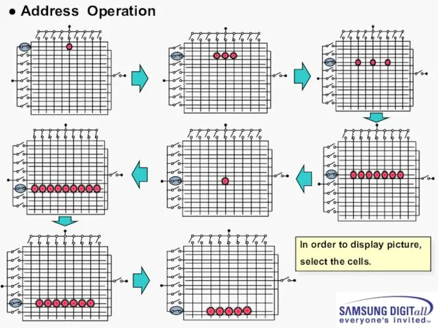
● Address Operation
● Address Operation
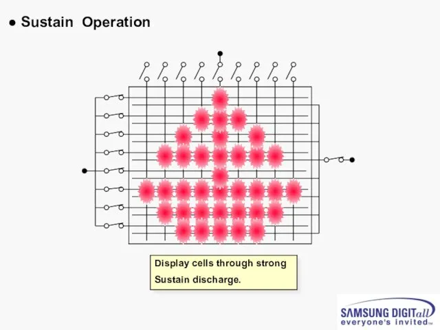
Display cells through strong
Sustain discharge.
● Sustain Operation
Display cells through strong
Sustain discharge.
● Sustain Operation
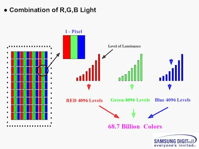
RED 4096 Levels
68.7 Billion Colors
1 - Pixel
Level of Luminance
● Combination of
RED 4096 Levels
68.7 Billion Colors
1 - Pixel
Level of Luminance
● Combination of
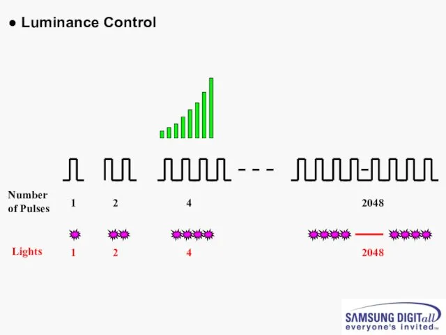
Number of Pulses
Lights
1
2
4
2048
1
2
4
2048
● Luminance Control
Number of Pulses
Lights
1
2
4
2048
1
2
4
2048
● Luminance Control
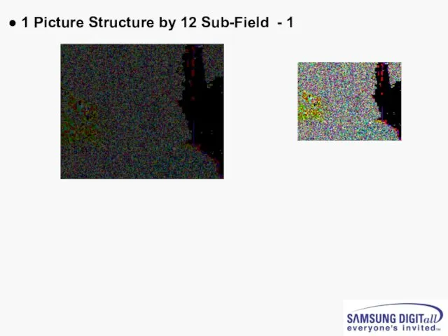
● 1 Picture Structure by 12 Sub-Field - 1
● 1 Picture Structure by 12 Sub-Field - 1
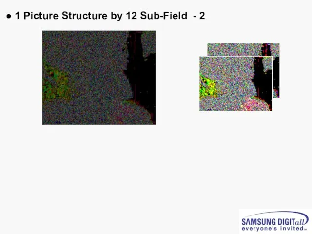
● 1 Picture Structure by 12 Sub-Field - 2
● 1 Picture Structure by 12 Sub-Field - 2
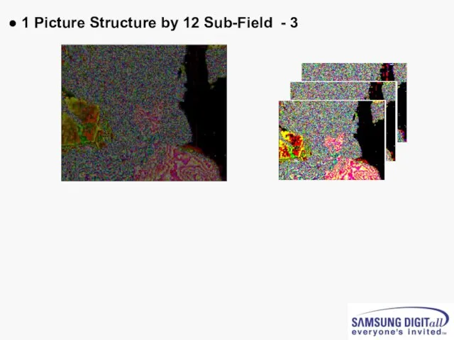
● 1 Picture Structure by 12 Sub-Field - 3
● 1 Picture Structure by 12 Sub-Field - 3
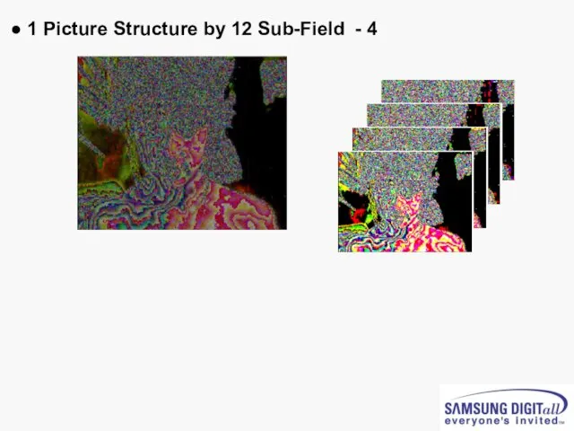
● 1 Picture Structure by 12 Sub-Field - 4
● 1 Picture Structure by 12 Sub-Field - 4
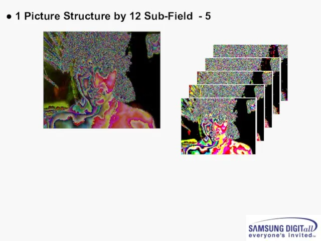
● 1 Picture Structure by 12 Sub-Field - 5
● 1 Picture Structure by 12 Sub-Field - 5
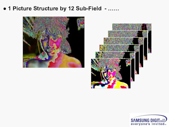
● 1 Picture Structure by 12 Sub-Field - ……
● 1 Picture Structure by 12 Sub-Field - ……
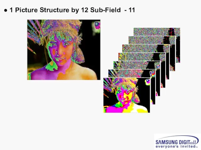
● 1 Picture Structure by 12 Sub-Field - 11
● 1 Picture Structure by 12 Sub-Field - 11
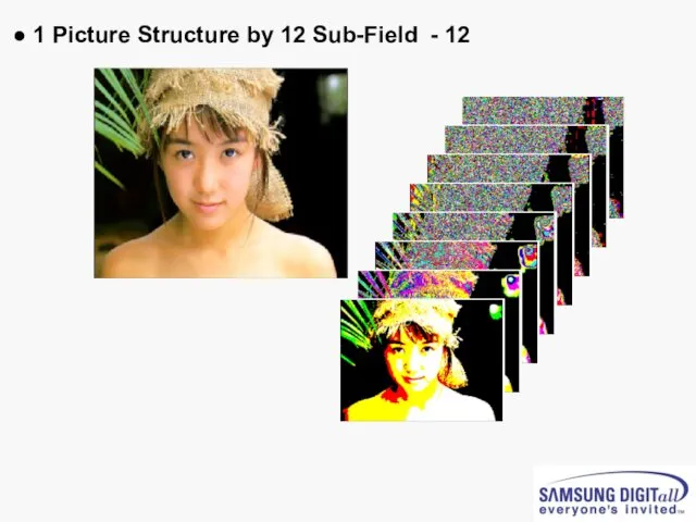
● 1 Picture Structure by 12 Sub-Field - 12
● 1 Picture Structure by 12 Sub-Field - 12

3. CARNELIAN Training
3. CARNELIAN Training
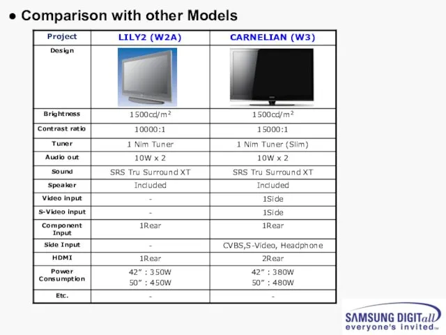
● Comparison with other Models
● Comparison with other Models
![● Picture of PS50A416P1DX Set [Back view]](/_ipx/f_webp&q_80&fit_contain&s_1440x1080/imagesDir/jpg/97107/slide-33.jpg)
● Picture of PS50A416P1DX Set [Back view]
● Picture of PS50A416P1DX Set [Back view]
![● Picture of CARNELIAN 50” W3 PDP Module [Back view]](/_ipx/f_webp&q_80&fit_contain&s_1440x1080/imagesDir/jpg/97107/slide-34.jpg)
● Picture of CARNELIAN 50” W3 PDP Module [Back view]
● Picture of CARNELIAN 50” W3 PDP Module [Back view]
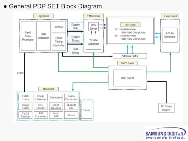
● General PDP SET Block Diagram
● General PDP SET Block Diagram
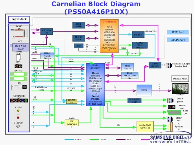
Carnelian Block Diagram (PS50A416P1DX)
Audio AMP
NTP3100
DDR
8M*16
LVDS
Input Jack
Display Panel
Scaler
(256-QFP)
Micom
3D Comb
Multi Decoder
De-interlacer
Scaler
LVDS Out
WXGA
Carnelian Block Diagram (PS50A416P1DX)
Audio AMP
NTP3100
DDR
8M*16
LVDS
Input Jack
Display Panel
Scaler
(256-QFP)
Micom
3D Comb
Multi Decoder
De-interlacer
Scaler
LVDS Out
WXGA
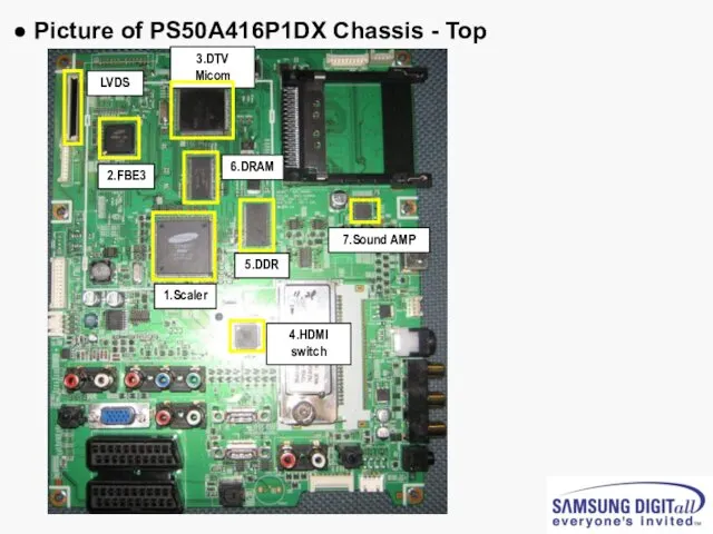
● Picture of PS50A416P1DX Chassis - Top
1.Scaler
2.FBE3
6.DRAM
5.DDR
3.DTV Micom
4.HDMI switch
7.Sound AMP
LVDS
● Picture of PS50A416P1DX Chassis - Top
1.Scaler
2.FBE3
6.DRAM
5.DDR
3.DTV Micom
4.HDMI switch
7.Sound AMP
LVDS
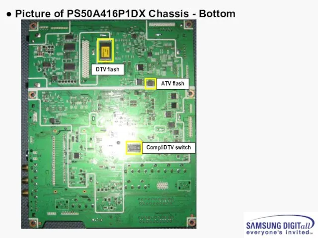
● Picture of PS50A416P1DX Chassis - Bottom
DTV flash
ATV flash
Comp/iDTV switch
● Picture of PS50A416P1DX Chassis - Bottom
DTV flash
ATV flash
Comp/iDTV switch
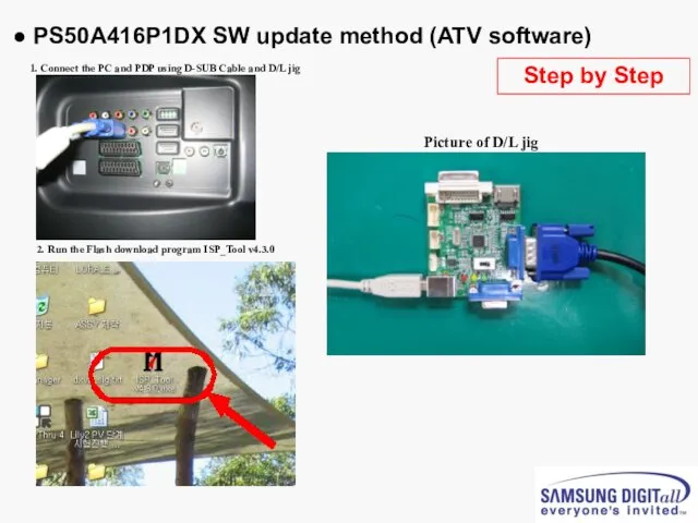
● PS50A416P1DX SW update method (ATV software)
D-SUB Cable
1. Connect the PC
● PS50A416P1DX SW update method (ATV software)
D-SUB Cable
1. Connect the PC
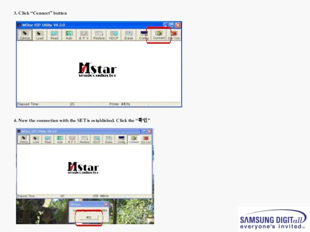
3. Click “Connect” button
4. Now the connection with the SET
3. Click “Connect” button
4. Now the connection with the SET
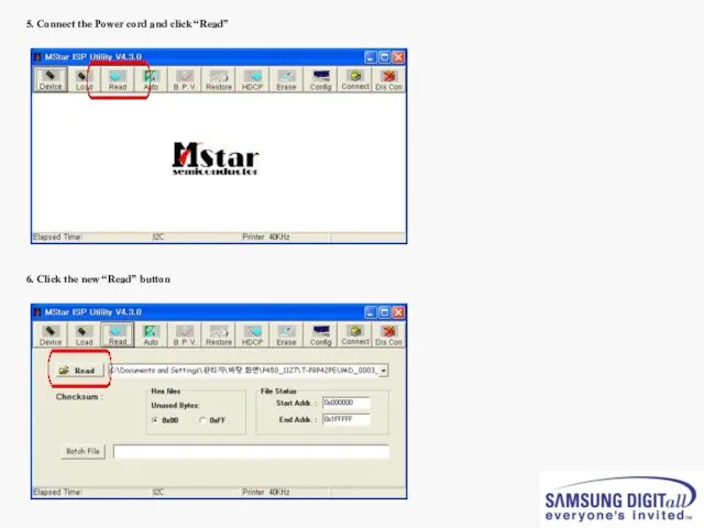
5. Connect the Power cord and click “Read”
6. Click the new
5. Connect the Power cord and click “Read”
6. Click the new
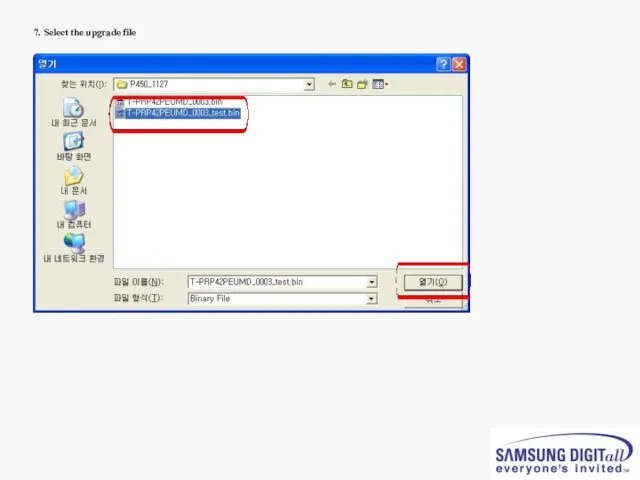
7. Select the upgrade file
7. Select the upgrade file
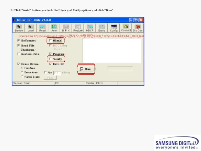
8. Click “Auto” button, uncheck the Blank and Verify options and
8. Click “Auto” button, uncheck the Blank and Verify options and
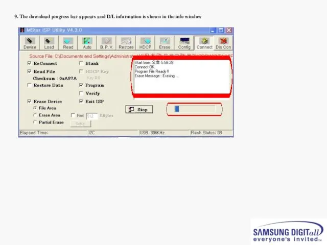
9. The download progress bar appears and D/L information is shown
9. The download progress bar appears and D/L information is shown
PS50A416P1DX SW update method (DTV software)
1. Connect the serial D/L cable
PS50A416P1DX SW update method (DTV software)
1. Connect the serial D/L cable
PS50A416P1DX SW update method (DTV software)
6. The upgrade file is transferring
PS50A416P1DX SW update method (DTV software)
6. The upgrade file is transferring
● Calibration (Component/HDMI/AV/PC)
■ White Balance – Calibration
If picture color is wrong,
● Calibration (Component/HDMI/AV/PC)
■ White Balance – Calibration
If picture color is wrong,
● White Balance Adjustment
The WB specification can be found on the
● White Balance Adjustment
The WB specification can be found on the
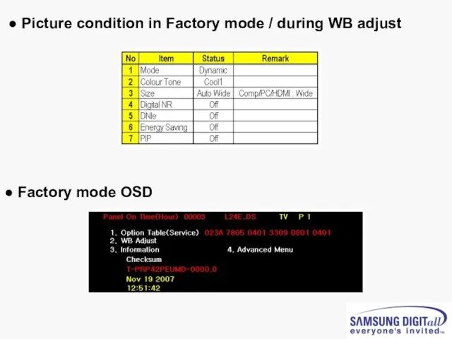
● Picture condition in Factory mode / during WB adjust
● Factory
● Picture condition in Factory mode / during WB adjust
● Factory
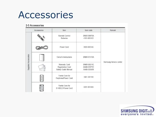
Accessories
Accessories

5. Trouble shooting
5. Trouble shooting
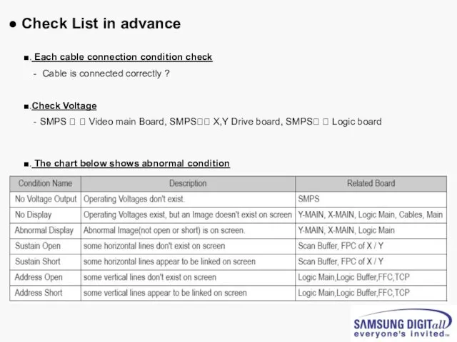
● Check List in advance
■. Each cable connection condition check
● Check List in advance
■. Each cable connection condition check
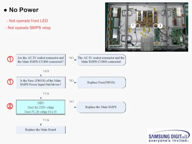
● No Power
- Not operate front LED
Not operate SMPS relay
①
①
②
1
2
● No Power
- Not operate front LED
Not operate SMPS relay
①
①
②
1
2
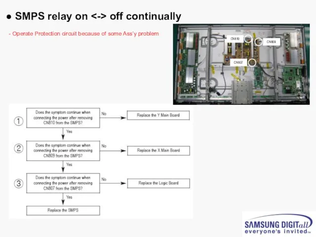
● SMPS relay on <-> off continually
Operate Protection circuit
● SMPS relay on <-> off continually
Operate Protection circuit
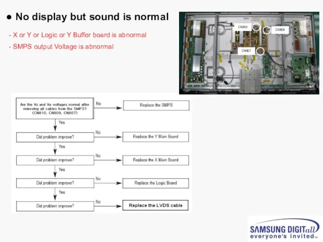
● No display but sound is normal
X or Y
● No display but sound is normal
X or Y
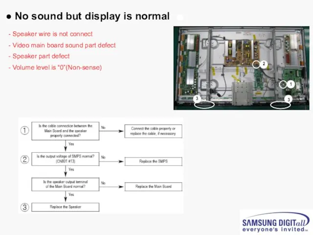
● No sound but display is normal
Speaker wire is
● No sound but display is normal
Speaker wire is
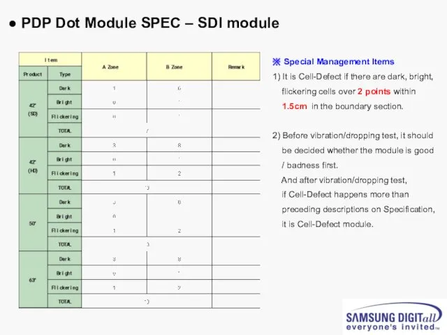
● PDP Dot Module SPEC – SDI module
※ Special Management Items
1)
● PDP Dot Module SPEC – SDI module
※ Special Management Items
1)
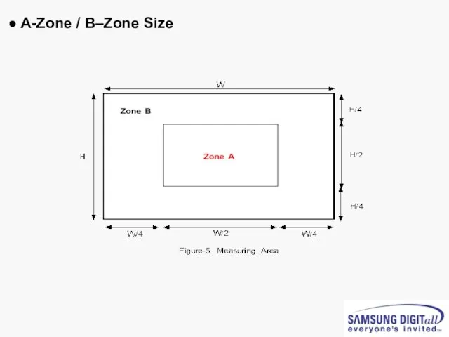
● A-Zone / B–Zone Size
● A-Zone / B–Zone Size
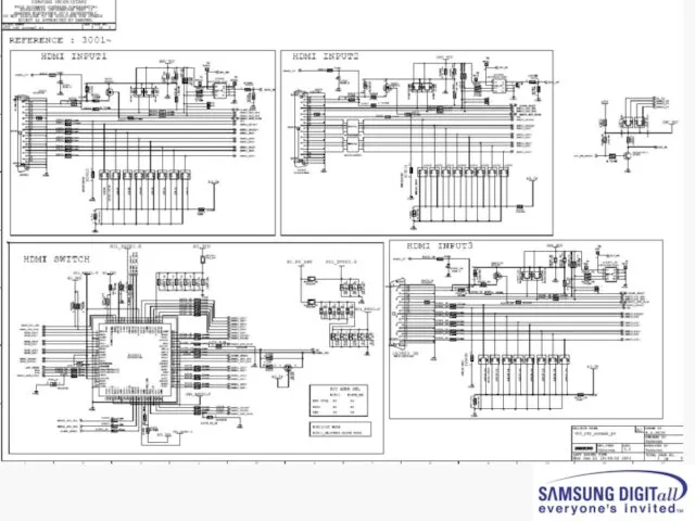
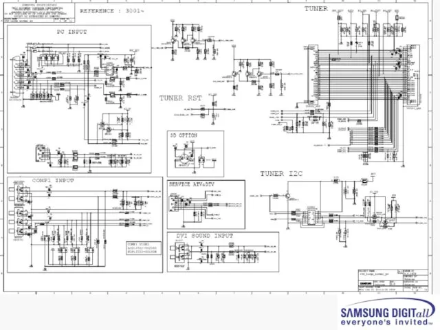
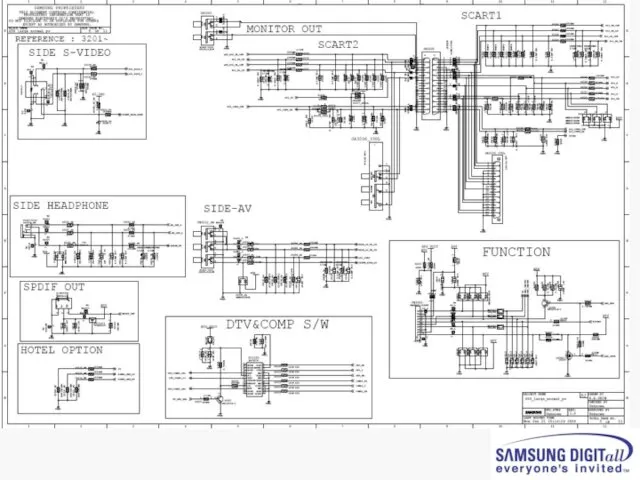
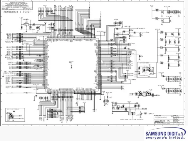
6.CIRCUIT DIAGRAM
6.CIRCUIT DIAGRAM
 Classical angular momentum and magnetic dipole moment
 Современные методы предотвращения явления помпажа в центробежных компрессорах
 Тайны невесомости
 Кристаллические и аморфные тела
 Простые механизмы и их использование в машинах
 Давление газа. Физика. 7 класс
 Батарейка. Гальванический элемент.
 Механічна енергія. Потенціальна і кінетична енергії тіла
 Модель двигателя Стирлинга
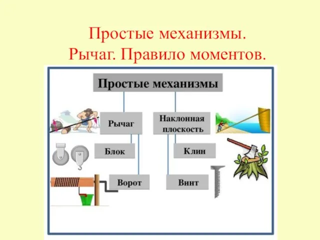 Простые механизмы. Рычаг. Правило моментов
 Методы наблюдения и регистрации элементарных частиц
 Закон Кулона. Электрическое поле
 Теплоизоляция теплообменных аппаратов
 Автоматика. Типовые звенья САУ и их свойства
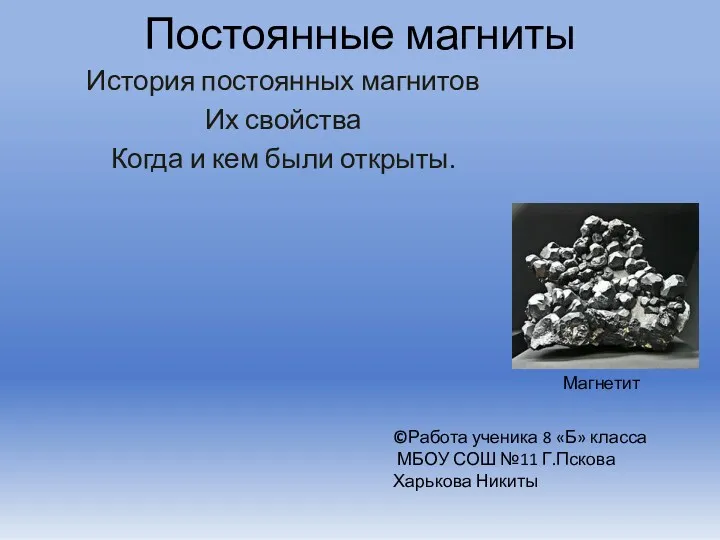 Постоянные магниты
 Внедрение ФГОС общего образования второго поколения по физике
 Игра Поле чудес по теме Нобелевские лауреаты по физике
 Автоматическая система капельного полива огорода с помощью солнечного нагрева воды
 Электрические заряды
 Химия-технологиялық процестерді модельдеу. Ұқсастық теориясының негіздері
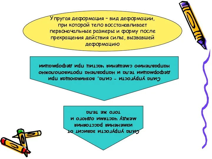 Упругая деформация
 Лазерные технологии и их использование
 Реле направления мощности
 Кинематика поступательного и вращательного движения
 Электромагнитная индукция. Индуктивность проводников. Энергия магнитного поля
 Научные программы, реализующие метод молекулярной динамики. Программа XMD
 Станция управления приводов ШГН СКАД-0-УЗЭП. Устройство, диагностика и ремонт
 Момент силы относительно центра (точки)