- Классификация нано-объектов

Содержание
- 2. Учебный план. Часть 1 – механика нано-объектов в среде Механизмы формирование наносистем в твердых телах. Упругие
- 3. Учебный план. Часть 2 – нано-электро-механические системы Материалы и технология изготовления нано-электро-механических систем. Элементы нано-электро-механических систем.
- 4. Литература Основная Cleland A.N. “Foundations of Nanomechanics” (Springer-Verlag, Berlin, Heidelberg, New York, 2003). Freund L.B., Suresh
- 5. Классификация нано-объектов пленка или слой нить или проволока островок или точка 1D 2D 0D
- 6. Пример: вертикально излучающий лазер vertical cavity surface emitting laser (VCSEL) (a) Schematic of the vertical cavity
- 7. Пример: нано-электро-механические системы (НЭМС) Electron micrographs of silicon NEMS structures made by surface micromachining and e-beam
- 8. Формирование наноструктур Эпитаксия, наращивание, напыление Само-организация на поверхности или в объеме Литография и травление
- 9. Планарные технологии
- 10. Напыление – Sputtering, Physical deposition
- 11. Напыление Бомбардировка ионами, возможно в присутствии внешних полей: СВЧ, магнетронное, и др. Распыляемая мишень осаждается на
- 12. Молекулярно-пучковая (лучевая) эпитаксия – molecular-beam epitaxy (MBE) Схема типичной промышленной установки
- 13. Процессы на поверхности при МПЭ
- 14. Газофазная эпитаксия (Vapor Phase Epitaxy) в хлоридной системе или с использованием металло-органических соединений metal-organic chemical vapor
- 15. Процессы на поверхности при MOCVD Процессы, происходящие при MOCVD
- 16. Моды эпитаксиального роста Технология молекулярно-лучевой эпитаксии (MBE) или газофазной эпитаксии с использованием металлоорганических соединений (MOVPE, MOCVD).
- 17. Движущая сила эпитаксии – пересыщение (supersaturation) газовой фазы и адсорбционного слоя ΔF = kTv ln(p/pe), where
- 18. Само-организация
- 19. Три стадии формирования наночастиц Нуклеация (Nucleation) - Гомогенное или гетерогенное образование зародышей новой фазы за счет
- 20. Поверхностная энергия γ > 0 – коэффициент поверхностного натяжения S – площадь поверхности Формирование частицы новой
- 21. Нуклеация в объеме Работа, необходимая для создания зародыша новой фазы Критический зародыш Вероятность образования зародыша новой
- 22. Нуклеация островка на поверхности Young 1805 θ > 0 – распад пленки на островки (Volmer -
- 23. Нуклеация при пересыщении на поверхности
- 24. Давление под искривленной поверхностью Для двух фаз, находящихся в равновесии, γ = 1 Дж/м2 k =
- 25. Самоорганизация при пересыщении на поверхности Выращивание субмонослойных островков Распад тонких пленок на островки Выращивание усов (whiskers,
- 26. Механизм роста ПЖК Пересыщенный пар кристаллическая подложка пересыщенная жидкость кристалл ус whisker nanowire nanorod
- 27. ZnO nanowires on sapphire (a) Plan view and (b) glancing view of ZnO nanowires grown on
- 28. ZnO nanostructures Typical SEM images showing morphologies of ZnO structures: dense filmlike rods (a), dense filmlike
- 29. Одномерные наноструктуры G H I J A schematic summary of the kinds of quasi-one dimensional nanostructures:
- 30. Synthesis of core–shell nanowires a, Gaseous reactants (red) catalytically decompose on the surface of a gold
- 31. Si–Si homoepitaxial core–shell nanowires. a, b, Diffraction contrast and highresolution TEM images, respectively, of an unannealed
- 32. Ge–Si core–shell nanowires
- 33. Si–Ge and Si–Ge–Si core–shell nanowires. Elemental mapping cross-section indicating a 21-nm-diameter Si core (blue circles), 10-nm
- 34. Coaxially-gated nanowire transistors a, Device schematic showing transistor structure. The inset shows the cross-section of the
- 36. Скачать презентацию
 Анализ переходных процессов операторным методом. Уравнения электромагнитного поля. (Лекция 5)
 Урок 8 класс
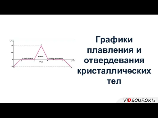 Графики плавления и отвердевания кристаллических тел
 Рекомендации по выбору посадок
 Крутые машины
 Резание металла слесарной ножовкой
 Електричне коло та його основні елементи
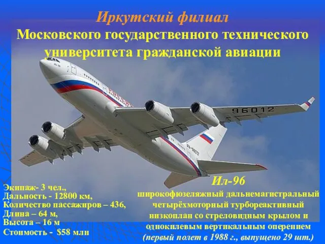
 Авиационные двигатели
 Свободное падение. (10 класс)
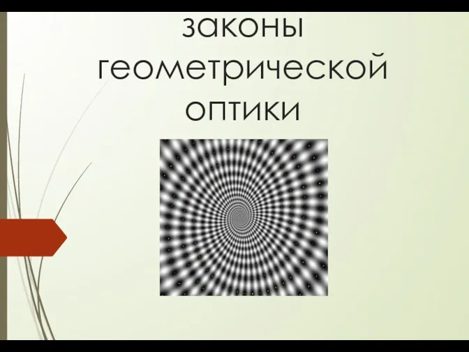 Законы геометрической оптики
 Организация технического обслуживания и ремонта автомобиля ГАЗ 3308 Садко
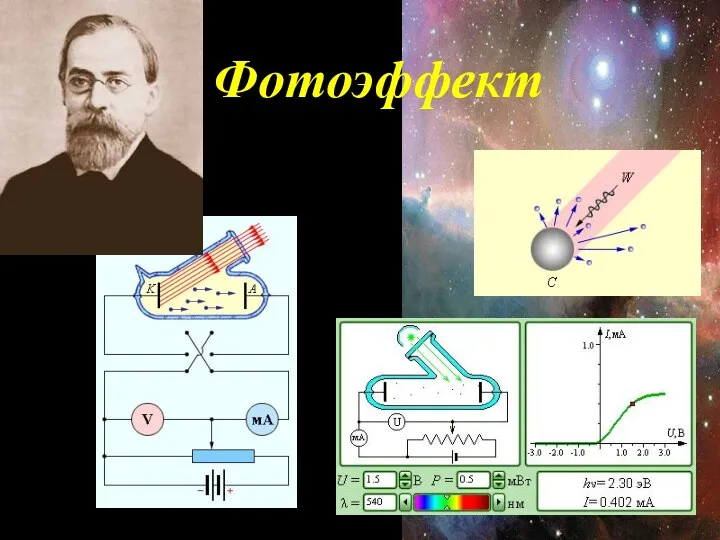 Фотоэффект. Раздел современной физики
 Фрикционные передачи
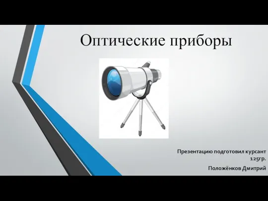 Оптические приборы
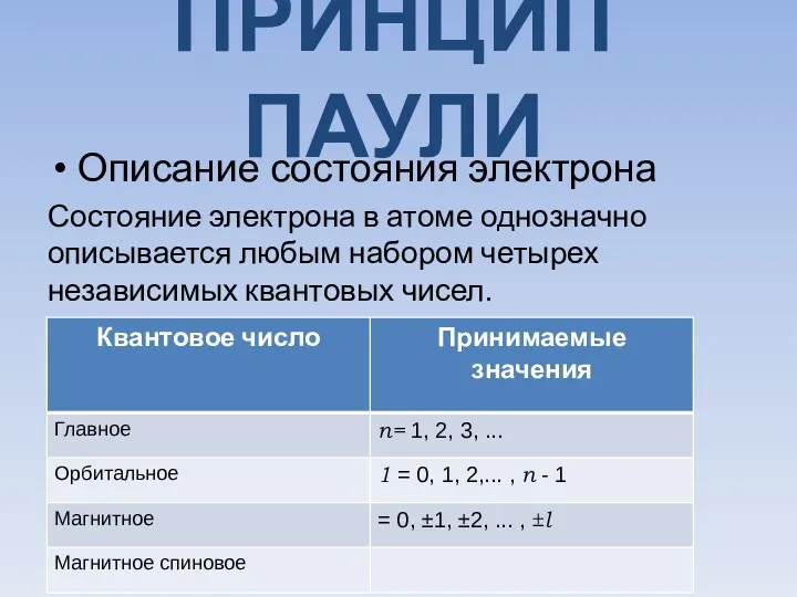 Принцип Паули
 Сила Лоренца
 Эрнест Уолтон и Джон Кокрофт
 Изготовление столярного соединения УС-1
 Электромагнитное поле
 Разработка урока по теме: Деление ядер урана. Цепная ядерная реакция. Термоядерные реакции.
 модели атомов
 Отражение и преломление света. Презентация.
 Внешний вид РУ и сборка 0,4/0,23 кВ
 Розв’язування задач з теми Закон збереження імпульсу
 Электрические явления в природе
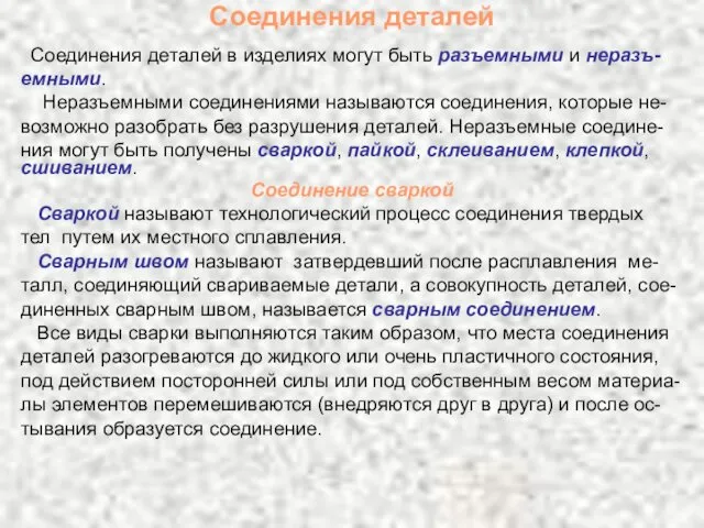 Соединения деталей. Соединения неразъемные
 Презентация по теме Второй закон Ньютона
 Презентация для урока по теме Изопроцессы в газах