- Placement and routing guidelines for Power Electronics Devices

Содержание
- 2. Lecture plan Planning the layout. Single-board PCB layout. Placement of Layers for PE devices. Current loops
- 3. Current position: 1/7 Planning the layout. Single-board PCB layout. Placement of Layers for PE devices. Current
- 4. PCB design for PE devices. Why is it so important? Improper PCB design leads to: "unstable"
- 5. Planning the layout. Each PE device contains power part and control scheme. Power part - DC/DC,
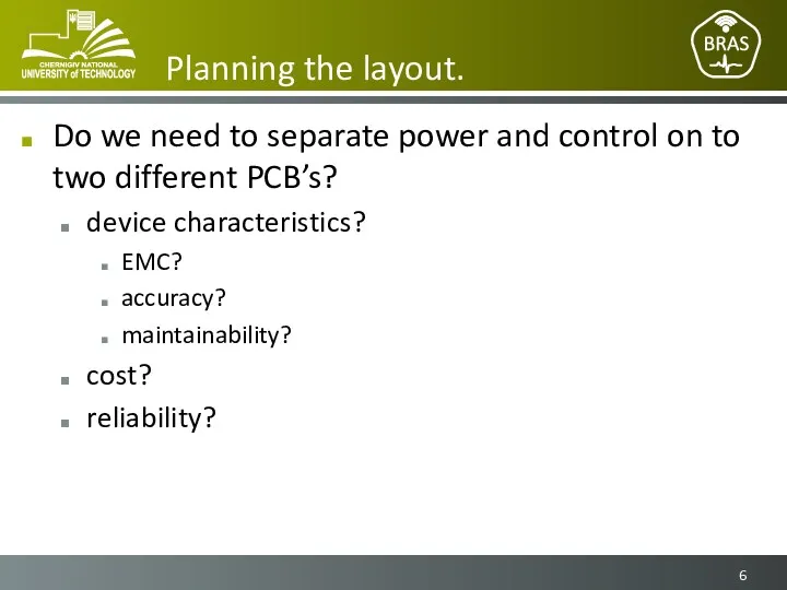
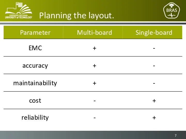
- 6. Planning the layout. Do we need to separate power and control on to two different PCB’s?
- 7. Planning the layout.
- 8. Current position: 2/7 Planning the layout. Single-board PCB layout. Placement of Layers for PE devices. Current
- 9. Single-board PCB layout. Power part location should be done at the first stage of PCB layout.
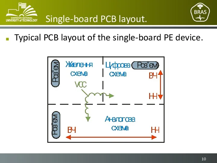
- 10. Single-board PCB layout. Typical PCB layout of the single-board PE device.
- 11. Single-board PCB layout. High speed components (both analog and digital) need to be placed as close
- 12. Current position: 3/7 Planning the layout. Single-board PCB layout. Placement of Layers for PE devices. Current
- 13. Stack of layers – 1, 2 or more? 1-layer PCB: Most sensitive to crosstalk and another
- 14. Stack of layers – 1, 2 or more? Multi-layer PCB: Better than 2-layer – more space
- 15. Stack of layers – 1, 2 or more? Conclusion: 1-layer PCBs – exceptional cases. 2-layer PCBs
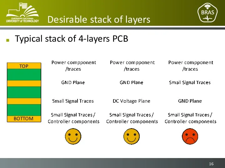
- 16. Desirable stack of layers Typical stack of 4-layers PCB
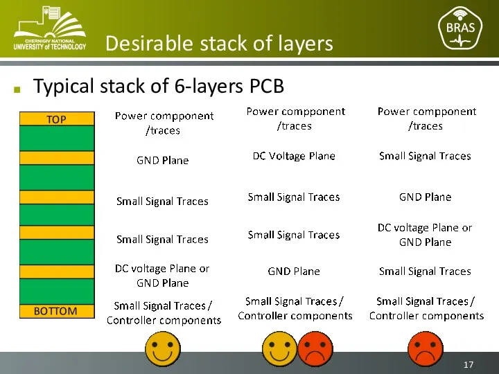
- 17. Desirable stack of layers Typical stack of 6-layers PCB
- 18. Current position: 4/7 Planning the layout. Single-board PCB layout. Placement of Layers for PE devices. Current
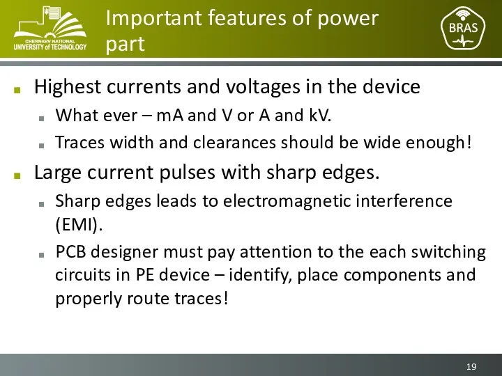
- 19. Important features of power part Highest currents and voltages in the device What ever – mA
- 20. Buck Converter
- 21. Current loops ordered by EMI generation in power conv. 1. Power switch loop – maximum attention!
- 22. Boost converter
- 23. Transformer Isolated Flyback Converter
- 24. The first rule for PE devices PCB design. 1. The pulse loop circumference must be as
- 25. PCB layout for buck converter. Red – power switch loop, blue – rectifier loop. cross select
- 26. Red – rectifier loop, black – load loop. Output Rectifier Loop in Flyback Converter
- 27. Parallel C Filter Layout
- 28. Parallel C Filter Layout PCB layout between each capacitor and source in multi-component filter must be
- 29. Current position: 5/7 Planning the layout. Single-board PCB layout. Placement of Layers for PE devices. Current
- 30. Grounding in the PE devices. Types of ground in power convertor devices: Power ground with high
- 31. Grounding in buck converter Red – control ground, blue – power ground.
- 32. Control and power ground connection. Rules of thumb for grounding in PE devices: Feedback ground must
- 33. Grounding in flyback converter
- 34. Current position: 6/7 Planning the layout. Single-board PCB layout. Placement of Layers for PE devices. Current
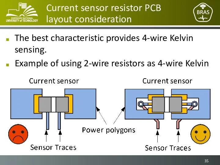
- 35. Current sensor resistor PCB layout consideration The best characteristic provides 4-wire Kelvin sensing. Example of using
- 36. Current sensor resistor PCB layout consideration Sensing trace should be placed on opposite layer and connect
- 37. Land Patterns for SMD components in PE devices For minimization of ESL and ESR Pad configuration
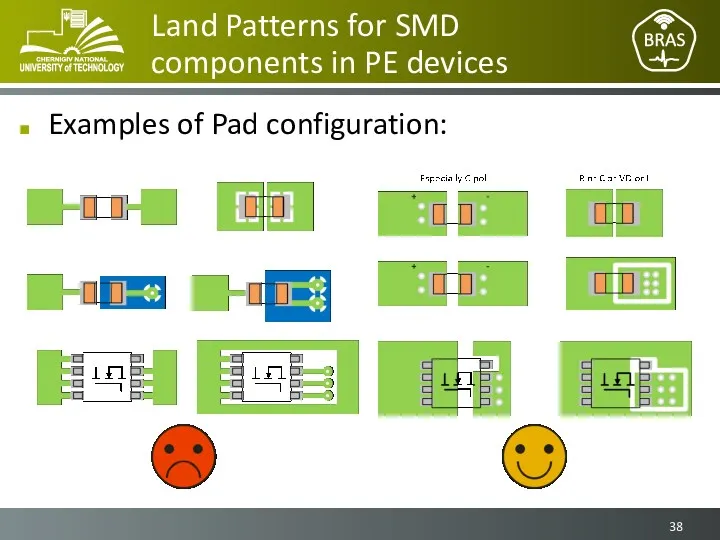
- 38. Land Patterns for SMD components in PE devices Examples of Pad configuration:
- 39. Current position: 7/7 Planning the layout. Single-board PCB layout. Placement of Layers for PE devices. Current
- 40. Mixed-signal grounding Mixed-signal components: External DAC and ADC, MCU with DAC/ADC on board. Ground in mixed-signal
- 41. Mixed-signal grounding Mixed-signal components: External DAC and ADC, MCU with DAC/ADC on board. Ground in mixed-signal
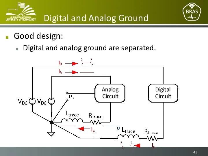
- 42. Digital and Analog Ground Bed design: Digital (“dirty”) and analog (“clean”) ground are common – AGND
- 43. Digital and Analog Ground Good design: Digital and analog ground are separated.
- 44. Digital and Analog Ground Planes for ground in control circuits of power electronic devices should improve
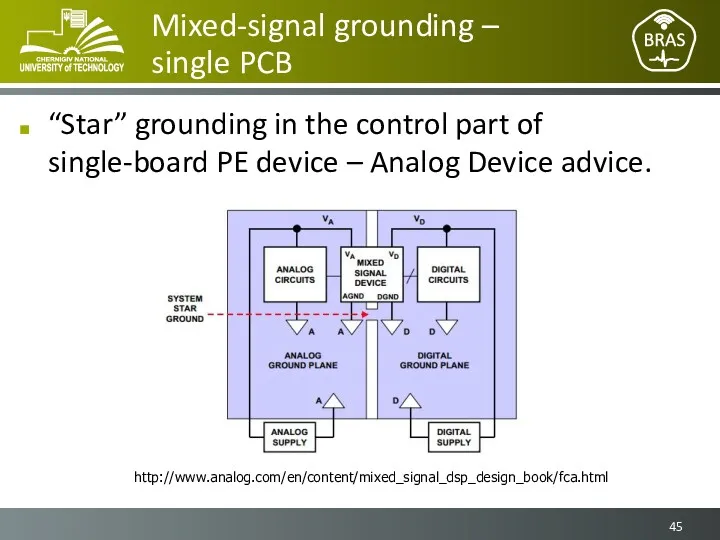
- 45. Mixed-signal grounding – single PCB “Star” grounding in the control part of single-board PE device –
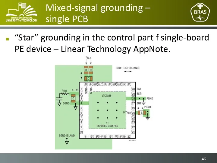
- 46. Mixed-signal grounding – single PCB “Star” grounding in the control part f single-board PE device –
- 47. Mixed-signal grounding – multi-board PCB Grounding techniques for single-board PE devices are not optimum for multi-board
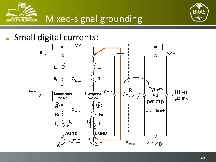
- 48. Mixed-signal grounding Small digital currents:
- 49. Mixed-signal grounding Small digital currents: http://www.analog.com/en/content/mixed_signal_dsp_design_book/fca.html
- 50. Mixed-signal grounding High digital currents: http://www.analog.com/en/content/mixed_signal_dsp_design_book/fca.html
- 51. Bypass Capacitors Noise on power line caused by switching digital components is shunted through the bypass
- 52. Bypass Capacitors Bypass capacitor should be connected to the power pins of the digital components as
- 54. Скачать презентацию
Lecture plan
Planning the layout.
Single-board PCB layout.
Placement of Layers for PE devices.
Current
Lecture plan
Planning the layout.
Single-board PCB layout.
Placement of Layers for PE devices.
Current
Current position: 1/7
Planning the layout.
Single-board PCB layout.
Placement of Layers for PE
Current position: 1/7
Planning the layout.
Single-board PCB layout.
Placement of Layers for PE
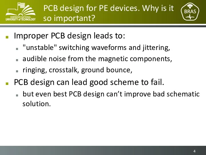
PCB design for PE devices. Why is it so important?
Improper PCB
PCB design for PE devices. Why is it so important?
Improper PCB
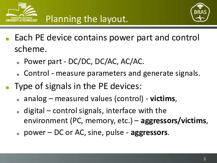
Planning the layout.
Each PE device contains power part and control scheme.
Power
Planning the layout.
Each PE device contains power part and control scheme.
Power
Planning the layout.
Do we need to separate power and control on
Planning the layout.
Do we need to separate power and control on
Planning the layout.
Planning the layout.
Current position: 2/7
Planning the layout.
Single-board PCB layout.
Placement of Layers for PE
Current position: 2/7
Planning the layout.
Single-board PCB layout.
Placement of Layers for PE
Single-board PCB layout.
Power part location should be done at the first
Single-board PCB layout.
Power part location should be done at the first
Single-board PCB layout.
Typical PCB layout of the single-board PE device.
Single-board PCB layout.
Typical PCB layout of the single-board PE device.
Single-board PCB layout.
High speed components (both analog and digital) need to
Single-board PCB layout.
High speed components (both analog and digital) need to
Current position: 3/7
Planning the layout.
Single-board PCB layout.
Placement of Layers for PE
Current position: 3/7
Planning the layout.
Single-board PCB layout.
Placement of Layers for PE
Stack of layers – 1, 2 or more?
1-layer PCB:
Most sensitive to
Stack of layers – 1, 2 or more?
1-layer PCB:
Most sensitive to
Stack of layers – 1, 2 or more?
Multi-layer PCB:
Better than 2-layer
Stack of layers – 1, 2 or more?
Multi-layer PCB:
Better than 2-layer
Stack of layers – 1, 2 or more?
Conclusion:
1-layer PCBs – exceptional
Stack of layers – 1, 2 or more?
Conclusion:
1-layer PCBs – exceptional
Desirable stack of layers
Typical stack of 4-layers PCB
Desirable stack of layers
Typical stack of 4-layers PCB
Desirable stack of layers
Typical stack of 6-layers PCB
Desirable stack of layers
Typical stack of 6-layers PCB
Current position: 4/7
Planning the layout.
Single-board PCB layout.
Placement of Layers for PE
Current position: 4/7
Planning the layout.
Single-board PCB layout.
Placement of Layers for PE
Important features of power part
Highest currents and voltages in the device
What
Important features of power part
Highest currents and voltages in the device
What
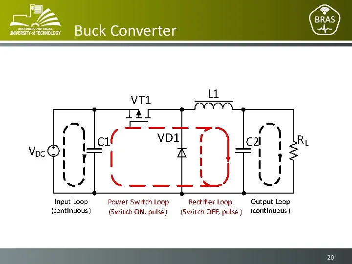
Buck Converter
Buck Converter
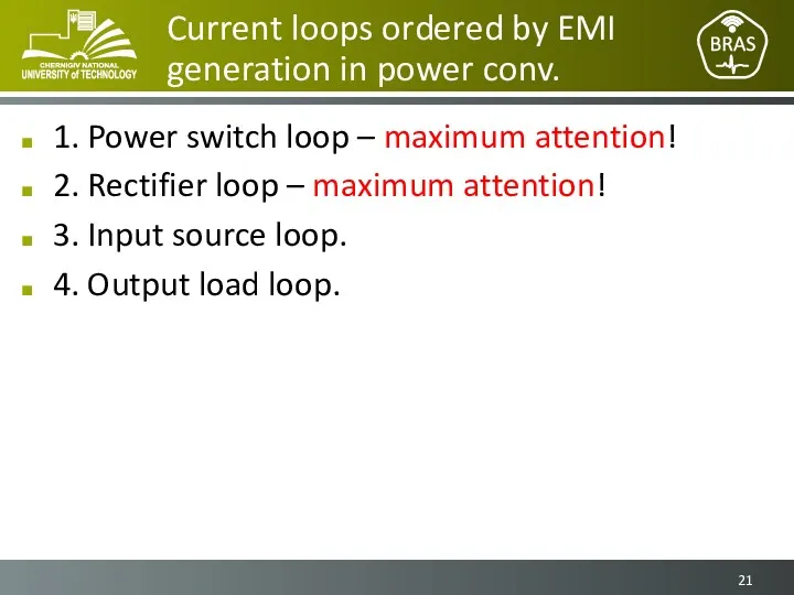
Current loops ordered by EMI generation in power conv.
1. Power switch
Current loops ordered by EMI generation in power conv.
1. Power switch
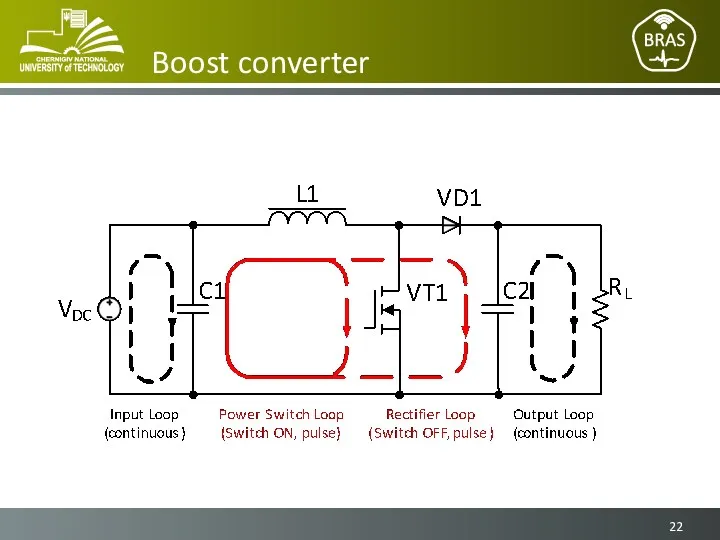
Boost converter
Boost converter
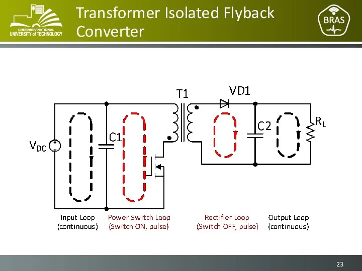
Transformer Isolated Flyback Converter
Transformer Isolated Flyback Converter
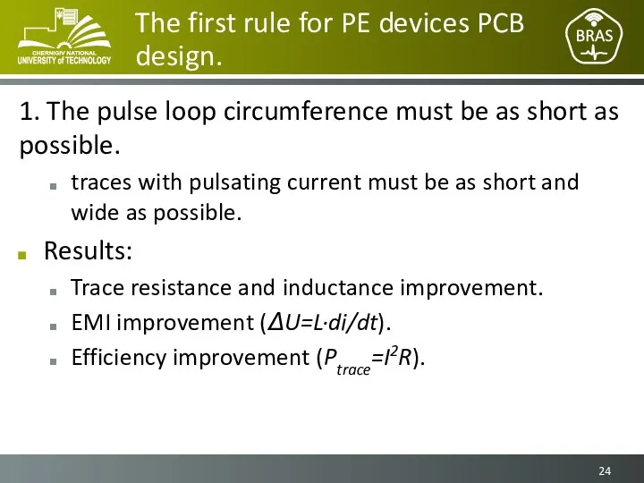
The first rule for PE devices PCB design.
1. The pulse loop
The first rule for PE devices PCB design.
1. The pulse loop
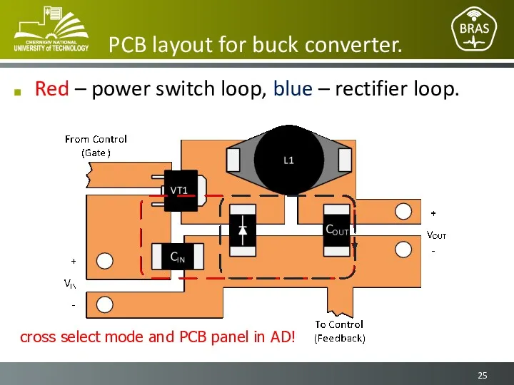
PCB layout for buck converter.
Red – power switch loop, blue –
PCB layout for buck converter.
Red – power switch loop, blue –
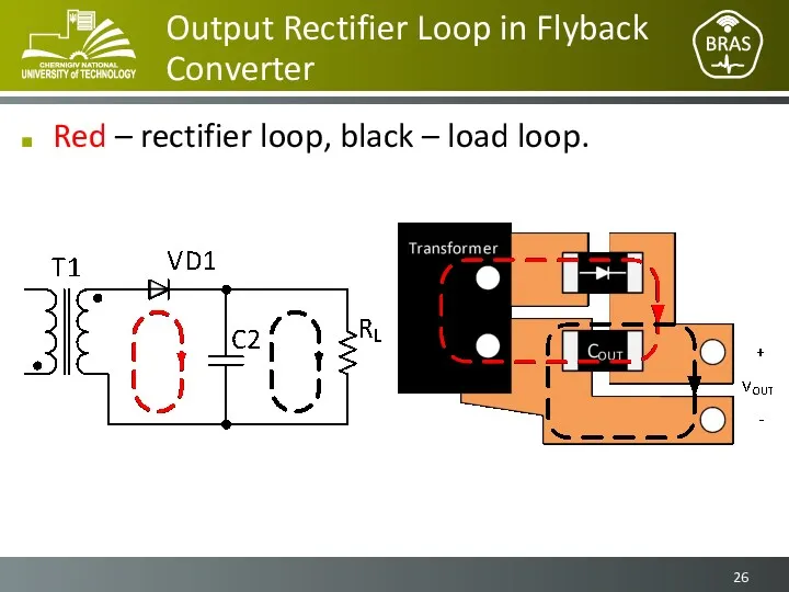
Red – rectifier loop, black – load loop.
Output Rectifier Loop
Red – rectifier loop, black – load loop.
Output Rectifier Loop
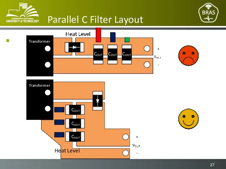
Parallel C Filter Layout
Parallel C Filter Layout
Parallel C Filter Layout
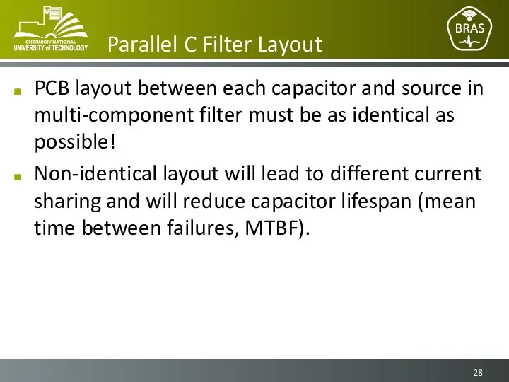
PCB layout between each capacitor and source in
Parallel C Filter Layout
PCB layout between each capacitor and source in
Current position: 5/7
Planning the layout.
Single-board PCB layout.
Placement of Layers for PE
Current position: 5/7
Planning the layout.
Single-board PCB layout.
Placement of Layers for PE
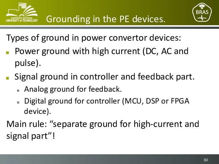
Grounding in the PE devices.
Types of ground in power convertor devices:
Power
Grounding in the PE devices.
Types of ground in power convertor devices:
Power
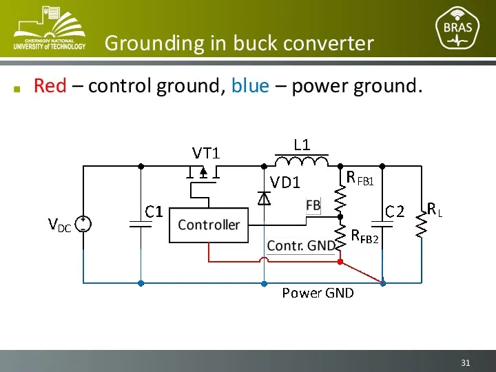
Grounding in buck converter
Red – control ground, blue – power ground.
Grounding in buck converter
Red – control ground, blue – power ground.
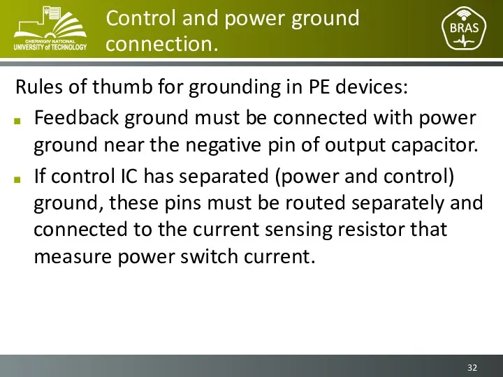
Control and power ground connection.
Rules of thumb for grounding in PE
Control and power ground connection.
Rules of thumb for grounding in PE
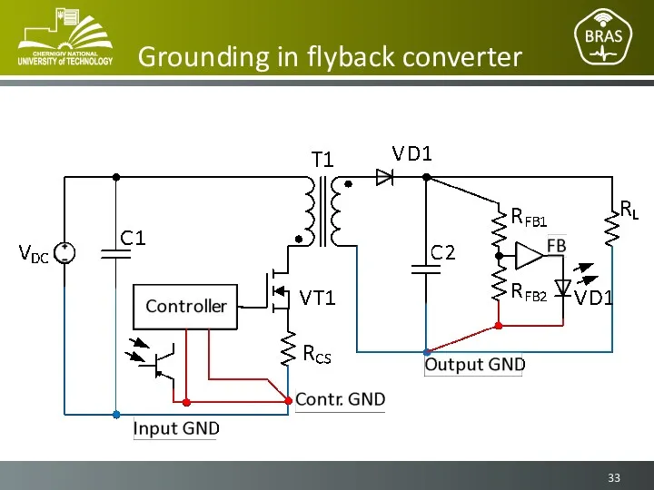
Grounding in flyback converter
Grounding in flyback converter
Current position: 6/7
Planning the layout.
Single-board PCB layout.
Placement of Layers for PE
Current position: 6/7
Planning the layout.
Single-board PCB layout.
Placement of Layers for PE
Current sensor resistor PCB layout consideration
The best characteristic provides 4-wire Kelvin
Current sensor resistor PCB layout consideration
The best characteristic provides 4-wire Kelvin
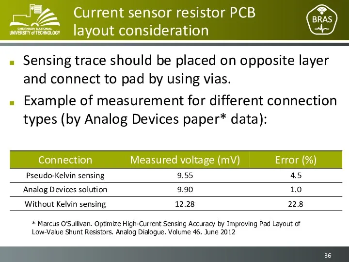
Current sensor resistor PCB layout consideration
Sensing trace should be placed on opposite
Current sensor resistor PCB layout consideration
Sensing trace should be placed on opposite
Land Patterns for SMD components in PE devices
For minimization of ESL
Land Patterns for SMD components in PE devices
For minimization of ESL
Land Patterns for SMD components in PE devices
Examples of Pad configuration:
Land Patterns for SMD components in PE devices
Examples of Pad configuration:
Current position: 7/7
Planning the layout.
Single-board PCB layout.
Placement of Layers for PE
Current position: 7/7
Planning the layout.
Single-board PCB layout.
Placement of Layers for PE
Mixed-signal grounding
Mixed-signal components:
External DAC and ADC, MCU with DAC/ADC on board.
Ground
Mixed-signal grounding
Mixed-signal components:
External DAC and ADC, MCU with DAC/ADC on board.
Ground

Mixed-signal grounding
Mixed-signal components:
External DAC and ADC, MCU with DAC/ADC on board.
Ground
Mixed-signal grounding
Mixed-signal components:
External DAC and ADC, MCU with DAC/ADC on board.
Ground
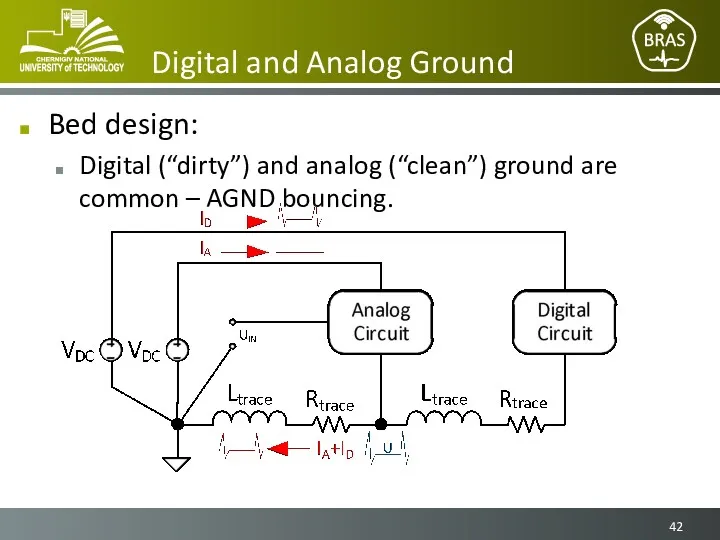
Digital and Analog Ground
Bed design:
Digital (“dirty”) and analog (“clean”) ground are
Digital and Analog Ground
Bed design:
Digital (“dirty”) and analog (“clean”) ground are
Digital and Analog Ground
Good design:
Digital and analog ground are separated.
Digital and Analog Ground
Good design:
Digital and analog ground are separated.
Digital and Analog Ground
Planes for ground in control circuits of power
Digital and Analog Ground
Planes for ground in control circuits of power
Mixed-signal grounding –
single PCB
“Star” grounding in the control part of
Mixed-signal grounding –
single PCB
“Star” grounding in the control part of
Mixed-signal grounding –
single PCB
“Star” grounding in the control part f
Mixed-signal grounding –
single PCB
“Star” grounding in the control part f
Mixed-signal grounding –
multi-board PCB
Grounding techniques for single-board PE devices are
Mixed-signal grounding –
multi-board PCB
Grounding techniques for single-board PE devices are
Mixed-signal grounding
Small digital currents:
Mixed-signal grounding
Small digital currents:
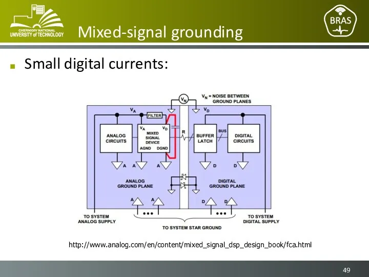
Mixed-signal grounding
Small digital currents:
http://www.analog.com/en/content/mixed_signal_dsp_design_book/fca.html
Mixed-signal grounding
Small digital currents:
http://www.analog.com/en/content/mixed_signal_dsp_design_book/fca.html
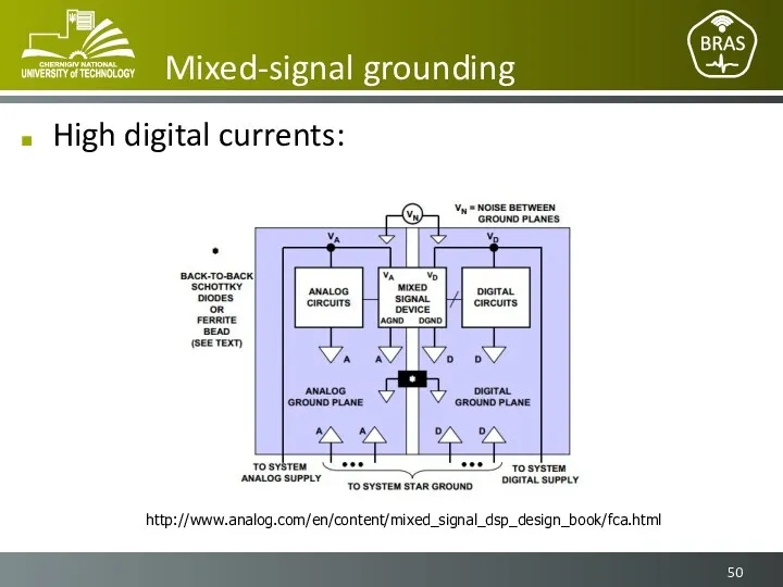
Mixed-signal grounding
High digital currents:
http://www.analog.com/en/content/mixed_signal_dsp_design_book/fca.html
Mixed-signal grounding
High digital currents:
http://www.analog.com/en/content/mixed_signal_dsp_design_book/fca.html
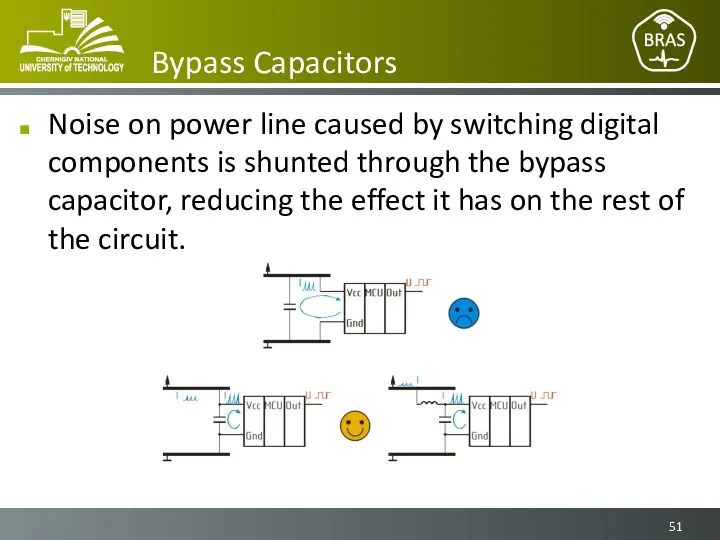
Bypass Capacitors
Noise on power line caused by switching digital components is
Bypass Capacitors
Noise on power line caused by switching digital components is
Bypass Capacitors
Bypass capacitor should be connected to the power pins of
Bypass Capacitors
Bypass capacitor should be connected to the power pins of
 Развивающие компьютерные игры для детей
 Проектирование информационных систем. Обследование и анализ информационной системы предприятия. (Лекция 1)
 Mac OS — семейство операционных систем производства корпорации Apple
 Учет межпредметных связей на уроках информатики
 Инструкция подключения учеников к видеоконференции через программу ZOOM
 Урок по созданию диаграмм в Excel для финансовых отчетов
 Види і типи сайтів. Цільова аудиторія (урок 1)
 Презентация У истоков компьютерной революции
 Тестирование и жизненный цикл ПО. CMM. Лекция 2
 Путешествие в страну информатики
 Действия с информацией. Тест
 Классы вычислительных машин (тема 1.1)
 Как создать свой сайт?
 Кодирование текстовой информации
 Общие сведения о языке программирования Паскаль. Начала программирования. Информатика. 8 класс
 Аддитивные технологии
 Разработка информационной системы для учета продаж билетов в авиакассах
 Введение в web-программирование
 Сапр AutoCAD - основные понятия и приемы работы
 Алгоритм создания и развития интернет ресурса
 Виды графики
 Интересные факты в сфере информационных технологий
 20231004_prilozhenie_1
 Компьютерные технологии в обучении: определение, разновидности, этапы
 Лайфхаки Word
 Алгоритмы и исполнители
 Все программы от Adobe
 Сеть Ethernet. Построение коммутируемой сети