- Field-effect transistor (FET). Junction field-effect transistor (JFET)

Содержание
- 2. Introduction (FET) Field-effect transistor (FET) are important devices such as BJTs Also used as amplifier and
- 3. Current-controlled amplifiers
- 4. Voltage-controlled amplifiers
- 5. High input impedance (MΩ) (Linear AC amplifier system) Temperature stable than BJT Smaller than BJT Can
- 6. Disadvantages of FET Easy to damage compare to BJT ???
- 7. There are 2 types of JFET n-channel JFET p-channel JFET Three Terminal gate: as in the
- 8. Junction field-effect transistor (JFET)
- 9. N channel JFET: Major structure is n-type material (channel) between embedded p-type material to form 2
- 10. N-channel JFET..
- 11. Drain Source Gate Structure of an N-channel JFET P-type substrate P N-channel The channel has carriers
- 12. Drain Source Gate P N-channel P-type substrate A negative gate voltage can push the carriers from
- 13. P channel JFET: Major structure is p-type material (channel) between embedded n-type material to form 2
- 14. P-channel JFET..
- 15. P P + - DC Voltage Source + - + - N N Operation of a
- 16. Water analogy for the JFET control mechanism
- 17. JFET Characteristic Curve To start, suppose VGS=0 Then, when VDS is increased, ID increases. Therefore, ID
- 18. ID versus VDS for VGS = 0 V. JFET Characteristic Curve
- 19. JFET for VGS = 0 V and 0 Channel becomes narrower as VDS is increased
- 20. Pinch-off (VGS = 0 V, VDS = VP).
- 21. Application of a negative voltage to the gate of a JFET.
- 22. JFET Characteristic Curve.. For negative values of VGS, the gate-to-channel junction is reverse biased even with
- 23. 0 VDS in Volts ID in mA VGS N-channel JFET drain family of characteristic curves This
- 24. n-Channel JFET characteristics curve with IDSS = 8 mA and VP = -4 V. JFET Characteristic
- 25. p-Channel JFET
- 26. p-Channel JFET characteristics with IDSS = 6 mA and VP = +6 V.
- 27. Characteristics for n-channel JFET
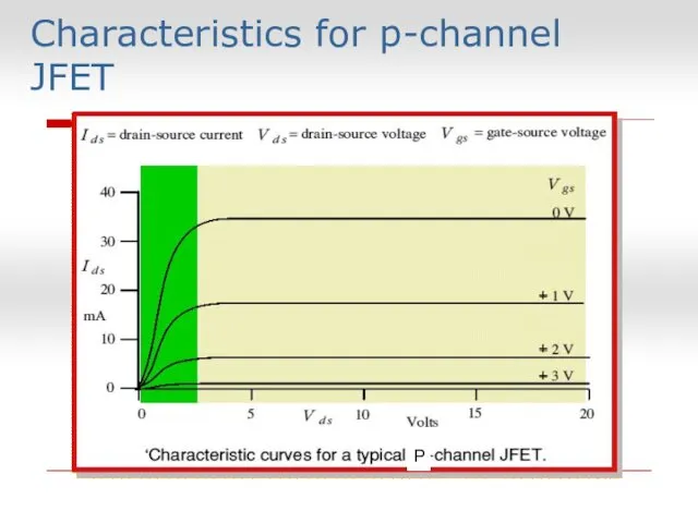
- 28. P + + + Characteristics for p-channel JFET
- 29. Operation of n-channel JFET JFET is biased with two voltage sources: VDD VGG VDD generate voltage
- 30. Transfer Characteristics The input-output transfer characteristic of the JFET is not as straight forward as it
- 31. Transfer Characteristics.. In JFET, the relationship between VGS (input voltage) and ID (output current) is used
- 32. Defined by Shockley’s equation: Relationship between ID and VGS. Obtaining transfer characteristic curve axis point from
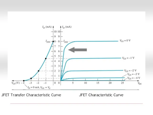
- 33. Transfer Characteristics JFET Transfer Characteristic Curve JFET Characteristic Curve
- 34. DC JFET Biasing Just as we learned that the BJT must be biased for proper operation,
- 35. Fixed-bias Fixed-bias + Vin _ + Vout _ + Use two voltage sources: VGG, VDD VGG
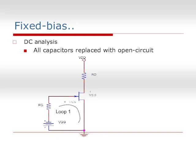
- 36. Fixed-bias.. DC analysis All capacitors replaced with open-circuit Loop 1
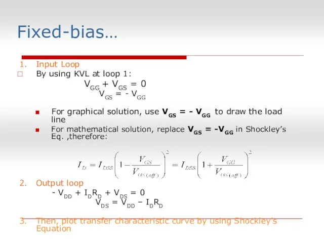
- 37. Fixed-bias… 1. Input Loop By using KVL at loop 1: VGG + VGS = 0 VGS
- 39. Скачать презентацию
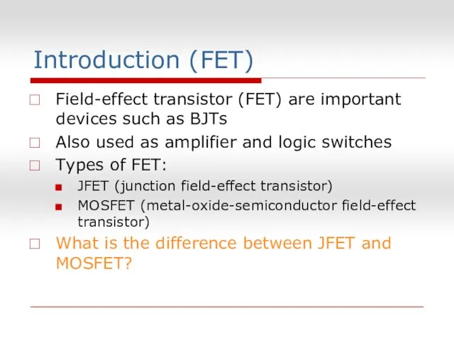
Introduction (FET)
Field-effect transistor (FET) are important devices such as BJTs
Also used
Introduction (FET)
Field-effect transistor (FET) are important devices such as BJTs
Also used
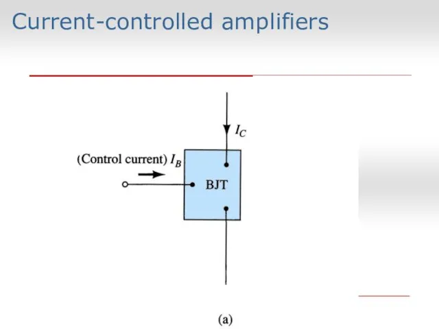
Current-controlled amplifiers
Current-controlled amplifiers
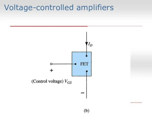
Voltage-controlled amplifiers
Voltage-controlled amplifiers
High input impedance (MΩ) (Linear AC amplifier system)
Temperature stable than BJT
Smaller
High input impedance (MΩ) (Linear AC amplifier system)
Temperature stable than BJT
Smaller
Disadvantages of FET
Easy to damage compare to BJT
???
Disadvantages of FET
Easy to damage compare to BJT
???
There are 2 types of JFET
n-channel JFET
p-channel JFET
Three Terminal
gate: as in
There are 2 types of JFET
n-channel JFET
p-channel JFET
Three Terminal
gate: as in
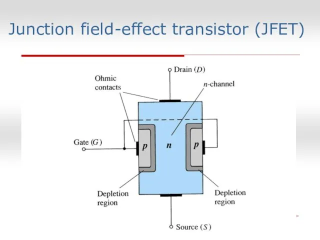
Junction field-effect transistor (JFET)
Junction field-effect transistor (JFET)
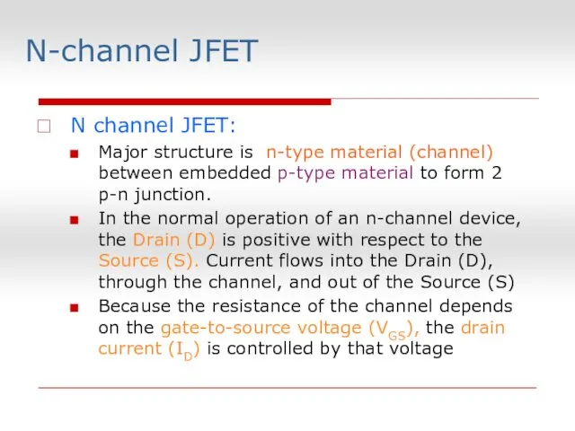
N channel JFET:
Major structure is n-type material (channel) between embedded p-type
N channel JFET:
Major structure is n-type material (channel) between embedded p-type
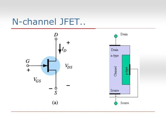
N-channel JFET..
N-channel JFET..
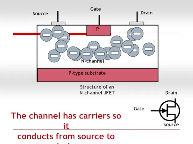
Drain
Source
Gate
Structure of an
N-channel JFET
P-type substrate
P
N-channel
The channel has carriers so it
conducts
Drain
Source
Gate
Structure of an
N-channel JFET
P-type substrate
P
N-channel
The channel has carriers so it
conducts
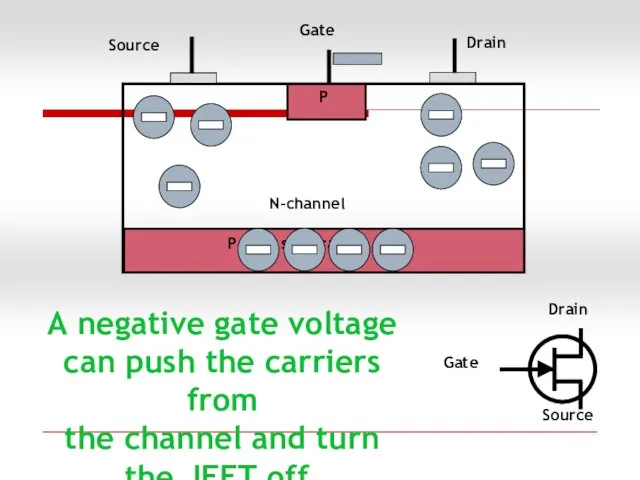
Drain
Source
Gate
P
N-channel
P-type substrate
A negative gate voltage
can push the carriers from
the channel and
Drain
Source
Gate
P
N-channel
P-type substrate
A negative gate voltage
can push the carriers from
the channel and
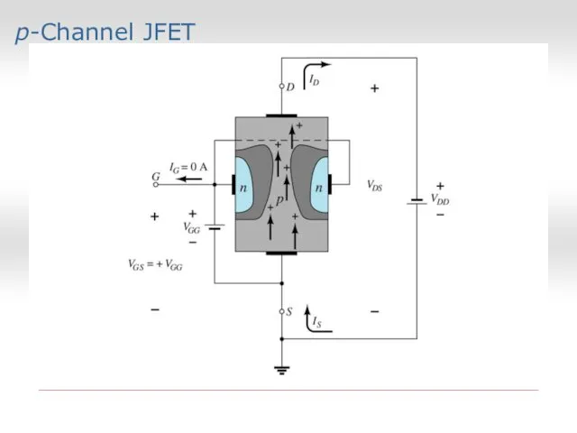
P channel JFET:
Major structure is p-type material (channel) between embedded n-type
P channel JFET:
Major structure is p-type material (channel) between embedded n-type
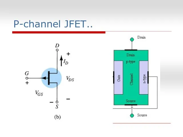
P-channel JFET..
P-channel JFET..

P
P
+
-
DC Voltage Source
+
-
+
-
N
N
Operation of a JFET
Gate
Drain
Source
P
P
+
-
DC Voltage Source
+
-
+
-
N
N
Operation of a JFET
Gate
Drain
Source
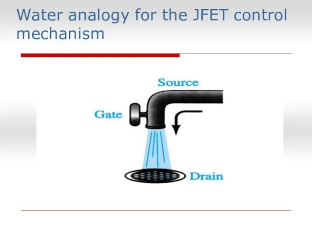
Water analogy for the JFET control mechanism
Water analogy for the JFET control mechanism
JFET Characteristic Curve
To start, suppose VGS=0
Then, when VDS is increased, ID
JFET Characteristic Curve
To start, suppose VGS=0
Then, when VDS is increased, ID
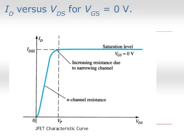
ID versus VDS for VGS = 0 V.
JFET Characteristic Curve
ID versus VDS for VGS = 0 V.
JFET Characteristic Curve
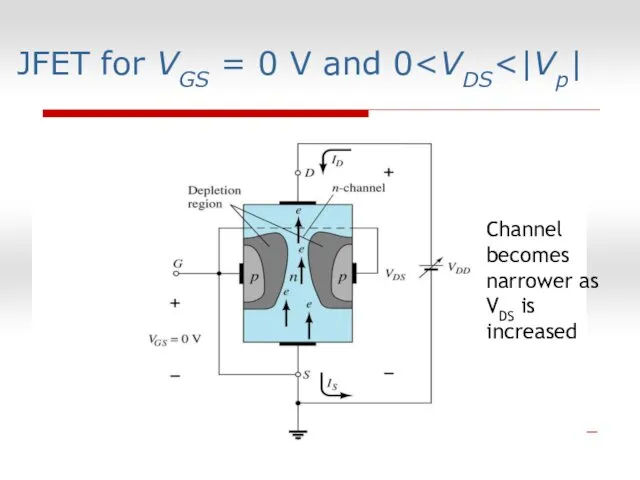
JFET for VGS = 0 V and 0Channel becomes narrower as
JFET for VGS = 0 V and 0 Channel becomes narrower as
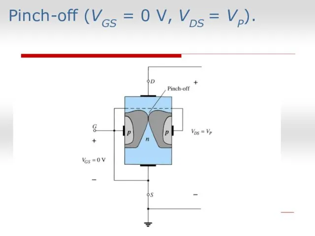
Pinch-off (VGS = 0 V, VDS = VP).
Pinch-off (VGS = 0 V, VDS = VP).
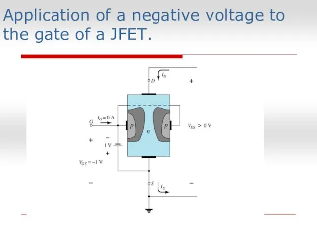
Application of a negative voltage to the gate of a JFET.
Application of a negative voltage to the gate of a JFET.
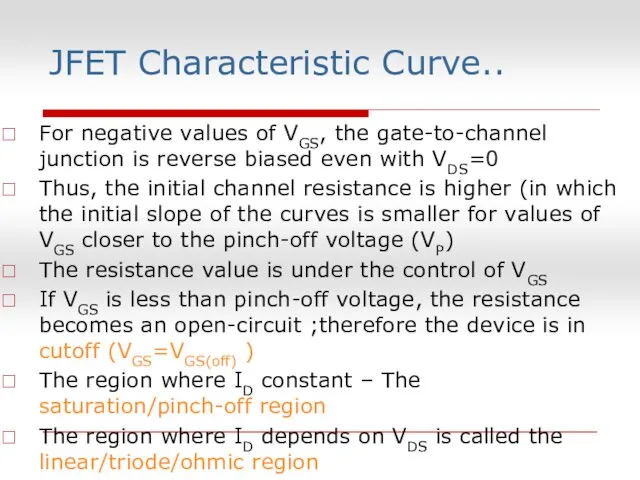
JFET Characteristic Curve..
For negative values of VGS, the gate-to-channel junction is
JFET Characteristic Curve..
For negative values of VGS, the gate-to-channel junction is

0
VDS in Volts
ID in mA
VGS
N-channel JFET drain family of characteristic curves
This
0
VDS in Volts
ID in mA
VGS
N-channel JFET drain family of characteristic curves
This
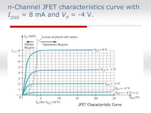
n-Channel JFET characteristics curve with IDSS = 8 mA and VP
n-Channel JFET characteristics curve with IDSS = 8 mA and VP
p-Channel JFET
p-Channel JFET
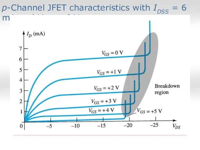
p-Channel JFET characteristics with IDSS = 6 mA and VP =
p-Channel JFET characteristics with IDSS = 6 mA and VP =
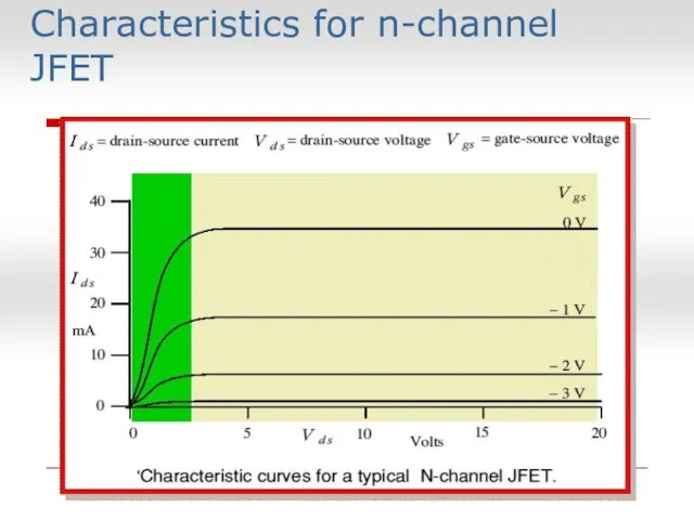
Characteristics for n-channel JFET
Characteristics for n-channel JFET
P
+
+
+
Characteristics for p-channel JFET
P
+
+
+
Characteristics for p-channel JFET
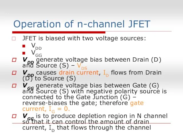
Operation of n-channel JFET
JFET is biased with two voltage sources:
VDD
VGG
VDD generate
Operation of n-channel JFET
JFET is biased with two voltage sources:
VDD
VGG
VDD generate
Transfer Characteristics
The input-output transfer characteristic of the JFET is not as
Transfer Characteristics
The input-output transfer characteristic of the JFET is not as
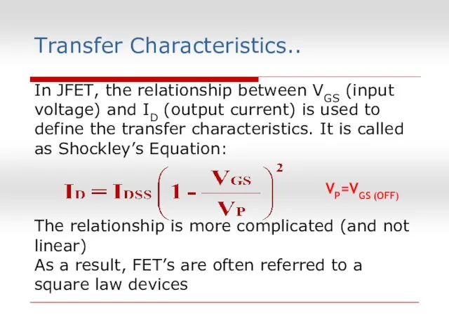
Transfer Characteristics..
In JFET, the relationship between VGS (input voltage) and ID
Transfer Characteristics..
In JFET, the relationship between VGS (input voltage) and ID
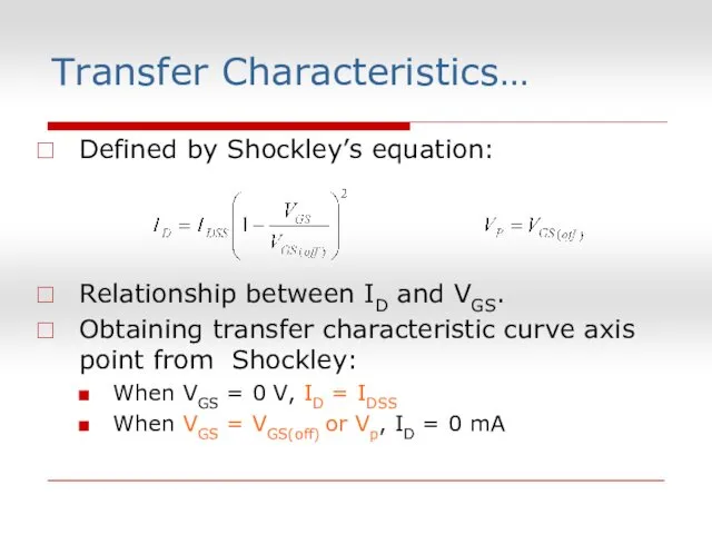
Defined by Shockley’s equation:
Relationship between ID and VGS.
Obtaining transfer characteristic curve
Defined by Shockley’s equation:
Relationship between ID and VGS.
Obtaining transfer characteristic curve
Transfer Characteristics
JFET Transfer Characteristic Curve
JFET Characteristic Curve
Transfer Characteristics
JFET Transfer Characteristic Curve
JFET Characteristic Curve
DC JFET Biasing
Just as we learned that the BJT must be
DC JFET Biasing
Just as we learned that the BJT must be
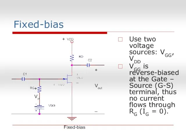
Fixed-bias
Fixed-bias
+
Vin
_
+
Vout
_
+
Use two voltage sources: VGG, VDD
VGG is reverse-biased at the Gate
Fixed-bias
Fixed-bias
+
Vin
_
+
Vout
_
+
Use two voltage sources: VGG, VDD
VGG is reverse-biased at the Gate
Fixed-bias..
DC analysis
All capacitors replaced with open-circuit
Loop 1
Fixed-bias..
DC analysis
All capacitors replaced with open-circuit
Loop 1
Fixed-bias…
1. Input Loop
By using KVL at loop 1:
VGG + VGS =
Fixed-bias…
1. Input Loop
By using KVL at loop 1:
VGG + VGS =
 Имена героев в названиях улиц города Советска
 Навесное оборудование для малогабиритной тяговой установки
 Сварочные выпрямители
 Аналитический обзор современных швейных машин потайного стежка
 Удостоверение сделок. Доверенность. Завещание и его формы
 Устройство карпового прудового рыбхоза
 Класс Пресмыкающиеся
 Парк флоры и фауны Роев ручей
 Поздравляем с Днём МАМ!
 Конкурс рисунков
 Призентация к общешкольному мероприятию 9 Мая- День Победы
 Наладка технологического оборудования на производстве
 Желаемые объекты Чкаловского парка
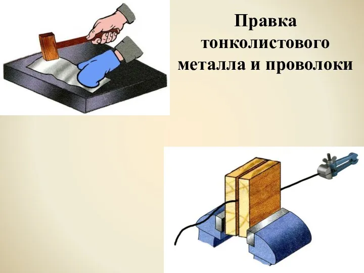 Правка тонколистового металла и проволоки. Проверь свои знания
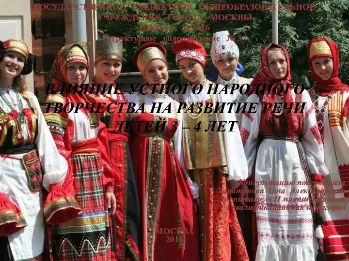 ВЛИЯНИЕ УСТНОГО НАРОДНОГО ТВОРЧЕСТВА НА РАЗВИТИЕ РЕЧИ ДЕТЕЙ 3 – 4 ЛЕТ.
 Логопедическое занятие для учащихся 3 класса (развитие связной речи) . Тема Плохо (по В. Осеевой)
 Блокада Ленинграда
 Проблемы корейского общества сквозь призму современной художественной литературы
 Презентация Православие и язычество на Руси.
 Презентация Нижний Новгород
 презентация Посуда
 Презентация кружка Волшебные краски часть 1
 Эмбриогенез человека
 Смутное время
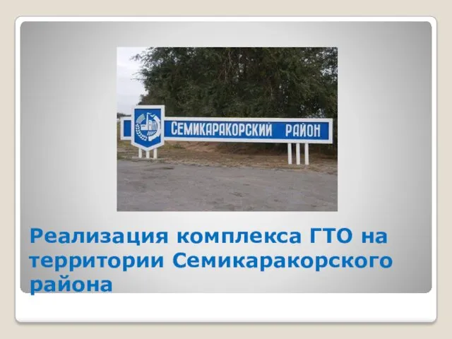 Реализация комплекса ГТО на территории Семикаракорского района
 Криминалистика как юридическая дисциплина
 Розвиток мовлення 4 клас ІІ семестр
 Международные отношения, мировая политика, внешняя политика и дипломатия в контексте новой научной парадигмы