- 1874 - Semiconductor Point-Contact Rectifier Effect Discovered

Содержание
- 2. 1930: Field Effect Semiconductor Device Concepts Patented Julius Lilienfeld filed a patent describing a three-electrode amplifying
- 3. 1940 - Discovery of the p-n Junction Russell Ohl and Jack Scaff at Bell Telephone Labs
- 4. By Bardeen, Brattain, and Shockley, Nobel Laureates in Physics 1956 1947 1947 - Invention of the
- 5. By Jack Kilby (TI), Nobel Laureates in Physics 2000 1958 - All semiconductor “Hybris Integrated Circuit"
- 6. 1959 - Practical Monolithic Integrated Circuit Concept Patented Robert Noyce Challenged by patent attorney to identify
- 7. 1960 - MOS Transistor Demonstrated John Atalla and Dawon Kahng at Bell demonstrate the first successful
- 8. 1963 - Complementary MOS Circuit Invented Frank Wanlass and C. T. Sah at Fairchild R &
- 9. 1965 - "Moore's Law" Predicts the Future of Integrated Circuits Electronics Magazine (April 1965) IEEE, IEDM
- 10. 1974 - Scaling of IC Process Design Rules Quantified Constant E Field Scaling All device parameters
- 12. Скачать презентацию
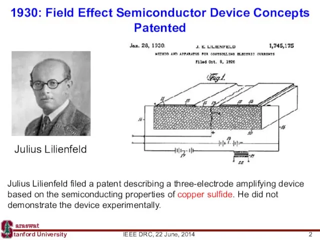
1930: Field Effect Semiconductor Device Concepts Patented
Julius Lilienfeld filed a patent
1930: Field Effect Semiconductor Device Concepts Patented
Julius Lilienfeld filed a patent
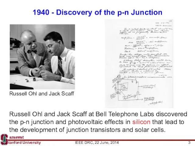
1940 - Discovery of the p-n Junction
Russell Ohl and Jack Scaff
1940 - Discovery of the p-n Junction
Russell Ohl and Jack Scaff
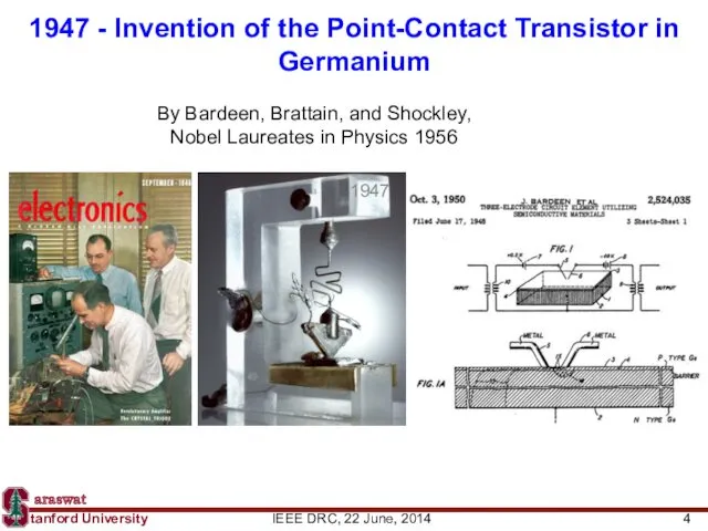
By Bardeen, Brattain, and Shockley, Nobel Laureates in Physics 1956
1947
1947 -
By Bardeen, Brattain, and Shockley, Nobel Laureates in Physics 1956
1947
1947 -
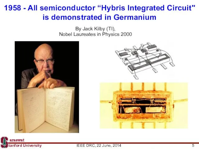
By Jack Kilby (TI),
Nobel Laureates in Physics 2000
1958 - All
By Jack Kilby (TI),
Nobel Laureates in Physics 2000
1958 - All
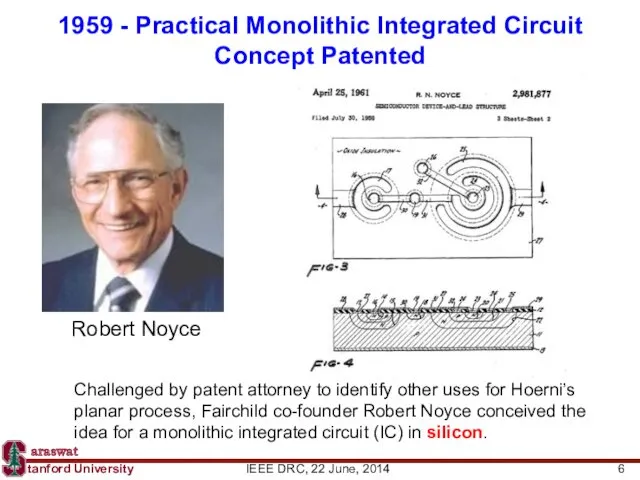
1959 - Practical Monolithic Integrated Circuit Concept Patented
Robert Noyce
Challenged by patent
1959 - Practical Monolithic Integrated Circuit Concept Patented
Robert Noyce
Challenged by patent
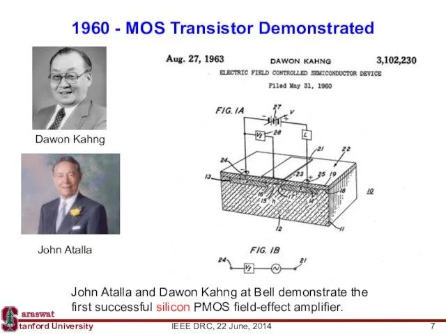
1960 - MOS Transistor Demonstrated
John Atalla and Dawon Kahng at Bell
1960 - MOS Transistor Demonstrated
John Atalla and Dawon Kahng at Bell
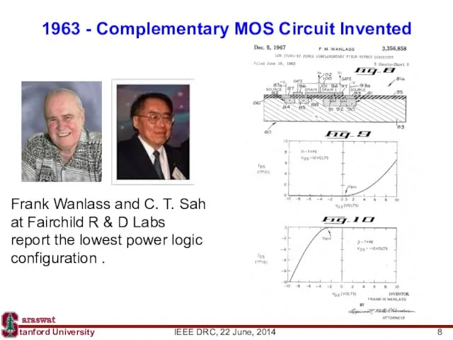
1963 - Complementary MOS Circuit Invented
Frank Wanlass and C. T. Sah
1963 - Complementary MOS Circuit Invented
Frank Wanlass and C. T. Sah
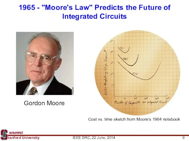
1965 - "Moore's Law" Predicts the Future of Integrated Circuits
Electronics Magazine
1965 - "Moore's Law" Predicts the Future of Integrated Circuits
Electronics Magazine
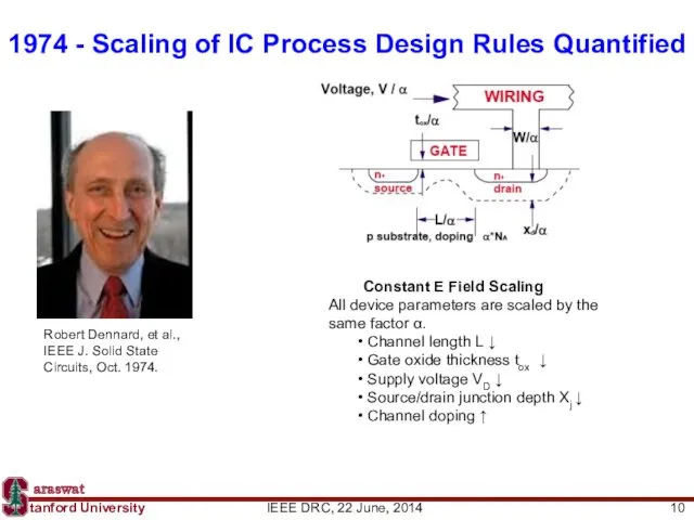
1974 - Scaling of IC Process Design Rules Quantified
Constant E Field
1974 - Scaling of IC Process Design Rules Quantified
Constant E Field
 Правила построения изображений
 Начертательная геометрия
 Восходящие и нисходящие прямые. Разбивка окружностей в перспективе. Построение перспектив методом сетки
 Пересечение поверхности плоскостью
 Резьбы. Резьбовые изделия и соединения
 Детали. Сборочный чертеж
 Оформление чертежа механически обработанной детали
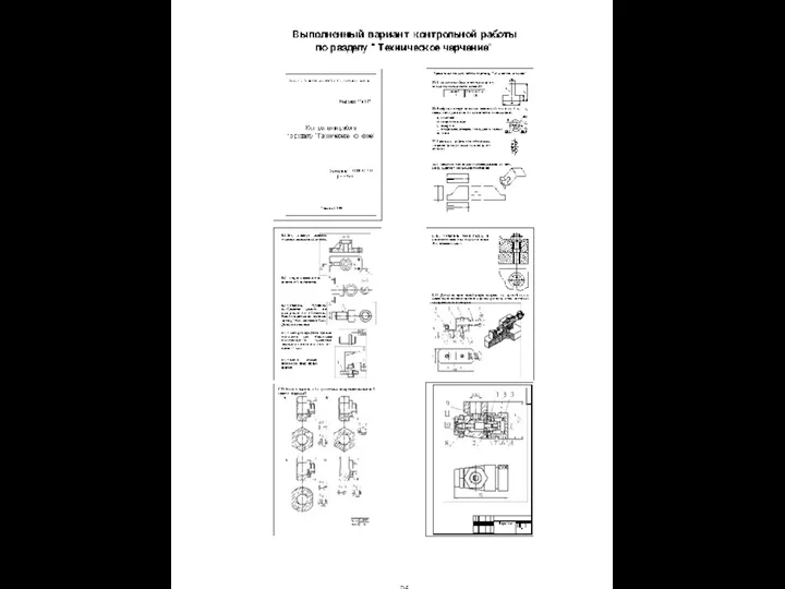 Техническое черчение. Контрольная работа
 Угловая перспектива
 Геометрические построения
 Резьба. Крепёжные изделия
 Черчение. Оформление чертежей. Построение третьего вида предмета по двум данным
 Изображения – виды, разрезы, сечения (лекция 3)
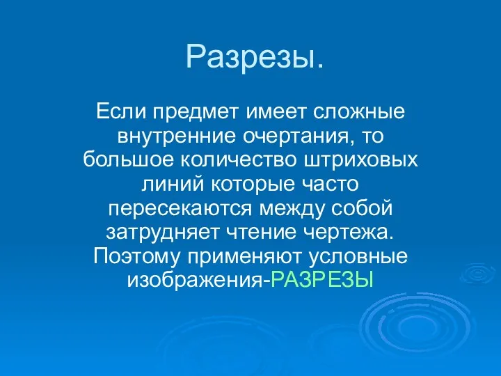 Разрезы. Обозначение фигуры сечения
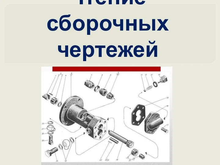 Чтение сборочных чертежей
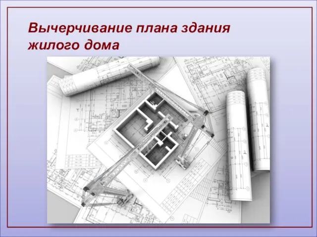 План здания (теория)
 Шрифты и надписи на картах
 Основи будівельного креслення
 Способы преобразования чертежа
 Рекомендации по выполнению контрольной работы по инженерной графике
 Інтенсифікація процесів очищення стічних вод методами кавітації
 Изображения: виды, разрезы, сечения
 Построение разрезов
 Резьбовое содинение
 Чертёж плоской детали, симметричной относительно одной плоскости симметрии. Алгоритм построения
 Нарезание наружной и внутренней резьбы
 Базовые ГОСТы
 Начертательная геометрия