- Types of Semiconductors

Содержание
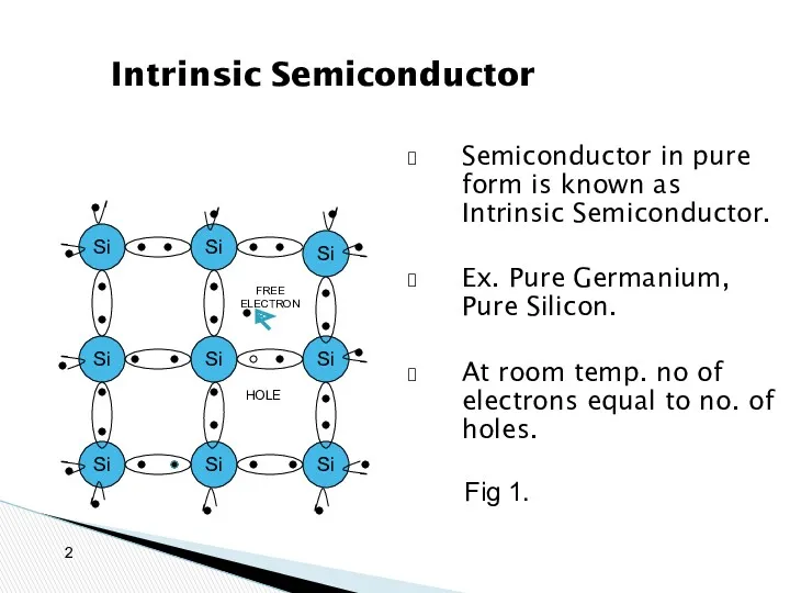
- 2. Intrinsic Semiconductor Semiconductor in pure form is known as Intrinsic Semiconductor. Ex. Pure Germanium, Pure Silicon.
- 3. Intrinsic semiconductor energy band diagram Fermi level lies in the middle Conduction Band Valence Band Energy
- 4. When we add an impurity to pure semiconductor to increase the charge carriers then it becomes
- 5. Comparison of semiconductors Intrinsic Semiconductor 1. It is in pure form. 2. Holes and electrons are
- 6. Comparison between n-type and p-type semiconductors N-type Pentavalent impurities are added. Majority carriers are electrons. Minority
- 7. When we add a pentavalent impurity to pure semiconductor we get n-type semiconductor. N-type Semiconductor As
- 8. When we add a Trivalent impurity to pure semiconductor we get p-type semiconductor. P-type Semiconductor Ga
- 9. In addition to this, some of the covalent bonds break due temperature and electron hole pairs
- 10. P and N type Semiconductors + + + + + + + + + + +
- 11. Comparison of semiconductors Intrinsic Semiconductor It is in pure form. Holes and electrons are equal. Fermi
- 12. Conduction is carried out by means of 1. Drift Process. 2. Diffusion Process. Conduction in Semiconductors
- 13. Drift process CB VB Electrons move from external circuit and in conduction band of a semiconductor.
- 14. Diffusion process X=a Moving of electrons from higher concentration gradient to lower concentration gradient is known
- 15. P and N type Semiconductors + + + + + + + + + + +
- 16. Formation of pn diode - - - - - - - - - - - +
- 17. Semiconductor diodes Fig. 1 Diode variants Visual - 1
- 19. Скачать презентацию
Intrinsic Semiconductor
Semiconductor in pure form is known as Intrinsic Semiconductor.
Ex. Pure
Intrinsic Semiconductor
Semiconductor in pure form is known as Intrinsic Semiconductor.
Ex. Pure
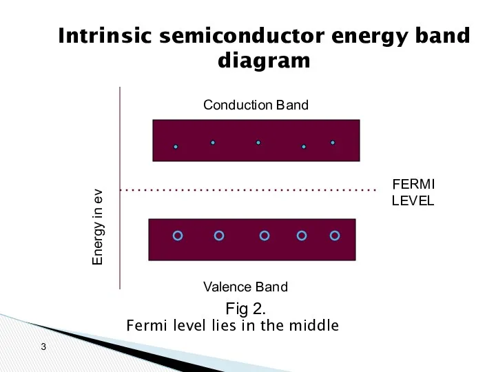
Intrinsic semiconductor energy band diagram
Fermi level lies in the middle
Conduction Band
Valence
Intrinsic semiconductor energy band diagram
Fermi level lies in the middle
Conduction Band
Valence
When we add an impurity to pure semiconductor to increase the
When we add an impurity to pure semiconductor to increase the
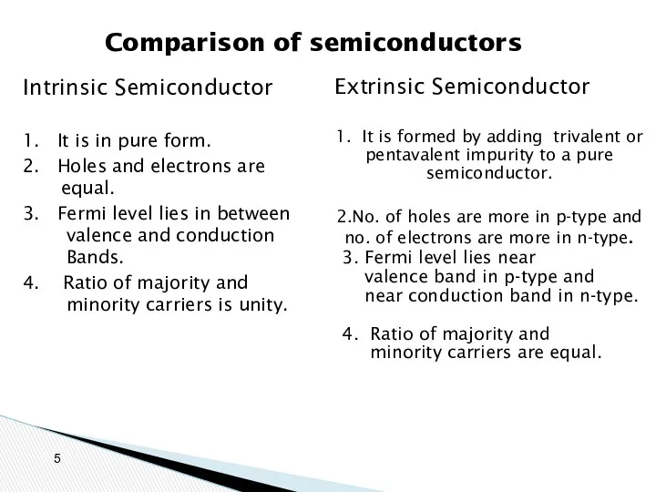
Comparison of semiconductors
Intrinsic Semiconductor
1. It is in pure form.
2. Holes and
Comparison of semiconductors
Intrinsic Semiconductor
1. It is in pure form.
2. Holes and
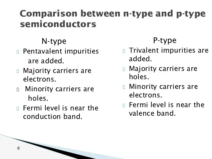
Comparison between n-type and p-type
semiconductors
N-type
Pentavalent impurities
are added.
Majority carriers are
Comparison between n-type and p-type
semiconductors
N-type
Pentavalent impurities
are added.
Majority carriers are
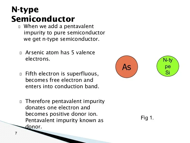
When we add a pentavalent impurity to pure semiconductor we get
When we add a pentavalent impurity to pure semiconductor we get
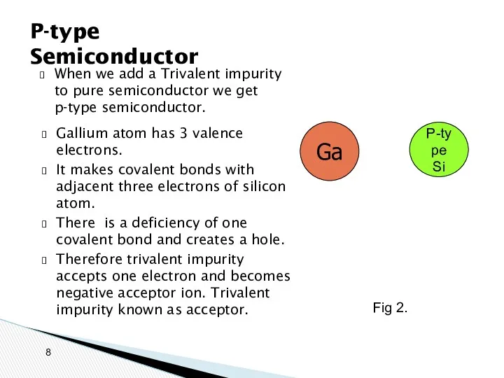
When we add a Trivalent impurity to pure semiconductor we get
When we add a Trivalent impurity to pure semiconductor we get
In addition to this, some of the covalent bonds break due
In addition to this, some of the covalent bonds break due
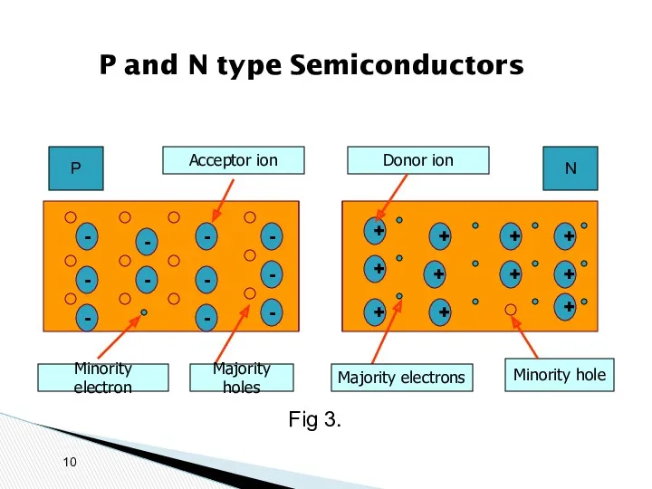
P and N type Semiconductors
+
+
+
+
+
+
+
+
+
+
+
N
-
-
-
-
-
-
-
-
-
-
-
P
Acceptor ion
Donor ion
Minority electron
Minority hole
Majority holes
Majority electrons
Fig
P and N type Semiconductors
+
+
+
+
+
+
+
+
+
+
+
N
-
-
-
-
-
-
-
-
-
-
-
P
Acceptor ion
Donor ion
Minority electron
Minority hole
Majority holes
Majority electrons
Fig
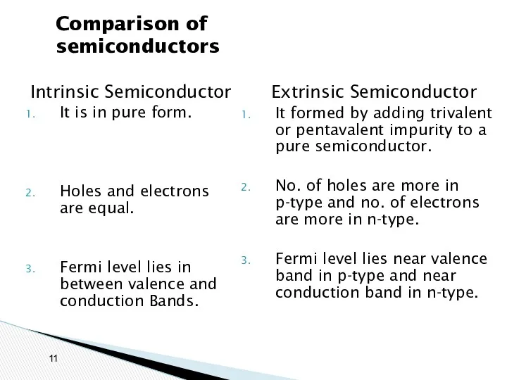
Comparison of semiconductors
Intrinsic Semiconductor
It is in pure form.
Holes and electrons are
Comparison of semiconductors
Intrinsic Semiconductor
It is in pure form.
Holes and electrons are
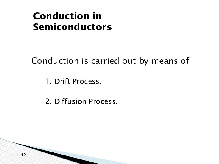
Conduction is carried out by means of
1. Drift Process.
2. Diffusion
Conduction is carried out by means of
1. Drift Process.
2. Diffusion
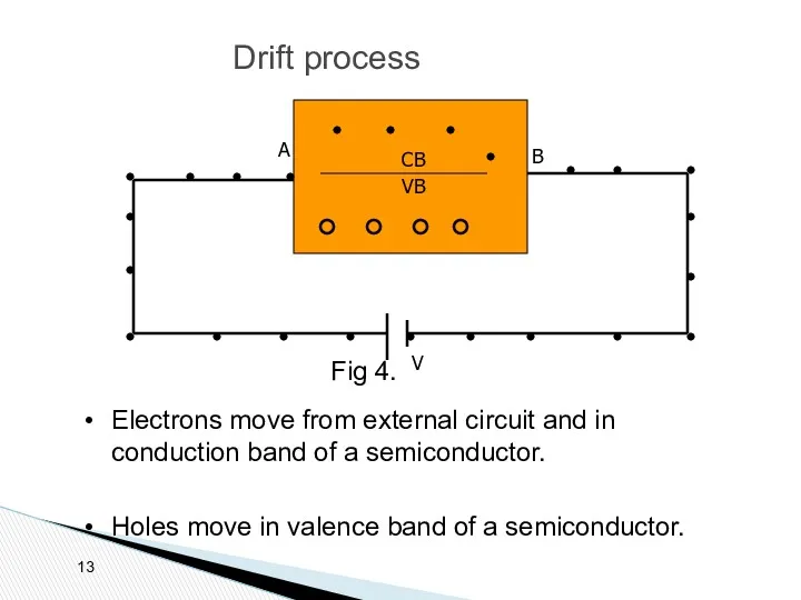
Drift process
CB
VB
Electrons move from external circuit and in conduction band of
Drift process
CB
VB
Electrons move from external circuit and in conduction band of
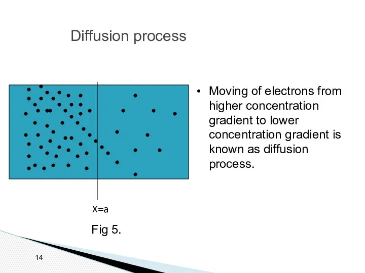
Diffusion process
X=a
Moving of electrons from higher concentration gradient to lower concentration
Diffusion process
X=a
Moving of electrons from higher concentration gradient to lower concentration
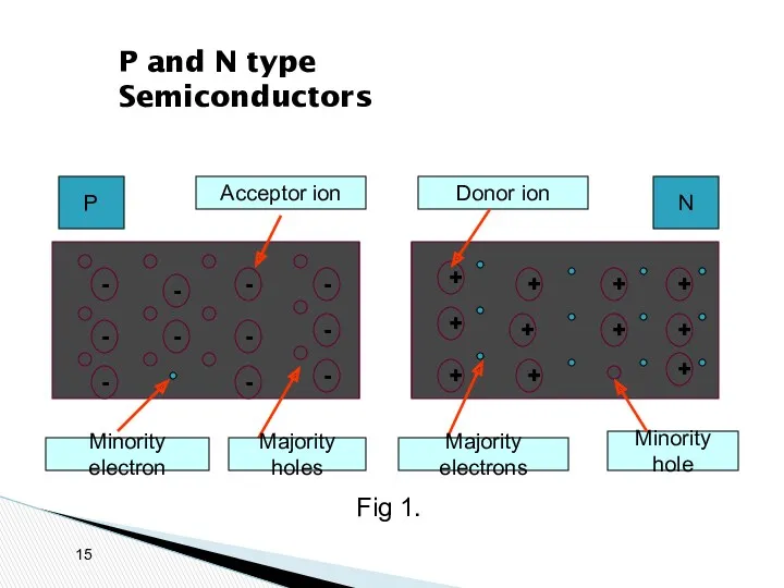
P and N type Semiconductors
+
+
+
+
+
+
+
+
+
+
+
N
-
-
-
-
-
-
-
-
-
-
-
P
Acceptor ion
Donor ion
Minority electron
Minority hole
Majority holes
Majority electrons
Fig
P and N type Semiconductors
+
+
+
+
+
+
+
+
+
+
+
N
-
-
-
-
-
-
-
-
-
-
-
P
Acceptor ion
Donor ion
Minority electron
Minority hole
Majority holes
Majority electrons
Fig
Formation of pn diode
-
-
-
-
-
-
-
-
-
-
-
+
+
+
+
+
+
+
+
+
+
+
Depletion Region
Vb
P
N
Potential barrier
Fig 2.
Formation of pn diode
-
-
-
-
-
-
-
-
-
-
-
+
+
+
+
+
+
+
+
+
+
+
Depletion Region
Vb
P
N
Potential barrier
Fig 2.
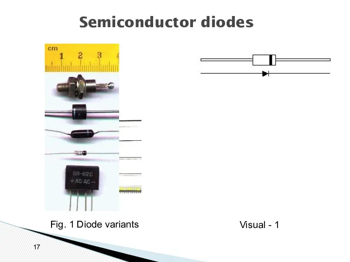
Semiconductor diodes
Fig. 1 Diode variants
Visual - 1
Semiconductor diodes
Fig. 1 Diode variants
Visual - 1
 Взаимодействие заряженных тел. Закон Кулона. Закон сохранения электрического заряда. Электрическое поле
 Физические основы механики. Элементы кинематики
 Роль испарения и конденсации в природе, в жизни человека и животных
 Свободные затухающие колебания. Дифференциальное уравнение затухающих колебаний
 урок по физике Магнитное поле
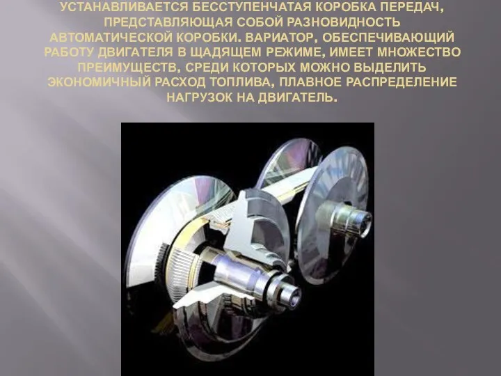 Бесступенчатая коробка передач
 Архимед (287 - 212 до н.э.)
 Тербелістер мен толқындар
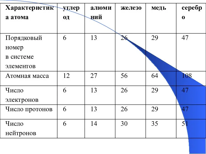 презентация физика 8
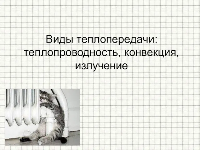 Виды теплопередачи теплопроводность, конвекция, излучение
 Урок Обобщение материала по теме Силы в природе. 7 класс.
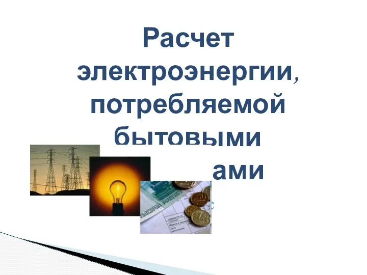 Электрические явления. Расчет электроэнергии, потребляемой бытовыми приборами. (8 класс)
 Закон Ома для участка цепи
 Фізичні та хімічні явища. (7 клас)
 Улаштування та ТО рульового керування
 Физика в спорте
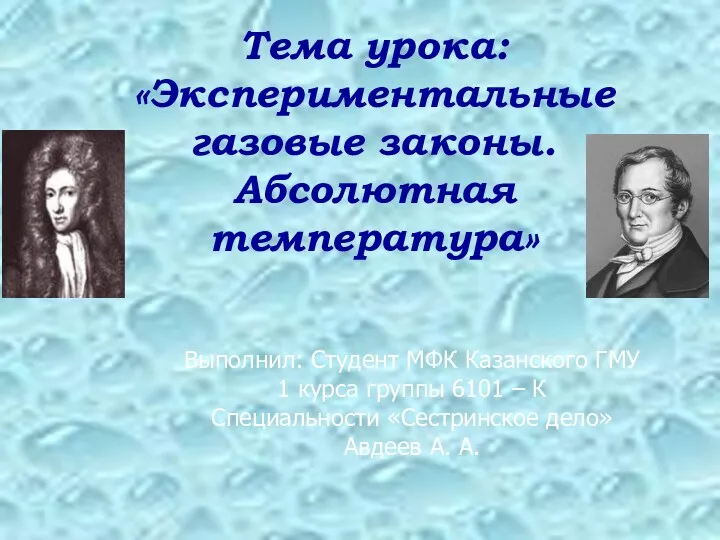 Экспериментальные газовые законы. Абсолютная температура
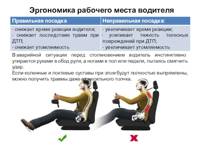 Рабочее место водителя
 Взаимодействие света с веществом. Дисперсия света. Нормальная и аномальная дисперсия. Классическая теория дисперсии
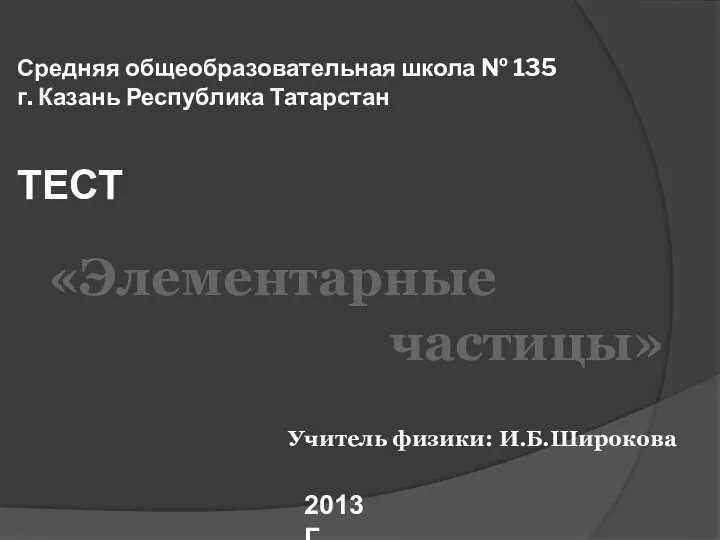 Тест по теме Элементарные частицы 11 класс
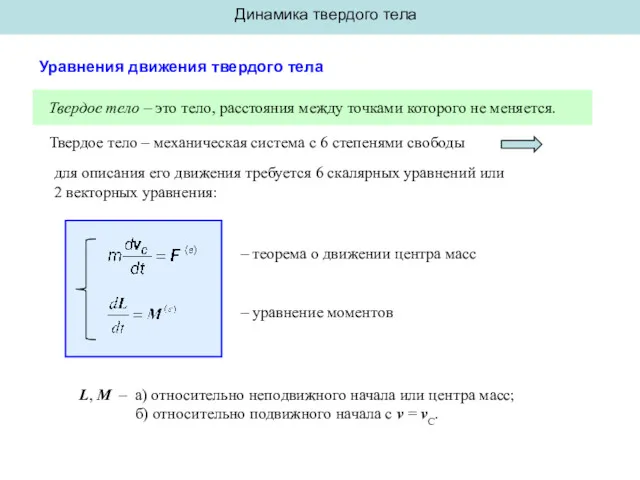 Динамика твердого тела. Уравнения движения твердого тела
 презентация к уроку Диффузия вещества. Золото этрусков.
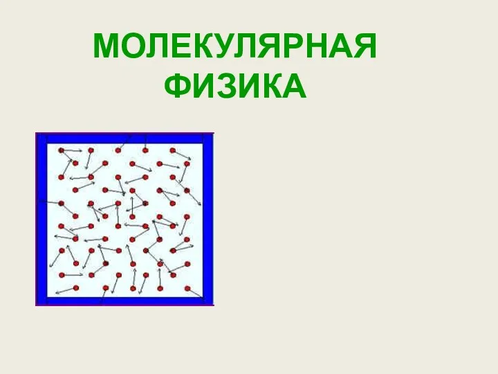 Законы и формулы молекулярной физики
 Модель урока по теме Тела и их взаимодействие. Инерциальное движение.
 Расчёт пути и времени движения (физика,7 класс)
 Сопротивление материалов. Введение. Основные понятия
 Проектирование и конструирование. Механические передачи
 Электромагнитная совместимость