- Bus-modular structure of the PC Von Neumann Architecture

Содержание
- 2. Learning objectives show understanding of how data are transferred between various components of the computer system
- 3. Von Neumann Architecture
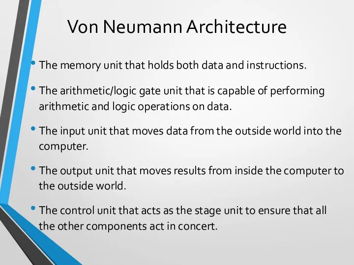
- 4. Von Neumann Architecture The memory unit that holds both data and instructions. The arithmetic/logic gate unit
- 5. RAM - Random Access Memory can be read from and written to. Data is cleared when
- 6. Input/Output Units An Input Unit is a device through which data and programs from the outside
- 7. Arithmetic/Logic Unit The ALU is a fundamental building block in the central processing unit (CPU) of
- 8. Control unit The control unit sits inside the CPU and coordinates the input and output devices
- 9. Bus-modular structure of the PC
- 10. LMC CPU Structure Visible registers shown in red Accumulators Data for calculation Data Word to/from memory
- 11. Registers Registers - a small amount of fast storage which is part of the processor Program
- 12. Processor clock A timing device connected to the processor that synchronises when the fetch, decode execute
- 13. System Bus A Bus is a connection between different devices. This connection will normally consist of
- 14. Address Bus A single-directional bus that carries address signals from the CPU to Main Memory and
- 15. Data bus A bi-directional bus, typically consisting of 32 wires, used to transport data and instructions
- 16. Control bus A bi-directional bus, typically consisting of more than 16 wires, used to transport control
- 17. Clock Processor Main memory keyboard controller VDU controller Disk controller Data bus (or Control bus) Control
- 18. Fetch-Execute Each instruction cycle consists on two subcycles Fetch cycle Load the next instruction (Opcode +
- 19. Fetch Instruction Program counter to address register Read memory at address Memory data to ‘Data’ ‘Data’
- 20. Execute Instruction Decode instruction Address from instruction to ‘address register’ Access memory Data from memory to
- 21. The Fetch-Execute Cycle The process cycle includes four steps: Fetch the next instruction, Decode the instruction
- 22. Fetch the Next Instruction The PC increments one by one to point to the next instruction
- 23. Decode the Instruction To execute the instruction in the instruction register, the control unit has to
- 24. Get Data If Needed The instruction to be executed may potentially require additional memory accesses to
- 25. Execute the Instruction Once an instruction has been decoded and any operands (data) fetched, the control
- 26. Fetch The Program Counter (PC) contains the address of the next instruction to be fetched. The
- 27. Процессор выставляет число, хранящееся в регистре счётчика команд, на шину адреса, и отдаёт памяти команду чтения;
- 29. Скачать презентацию
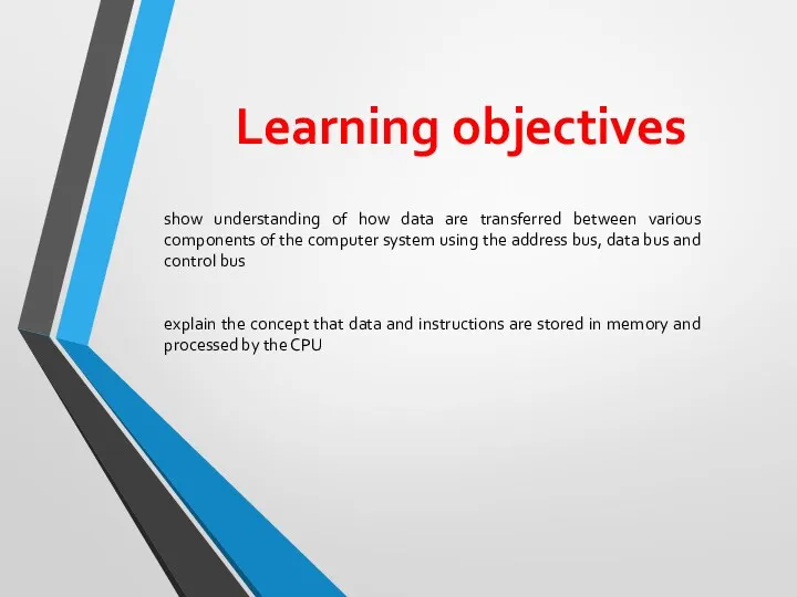
Learning objectives
show understanding of how data are transferred between various components
Learning objectives
show understanding of how data are transferred between various components
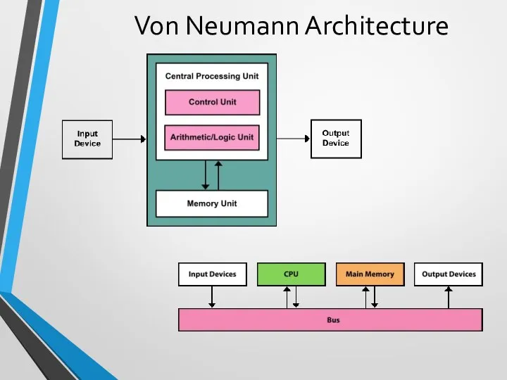
Von Neumann Architecture
Von Neumann Architecture
Von Neumann Architecture
The memory unit that holds both data and instructions.
The
Von Neumann Architecture
The memory unit that holds both data and instructions.
The
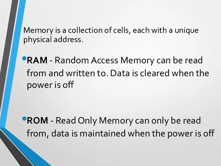
RAM - Random Access Memory can be read from and written to.
RAM - Random Access Memory can be read from and written to.
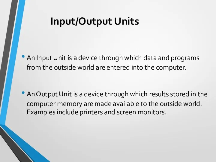
Input/Output Units
An Input Unit is a device through which data and
Input/Output Units
An Input Unit is a device through which data and
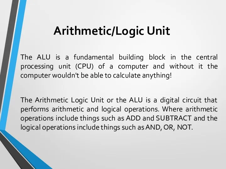
Arithmetic/Logic Unit
The ALU is a fundamental building block in the central
Arithmetic/Logic Unit
The ALU is a fundamental building block in the central
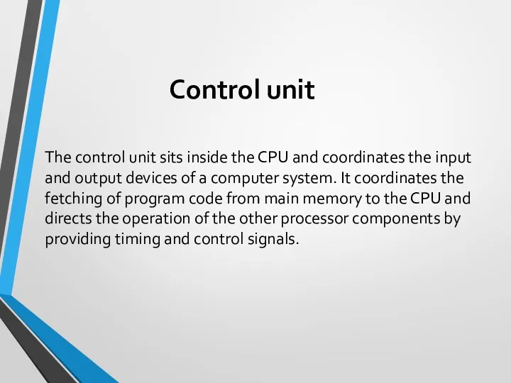
Control unit
The control unit sits inside the CPU and coordinates the
Control unit
The control unit sits inside the CPU and coordinates the
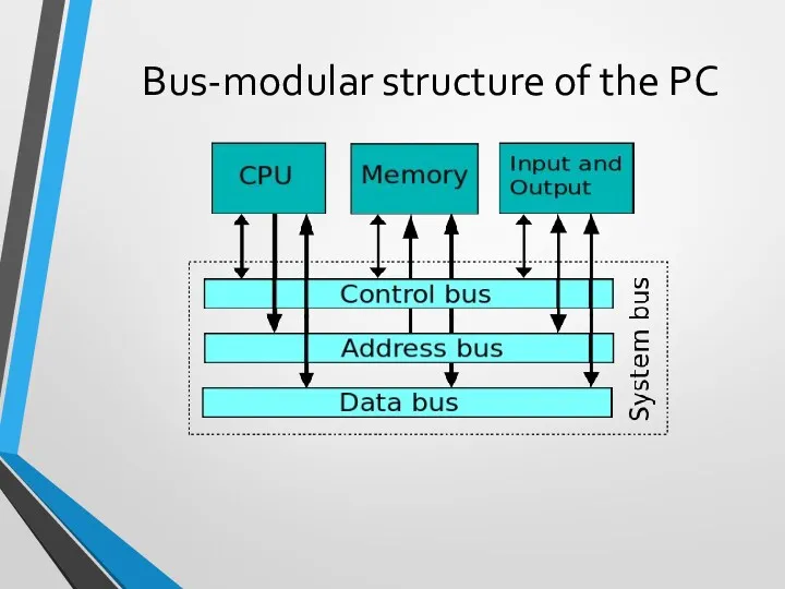
Bus-modular structure of the PC
Bus-modular structure of the PC
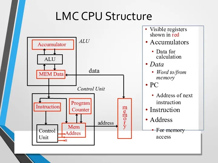
LMC CPU Structure
Visible registers shown in red
Accumulators
Data for calculation
Data
Word to/from memory
PC
Address
LMC CPU Structure
Visible registers shown in red
Accumulators
Data for calculation
Data
Word to/from memory
PC
Address
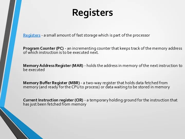
Registers
Registers - a small amount of fast storage which is part of
Registers
Registers - a small amount of fast storage which is part of
Processor clock
A timing device connected to the processor that synchronises when
Processor clock
A timing device connected to the processor that synchronises when
System Bus
A Bus is a connection between different devices. This connection
System Bus
A Bus is a connection between different devices. This connection
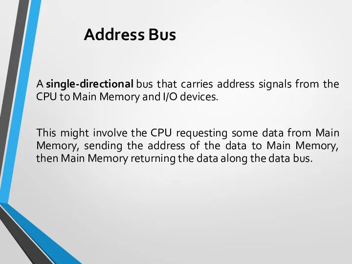
Address Bus
A single-directional bus that carries address signals from the CPU to Main
Address Bus
A single-directional bus that carries address signals from the CPU to Main
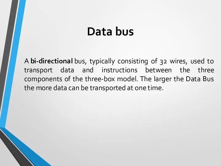
Data bus
A bi-directional bus, typically consisting of 32 wires, used to transport data
Data bus
A bi-directional bus, typically consisting of 32 wires, used to transport data
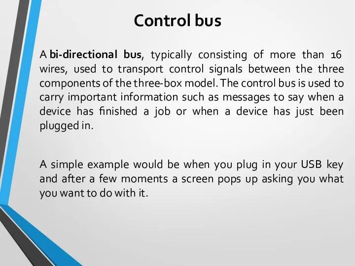
Control bus
A bi-directional bus, typically consisting of more than 16 wires, used
Control bus
A bi-directional bus, typically consisting of more than 16 wires, used
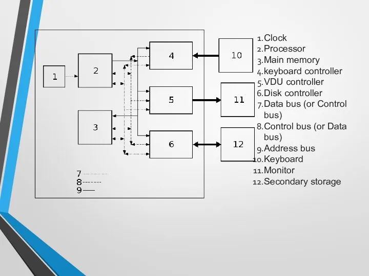
Clock
Processor
Main memory
keyboard controller
VDU controller
Disk controller
Data bus (or Control bus)
Control bus (or
Clock
Processor
Main memory
keyboard controller
VDU controller
Disk controller
Data bus (or Control bus)
Control bus (or
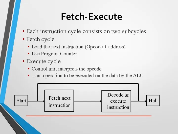
Fetch-Execute
Each instruction cycle consists on two subcycles
Fetch cycle
Load the next instruction
Fetch-Execute
Each instruction cycle consists on two subcycles
Fetch cycle
Load the next instruction
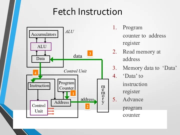
Fetch Instruction
Program
counter to address register
Read memory at address
Memory data to ‘Data’
‘Data’
Fetch Instruction
Program
counter to address register
Read memory at address
Memory data to ‘Data’
‘Data’
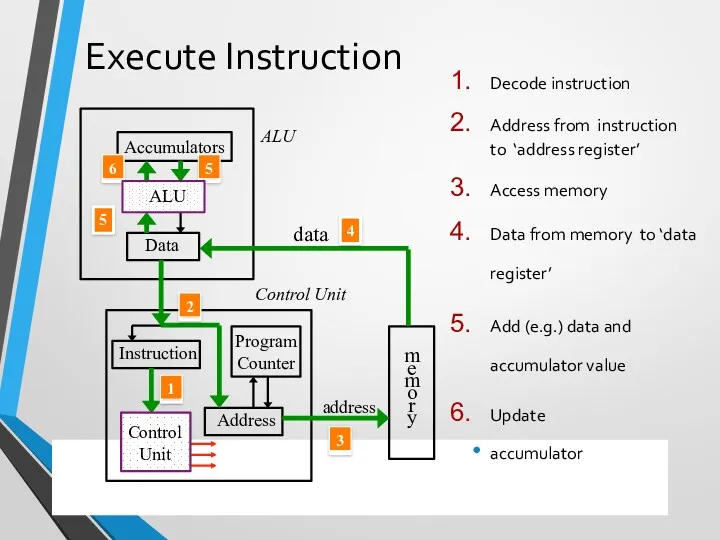
Execute Instruction
Decode instruction
Address from instruction to ‘address register’
Access memory
Data from memory
Execute Instruction
Decode instruction
Address from instruction to ‘address register’
Access memory
Data from memory
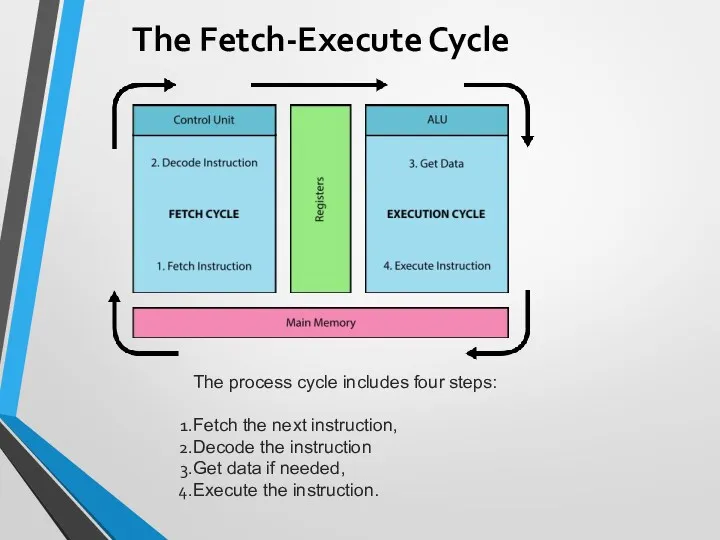
The Fetch-Execute Cycle
The process cycle includes four steps:
Fetch the next instruction,
Decode
The Fetch-Execute Cycle
The process cycle includes four steps:
Fetch the next instruction,
Decode
Fetch the Next Instruction
The PC increments one by one to point to the
Fetch the Next Instruction
The PC increments one by one to point to the
Decode the Instruction
To execute the instruction in the instruction register, the
Decode the Instruction
To execute the instruction in the instruction register, the
Get Data If Needed
The instruction to be executed may potentially require
Get Data If Needed
The instruction to be executed may potentially require
Execute the Instruction
Once an instruction has been decoded and any operands
Execute the Instruction
Once an instruction has been decoded and any operands
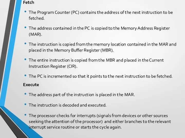
Fetch
The Program Counter (PC) contains the address of the next
Fetch
The Program Counter (PC) contains the address of the next
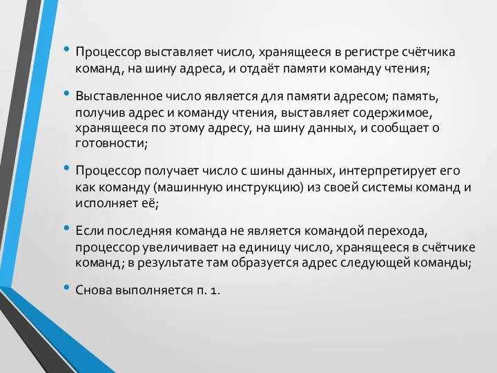
Процессор выставляет число, хранящееся в регистре счётчика команд, на шину адреса,
Процессор выставляет число, хранящееся в регистре счётчика команд, на шину адреса,
 Сравнительный анализ дизайна сайтов
 Формирование метапредметных компетенций учащихся на уроках информатики
 Состав и структура АИС
 Угрозы информации
 Алгоритм шифрования RSA. Лекция 10
 Архитектура персонального компьютера
 Принципы машинного обучения, нейронных сетей
 Информация. Её виды и свойства
 Writing research articles. IMRD. Format. Overview
 слайд-шоу к занятию по робототехнике
 Программирование на Python. Урок 10. Анимация и передвижение
 Облачные технологии
 Исчисления и модели данных
 Клавиатура
 Модель OSI. 7 уровней
 Social Media is changing the English language
 Системы автоматизированного проектирования (САПР)
 Продвижение библиотеки в социальных сетях
 Умный дом. Преимущества и возможности
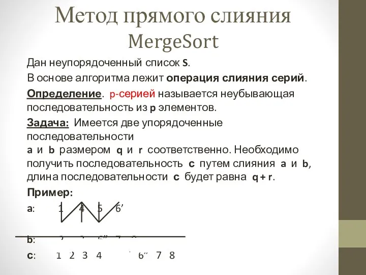 Метод прямого слияния MergeSort
 Application Server 2017
 Case Study for Saas Based Portal for HRMS SAP Integration
 Модуль управления движением автомобиля для системы оценки профессиональной пригодности водителей автотранспорта
 Алгоритм и алгоритмические структуры, структурное программирование
 Основні технічні та управлінські проблеми супроводження програмного забезпечення
 Интеллектуальные информационные системы (ИИС). Лекция 4. Семантические сети
 Презентация к уроку Файлы и файловая система
 Принципы автоматизированного управления автономной системой отопления