- Selecting Gate Driver Tutorial

Содержание
- 2. Selection and/or Design-in Criteria How many inputs/outputs required from the Gate Driver ? Required Voltage rating
- 3. How many inputs/output are provided for/by the Gate driver? For the inputs, It depends on the
- 4. How much drive current is required? Information about the required gate charge to raise the gate
- 5. Special functions Some applications need special functions like inbuilt and/or adjustable dead time, enable option, shoot
- 6. The capacitance of the bootstrap capacitor should be high enough to provide the charge required by
- 7. Bootstrap Diode selection Some of the DGDXXX series gate drivers come with an internal bootstrap diode
- 8. Gate Resistor Selection A typical gate drive current control circuit is shown here. By adjusting the
- 9. Switch Node Noise Management Switch node shown in the figure as VS, is the noisiest node
- 11. Скачать презентацию

Selection and/or Design-in Criteria
How many inputs/outputs required from the Gate Driver
Selection and/or Design-in Criteria
How many inputs/outputs required from the Gate Driver

How many inputs/output are provided for/by the Gate driver?
For the inputs,
How many inputs/output are provided for/by the Gate driver?
For the inputs,

How much drive current is required?
Information about the required gate
How much drive current is required?
Information about the required gate

Special functions
Some applications need special functions like inbuilt and/or adjustable dead
Special functions
Some applications need special functions like inbuilt and/or adjustable dead

The capacitance of the bootstrap capacitor should be high enough to
The capacitance of the bootstrap capacitor should be high enough to

Bootstrap Diode selection
Some of the DGDXXX series gate drivers come with
Bootstrap Diode selection
Some of the DGDXXX series gate drivers come with

Gate Resistor Selection
A typical gate drive current control circuit is shown
Gate Resistor Selection
A typical gate drive current control circuit is shown

Switch Node Noise Management
Switch node shown in the figure as VS,
Switch Node Noise Management
Switch node shown in the figure as VS,
 Разновидности .NET
 16 сарамандық жұмыс
 Контент - план
 3D-графика
 Поняття комп’ютерного вірусу
 Программное обеспечение для конфигурации материнской платы (DMI). Новый DMIFIT Tool на базе UEFI
 Возможности сетевых технологий для разработки электронного пособия Основы проектирования баз данных
 Интеллектуальная игра для обучающихся 8-10 лет
 Битва розумів. Позакласний захід з інформатики для 10-11 класу
 Безопасность в Интернете
 Состав и назначение интегрированных САПР. Лекция 5
 Робота зі ЗМІ
 Массивы
 Интерфейс Adobe Photoshop
 Технології колективної комунікації
 Спиральная модель проектирования
 Курсовая работа по дисциплине: системное программирование. Диспетчер файлов
 Наследование. Базовые понятия и примеры (лекция 8)
 Отображение информации в Ecdis
 20230928_2-5_sistemy_schisleniya
 Разветвляющиеся алгоритмы на языке Паскаль
 Module 1: Introducing Siebel Applications
 презентация по информатике Кодирование числовой информации
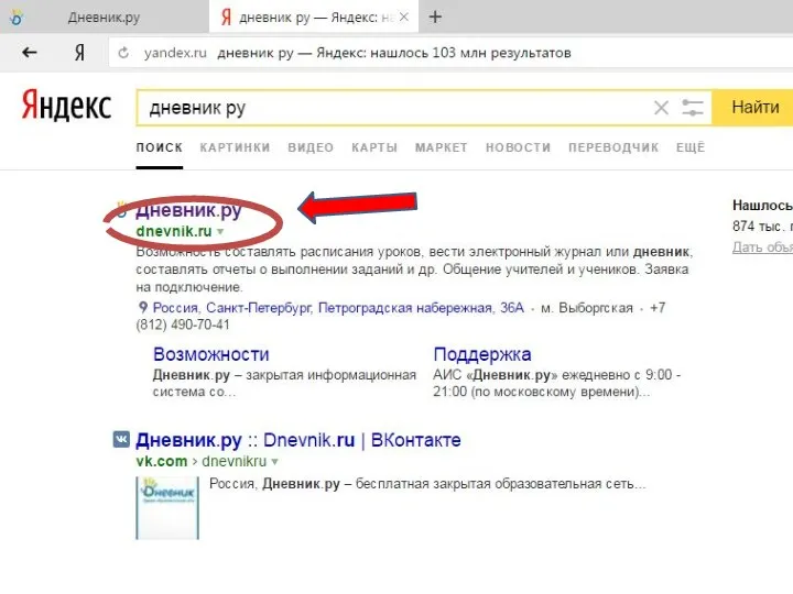 Электронный дневник
 Компьютерная графика
 Що таке Angular
 Система комп’ютерного моделювання процесів життєдіяльності органів і систем організму СКІФ
 Урок в 8 классе по теме Компьютерные презентации