- BP560X System Application Notes

Содержание
- 2. www.bpsemi.com Contents Patent Effect Typical Applications / Overview Examples of Design Considerations of Design
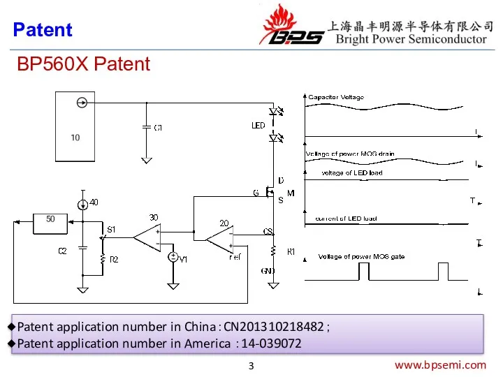
- 3. www.bpsemi.com Patent application number in China:CN201310218482; Patent application number in America :14-039072 BP560X Patent Patent
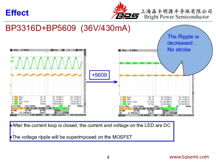
- 4. www.bpsemi.com Io Vo +5609 Effect BP3316D+BP5609 (36V/430mA) The Ripple is decreased , No strobe After the
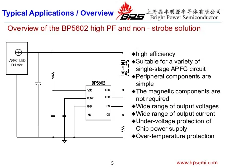
- 5. www.bpsemi.com high efficiency Suitable for a variety of single-stage APFC circuit Peripheral components are simple The
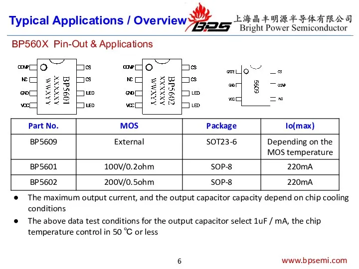
- 6. www.bpsemi.com BP560X Pin-Out & Applications Typical Applications / Overview The maximum output current, and the output
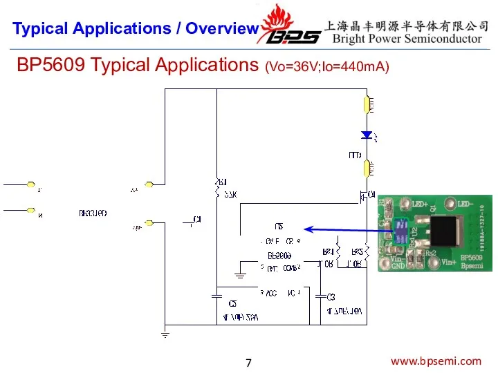
- 7. www.bpsemi.com BP5609 Typical Applications (Vo=36V;Io=440mA) Typical Applications / Overview
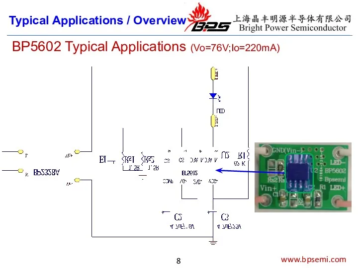
- 8. www.bpsemi.com BP5602 Typical Applications (Vo=76V;Io=220mA) Typical Applications / Overview
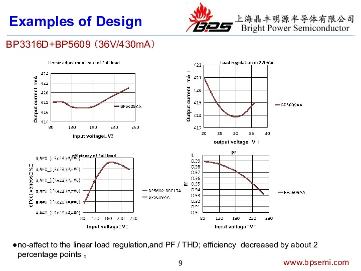
- 9. Examples of Design BP3316D+BP5609 (36V/430mA) no-affect to the linear load regulation,and PF / THD; efficiency decreased
- 10. Examples of Design www.bpsemi.com Selection of pre-output capacitor According to the output current, it is recommended
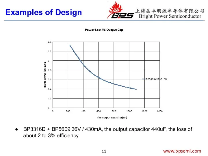
- 11. Examples of Design www.bpsemi.com BP3316D + BP5609 36V / 430mA, the output capacitor 440uF, the loss
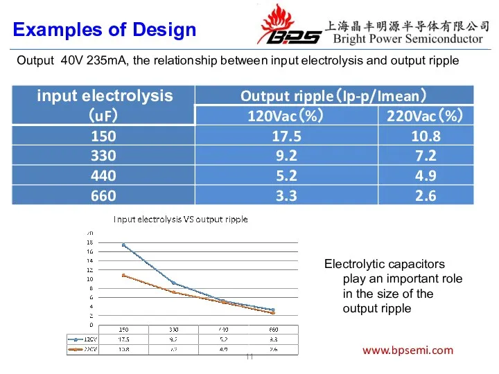
- 12. 11 www.bpsemi.com Examples of Design Output 40V 235mA, the relationship between input electrolysis and output ripple
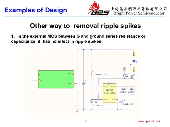
- 13. 13 www.bpsemi.com 1、 In the external MOS between G and ground series resistance or capacitance, it
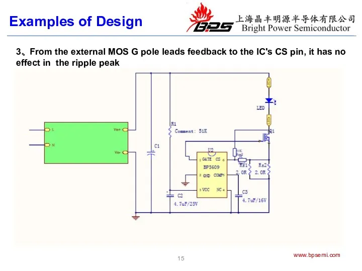
- 14. 15 www.bpsemi.com 3、 From the external MOS G pole leads feedback to the IC's CS pin,
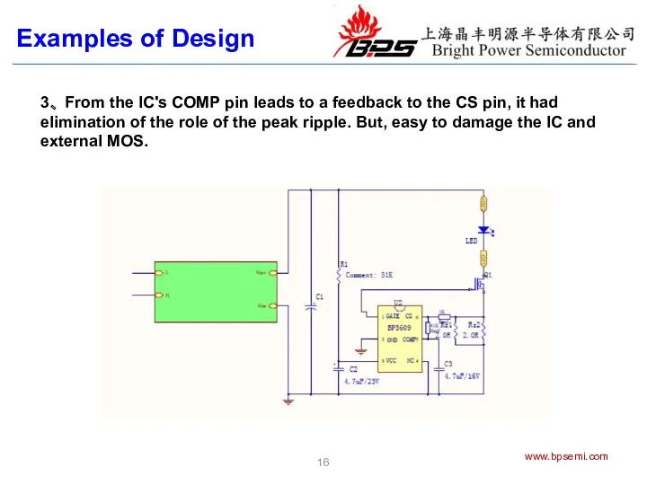
- 15. 16 www.bpsemi.com 3、 From the IC's COMP pin leads to a feedback to the CS pin,
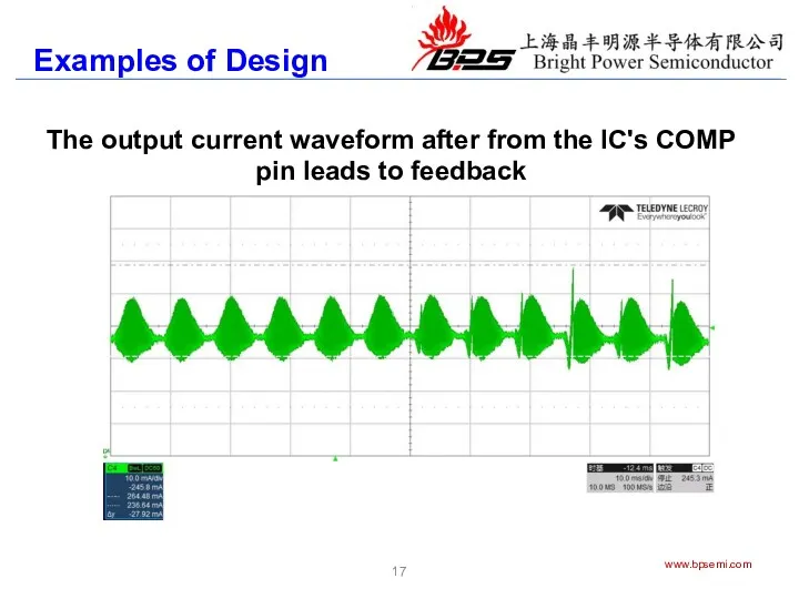
- 16. 17 www.bpsemi.com Examples of Design The output current waveform after from the IC's COMP pin leads
- 17. Examples of Design www.bpsemi.com Pre-APFC'S capacitor parameters requirements Pre-APFC'S COMP capacitor capacitance should not be greater
- 18. www.bpsemi.com Considerations of Design Start resistor and VCC capacitor selection The starting resistor is selected according
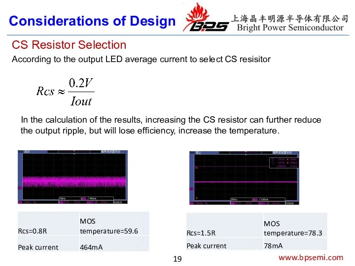
- 19. www.bpsemi.com Considerations of Design CS Resistor Selection According to the output LED average current to select
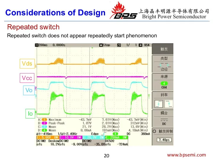
- 20. www.bpsemi.com Considerations of Design Repeated switch Repeated switch does not appear repeatedly start phenomenon Vo Vcc
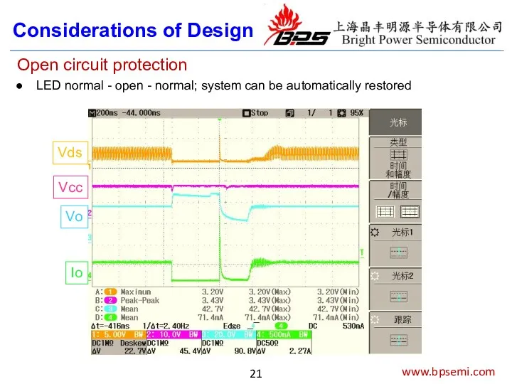
- 21. www.bpsemi.com Considerations of Design Open circuit protection LED normal - open - normal; system can be
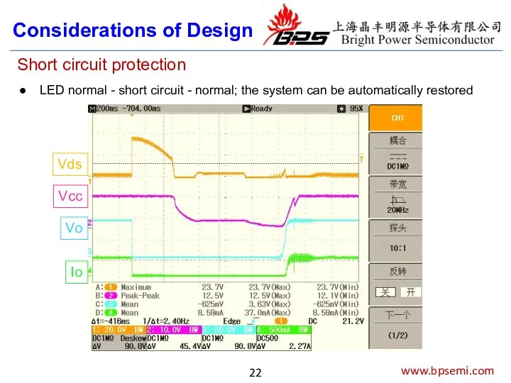
- 22. www.bpsemi.com Considerations of Design Short circuit protection LED normal - short circuit - normal; the system
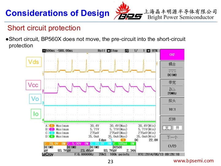
- 23. www.bpsemi.com Considerations of Design Short circuit protection Short circuit, BP560X does not move, the pre-circuit into
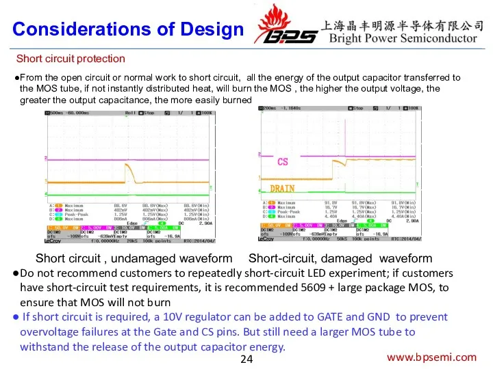
- 24. www.bpsemi.com Considerations of Design Short circuit protection From the open circuit or normal work to short
- 26. Скачать презентацию
www.bpsemi.com
Contents
Patent
Effect
Typical Applications / Overview
Examples of Design
Considerations of Design
www.bpsemi.com
Contents
Patent
Effect
Typical Applications / Overview
Examples of Design
Considerations of Design
www.bpsemi.com
Patent application number in China:CN201310218482;
Patent application number in America :14-039072
BP560X
www.bpsemi.com
Patent application number in China:CN201310218482;
Patent application number in America :14-039072
BP560X
www.bpsemi.com
Io
Vo
+5609
Effect
BP3316D+BP5609 (36V/430mA)
The Ripple is decreased , No strobe
After the current loop
www.bpsemi.com
Io
Vo
+5609
Effect
BP3316D+BP5609 (36V/430mA)
The Ripple is decreased , No strobe
After the current loop
www.bpsemi.com
high efficiency
Suitable for a variety of single-stage APFC circuit
Peripheral components are
www.bpsemi.com
high efficiency
Suitable for a variety of single-stage APFC circuit
Peripheral components are
www.bpsemi.com
BP560X Pin-Out & Applications
Typical Applications / Overview
The maximum output current, and
www.bpsemi.com
BP560X Pin-Out & Applications
Typical Applications / Overview
The maximum output current, and
www.bpsemi.com
BP5609 Typical Applications (Vo=36V;Io=440mA)
Typical Applications / Overview
www.bpsemi.com
BP5609 Typical Applications (Vo=36V;Io=440mA)
Typical Applications / Overview
www.bpsemi.com
BP5602 Typical Applications (Vo=76V;Io=220mA)
Typical Applications / Overview
www.bpsemi.com
BP5602 Typical Applications (Vo=76V;Io=220mA)
Typical Applications / Overview
Examples of Design
BP3316D+BP5609 (36V/430mA)
no-affect to the linear load regulation,and PF /
Examples of Design
BP3316D+BP5609 (36V/430mA)
no-affect to the linear load regulation,and PF /
Examples of Design
www.bpsemi.com
Selection of pre-output capacitor
According to the output current, it
Examples of Design
www.bpsemi.com
Selection of pre-output capacitor
According to the output current, it
Examples of Design
www.bpsemi.com
BP3316D + BP5609 36V / 430mA, the output capacitor
Examples of Design
www.bpsemi.com
BP3316D + BP5609 36V / 430mA, the output capacitor
11
www.bpsemi.com
Examples of Design
Output 40V 235mA, the relationship between input electrolysis and
11
www.bpsemi.com
Examples of Design
Output 40V 235mA, the relationship between input electrolysis and
13
www.bpsemi.com
1、 In the external MOS between G and ground series resistance
13
www.bpsemi.com
1、 In the external MOS between G and ground series resistance
15
www.bpsemi.com
3、 From the external MOS G pole leads feedback to the
15
www.bpsemi.com
3、 From the external MOS G pole leads feedback to the
16
www.bpsemi.com
3、 From the IC's COMP pin leads to a feedback to
16
www.bpsemi.com
3、 From the IC's COMP pin leads to a feedback to
17
www.bpsemi.com
Examples of Design
The output current waveform after from the IC's COMP
17
www.bpsemi.com
Examples of Design
The output current waveform after from the IC's COMP
Examples of Design
www.bpsemi.com
Pre-APFC'S capacitor parameters requirements
Pre-APFC'S COMP capacitor capacitance should not
Examples of Design
www.bpsemi.com
Pre-APFC'S capacitor parameters requirements
Pre-APFC'S COMP capacitor capacitance should not
www.bpsemi.com
Considerations of Design
Start resistor and VCC capacitor selection
The starting resistor is
www.bpsemi.com
Considerations of Design
Start resistor and VCC capacitor selection
The starting resistor is
www.bpsemi.com
Considerations of Design
CS Resistor Selection
According to the output LED average
www.bpsemi.com
Considerations of Design
CS Resistor Selection
According to the output LED average
www.bpsemi.com
Considerations of Design
Repeated switch
Repeated switch does not appear repeatedly start phenomenon
Vo
Vcc
Io
Vds
www.bpsemi.com
Considerations of Design
Repeated switch
Repeated switch does not appear repeatedly start phenomenon
Vo
Vcc
Io
Vds
www.bpsemi.com
Considerations of Design
Open circuit protection
LED normal - open - normal; system
www.bpsemi.com
Considerations of Design
Open circuit protection
LED normal - open - normal; system
www.bpsemi.com
Considerations of Design
Short circuit protection
LED normal - short circuit - normal;
www.bpsemi.com
Considerations of Design
Short circuit protection
LED normal - short circuit - normal;
www.bpsemi.com
Considerations of Design
Short circuit protection
Short circuit, BP560X does not move, the
www.bpsemi.com
Considerations of Design
Short circuit protection
Short circuit, BP560X does not move, the
www.bpsemi.com
Considerations of Design
Short circuit protection
From the open circuit or normal work
www.bpsemi.com
Considerations of Design
Short circuit protection
From the open circuit or normal work
 Разработка эффективного ивент-мероприятия на примере компании Гарнье
 Триггеры. RS - триггер,
 Пасха. Символы Пасхи
 Понятие, сущность и основные функции менеджмента
 Itogovy_keys_Poklyovochka (2)
 Компания РЖД Логистика
 Текстильная промышленность
 ИИП на конкурс Настя 06.04
 Prezentatsia_bez_nazvania 1
 Системний блок комп'ютера
 Транспортная инфраструктура
 Презентация Огород на подоконнике
 Презентация Экологическая игра
 Семья. Качества счастливой семьи
 Салық – мемлекеттік бюджетке заңды және жеке тұлғалардан белгілі бір мөлшерде түсетін міндетті
 Речевое поведение педагога
 Обыкновенные дроби. (5 класс)
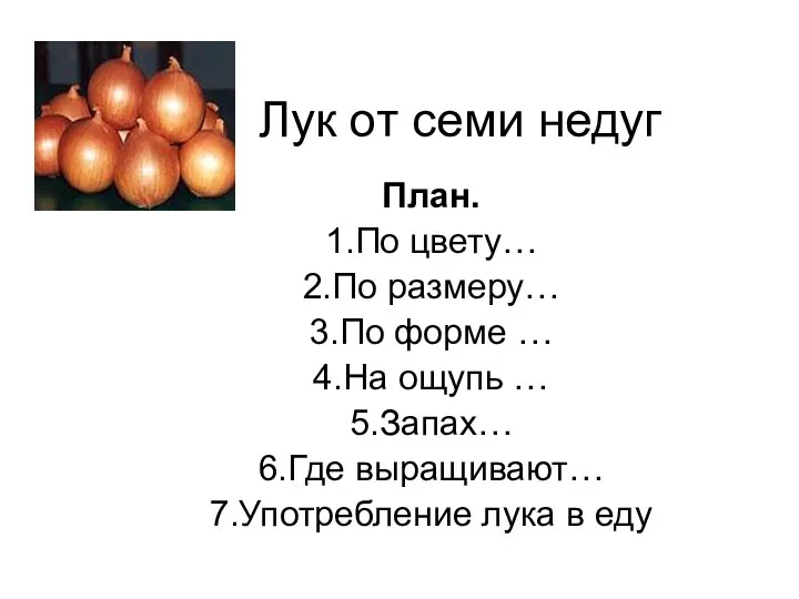 презентация Лук от семи недуг
 Правописание гласных в падежных окончаниях имен прилагательных
 Оценка готовности детей к школе
 Путешествие по континенту Химия
 Спрос и предложение
 Моя публикация. Разработка урока по химии 8 класс для детей ОВЗ
 Дидактическая игра Третий - лишний (зимующие и перелётные птицы)
 Презентации по геологии
 Инструкция по работе с ресурсами ИЗО
 МАИ – ведущий аэрокосмический вуз России
 Знакомство с сетевой академией. Знакомство с персональным компьютером