- Digital Systems. Chapter 5. Flip-Flops and Related Devices

Содержание
- 2. Selected areas covered in this chapter: Constructing/analyzing operation of latch flip-flops made from NAND or NOR
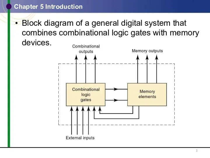
- 3. Chapter 5 Introduction Block diagram of a general digital system that combines combinational logic gates with
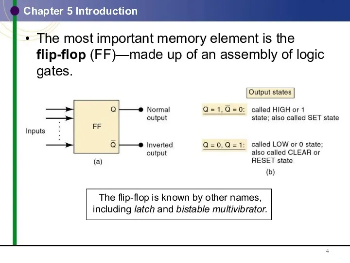
- 4. Chapter 5 Introduction The most important memory element is the flip-flop (FF)—made up of an assembly
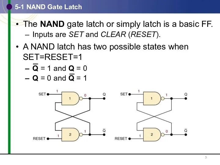
- 5. 5-1 NAND Gate Latch The NAND gate latch or simply latch is a basic FF. Inputs
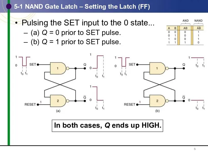
- 6. 5-1 NAND Gate Latch – Setting the Latch (FF) Pulsing the SET input to the 0
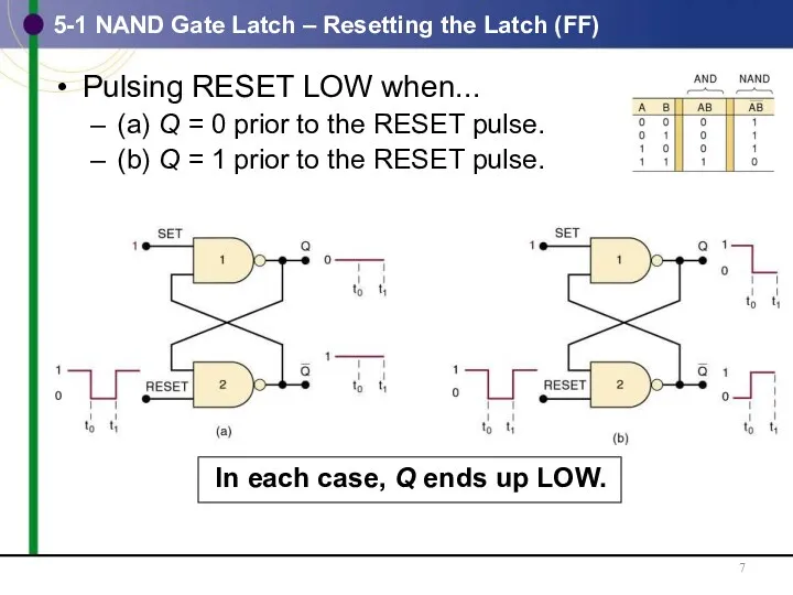
- 7. 5-1 NAND Gate Latch – Resetting the Latch (FF) Pulsing RESET LOW when... (a) Q =
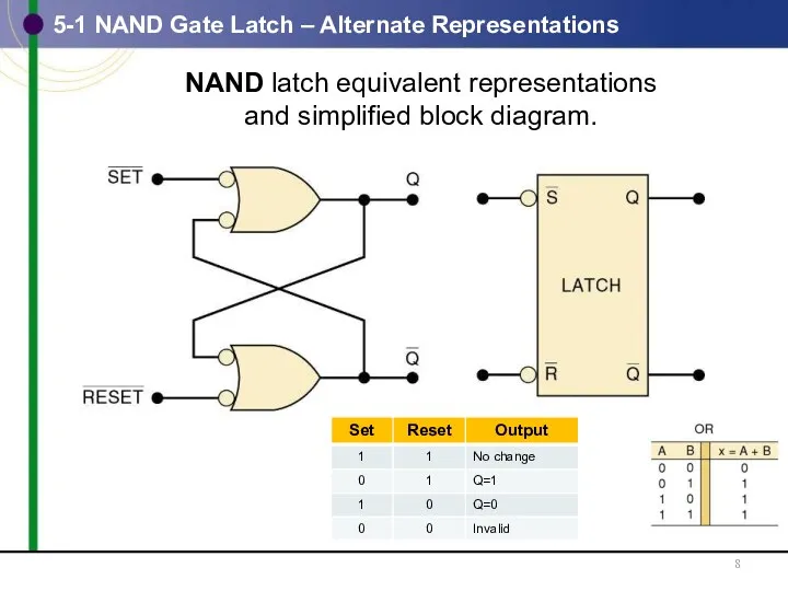
- 8. 5-1 NAND Gate Latch – Alternate Representations
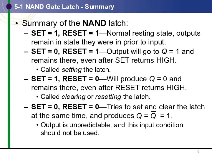
- 9. Summary of the NAND latch: SET = 1, RESET = 1—Normal resting state, outputs remain in
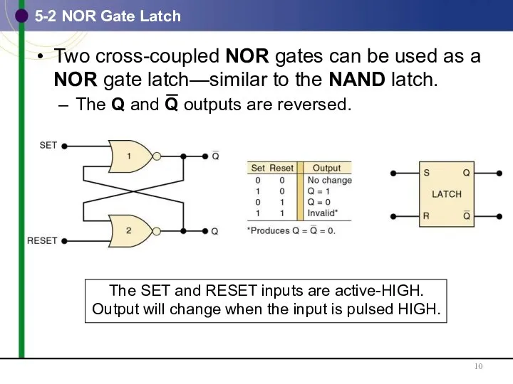
- 10. 5-2 NOR Gate Latch
- 11. 5-2 NOR Gate Latch - Summary Summary of the NOR latch: SET = 0, RESET =
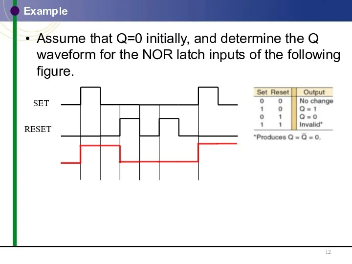
- 12. Example Assume that Q=0 initially, and determine the Q waveform for the NOR latch inputs of
- 13. 5-2 Power-Up When power is applied, it is not possible to predict the starting state of
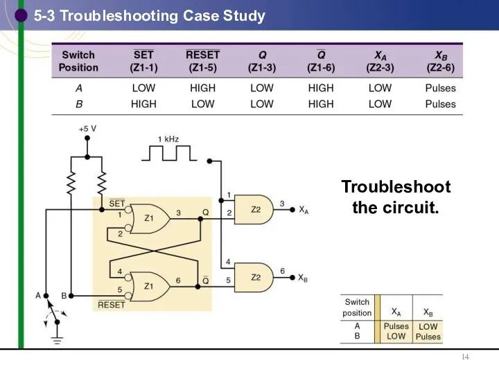
- 14. 5-3 Troubleshooting Case Study Troubleshoot the circuit.
- 15. 5-3 Troubleshooting Case Study There are several possibilities: An internal open connection at Z1-1, which would
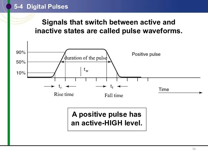
- 16. 5-4 Digital Pulses Signals that switch between active and inactive states are called pulse waveforms. Fall
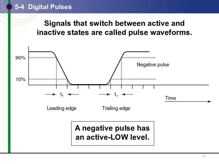
- 17. 5-4 Digital Pulses Signals that switch between active and inactive states are called pulse waveforms.
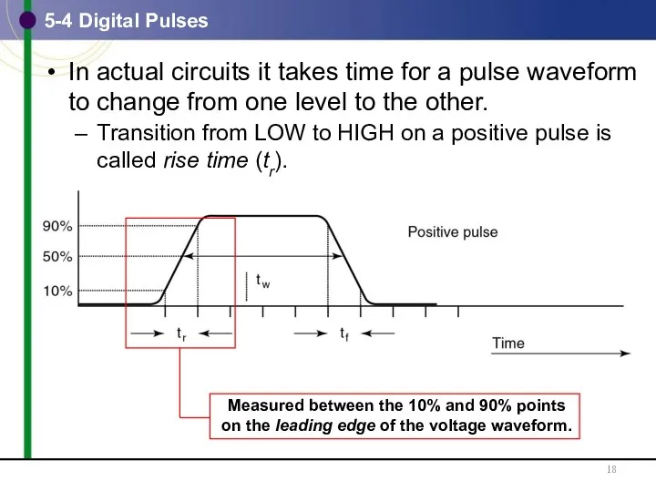
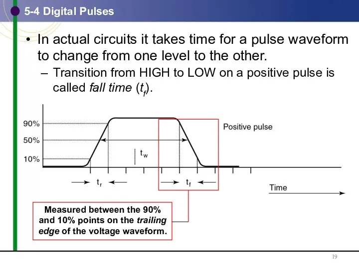
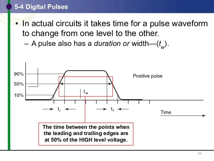
- 18. 5-4 Digital Pulses In actual circuits it takes time for a pulse waveform to change from
- 19. 5-4 Digital Pulses In actual circuits it takes time for a pulse waveform to change from
- 20. 5-4 Digital Pulses In actual circuits it takes time for a pulse waveform to change from
- 21. 5-5 Clock Signals and Clocked Flip-Flops Digital systems can operate either asynchronously or synchronously. Asynchronous system—outputs
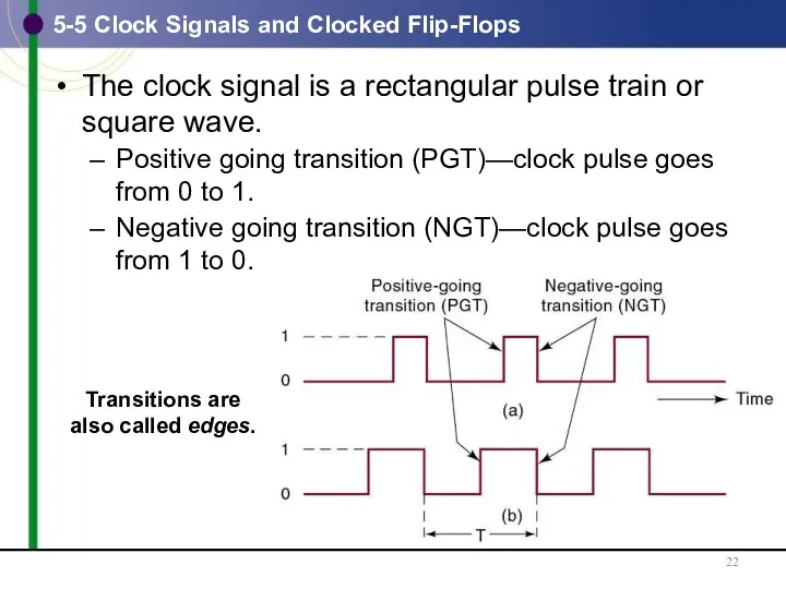
- 22. 5-5 Clock Signals and Clocked Flip-Flops The clock signal is a rectangular pulse train or square
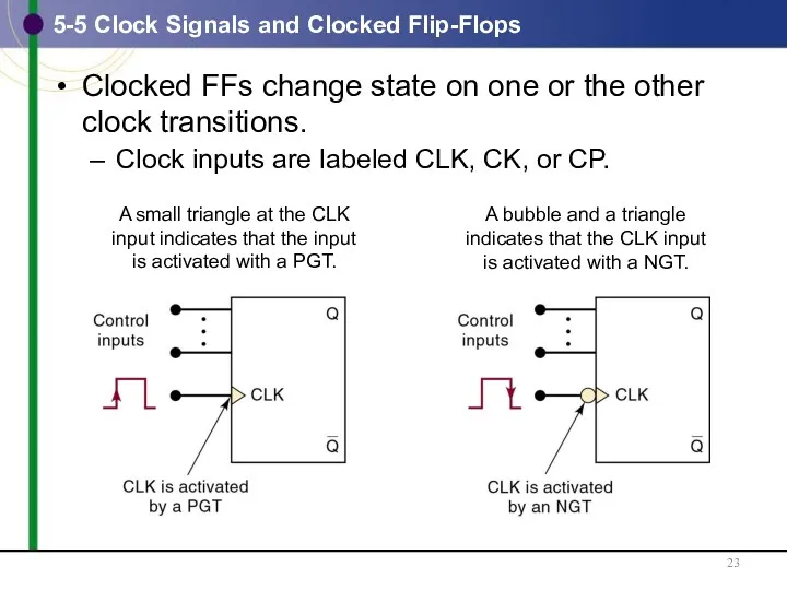
- 23. 5-5 Clock Signals and Clocked Flip-Flops Clocked FFs change state on one or the other clock
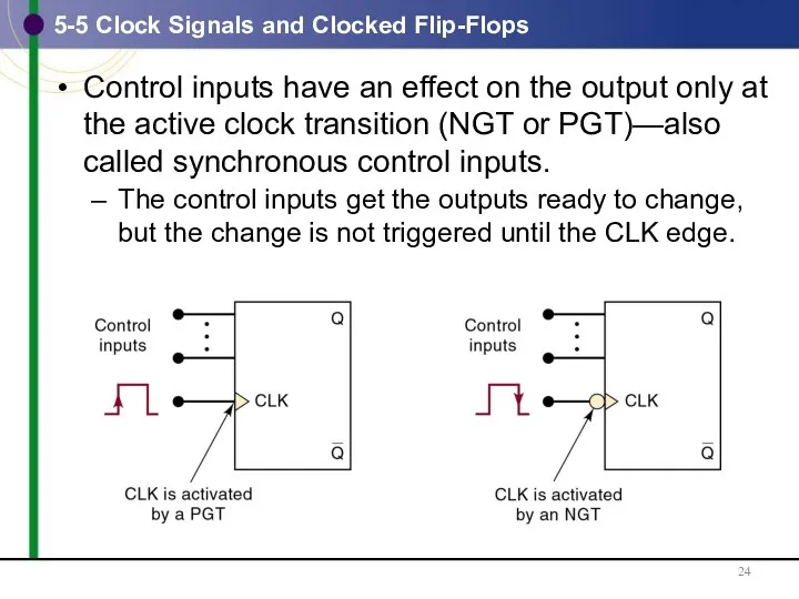
- 24. 5-5 Clock Signals and Clocked Flip-Flops Control inputs have an effect on the output only at
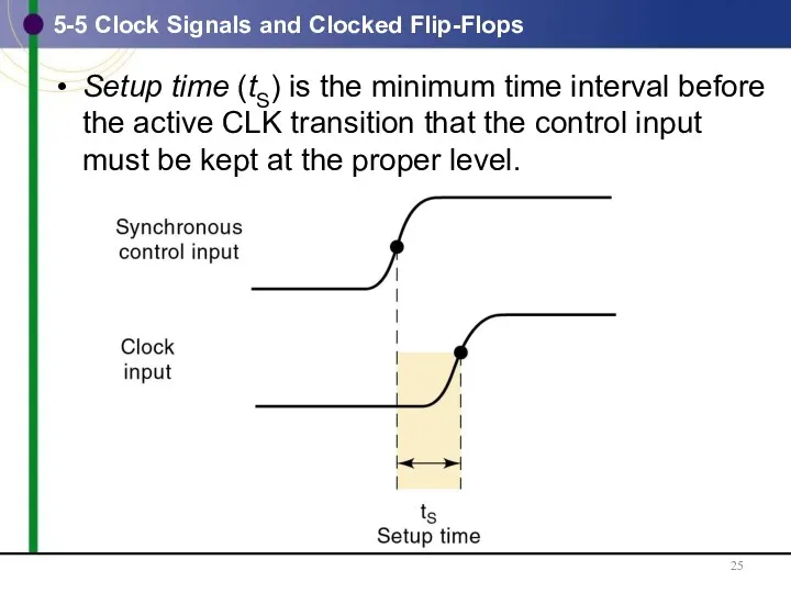
- 25. 5-5 Clock Signals and Clocked Flip-Flops Setup time (tS) is the minimum time interval before the
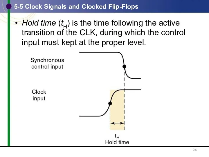
- 26. 5-5 Clock Signals and Clocked Flip-Flops Hold time (tH) is the time following the active transition
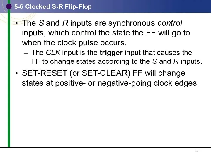
- 27. 5-6 Clocked S-R Flip-Flop The S and R inputs are synchronous control inputs, which control the
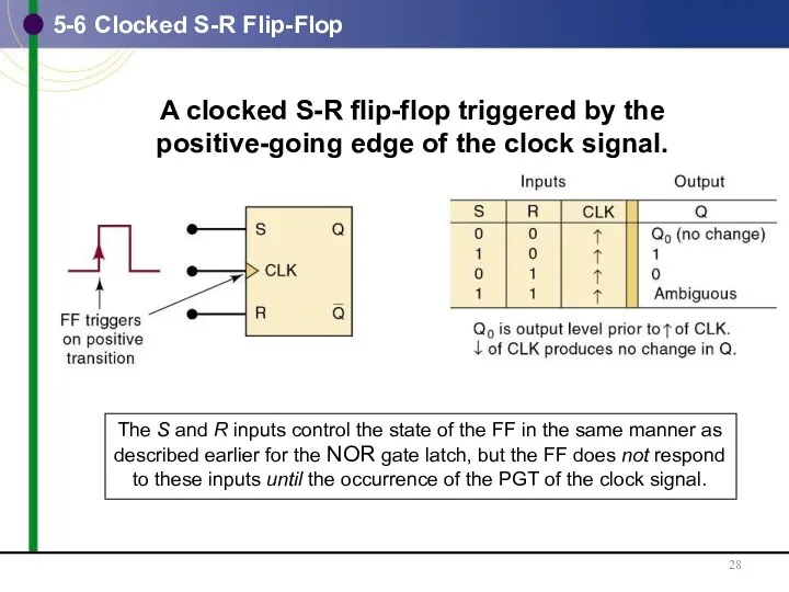
- 28. 5-6 Clocked S-R Flip-Flop A clocked S-R flip-flop triggered by the positive-going edge of the clock
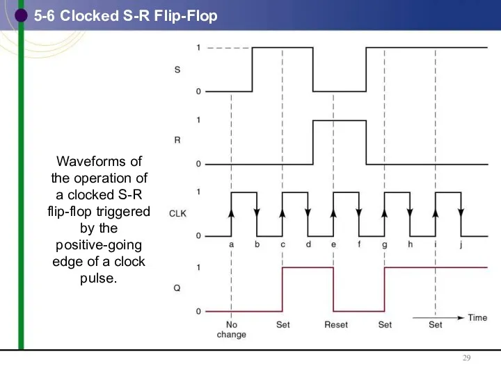
- 29. 5-6 Clocked S-R Flip-Flop Waveforms of the operation of a clocked S-R flip-flop triggered by the
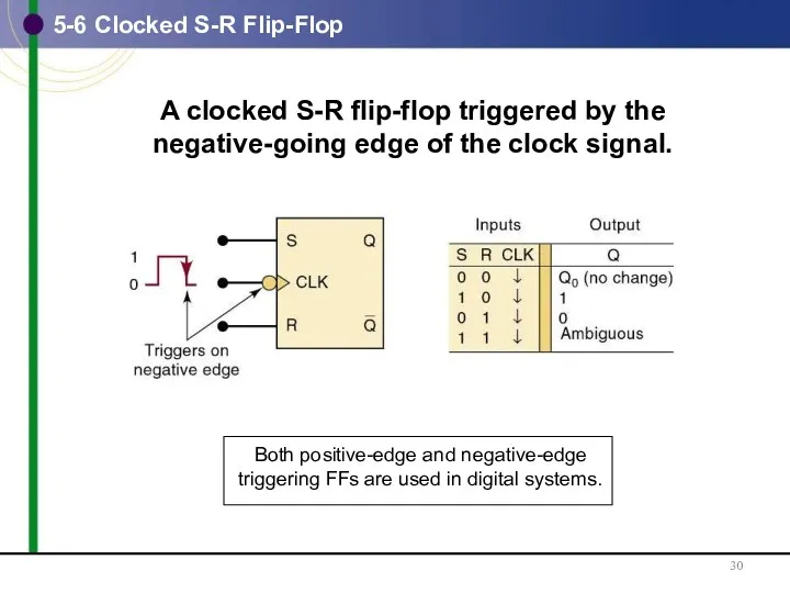
- 30. 5-6 Clocked S-R Flip-Flop A clocked S-R flip-flop triggered by the negative-going edge of the clock
- 31. 5-6 Clocked S-R Flip-Flop – Internal Circuitry An edge-triggered S-R flip-flop circuit features: A basic NAND
- 32. 5-6 Clocked S-R Flip-Flop – Internal Circuitry Implementation of edge-detector circuits used in edge-triggered flip-flops: (a)
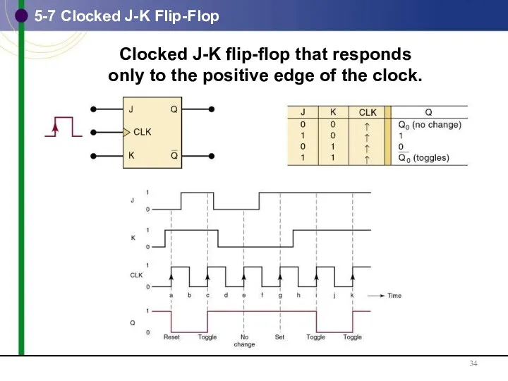
- 33. 5-7 Clocked J-K Flip-Flop Operates like the S-R FF. J is SET, K is CLEAR. When
- 34. 5-7 Clocked J-K Flip-Flop Clocked J-K flip-flop that responds only to the positive edge of the
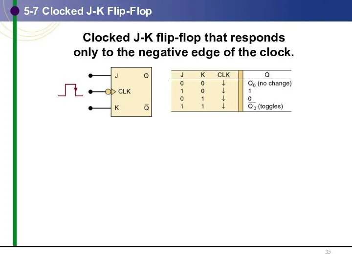
- 35. 5-7 Clocked J-K Flip-Flop Clocked J-K flip-flop that responds only to the negative edge of the
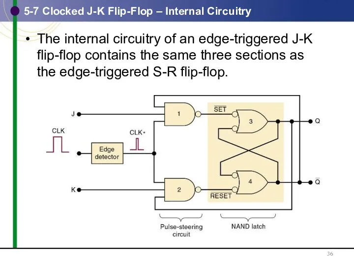
- 36. 5-7 Clocked J-K Flip-Flop – Internal Circuitry The internal circuitry of an edge-triggered J-K flip-flop contains
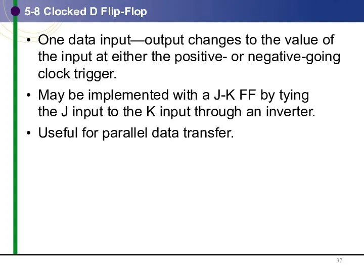
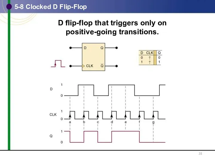
- 37. 5-8 Clocked D Flip-Flop One data input—output changes to the value of the input at either
- 38. 5-8 Clocked D Flip-Flop D flip-flop that triggers only on positive-going transitions.
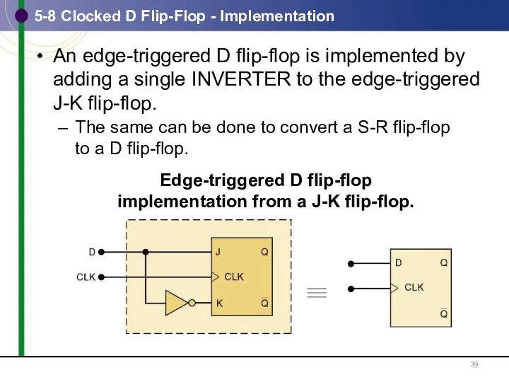
- 39. 5-8 Clocked D Flip-Flop - Implementation An edge-triggered D flip-flop is implemented by adding a single
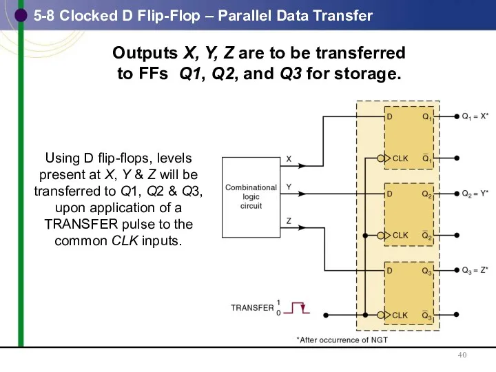
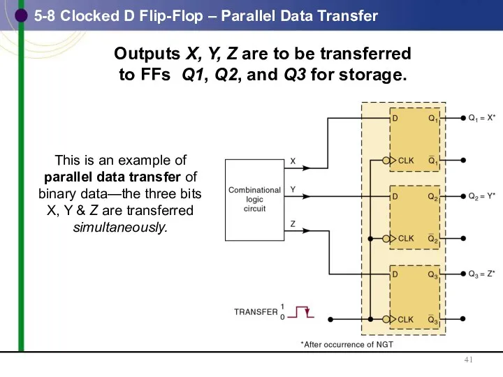
- 40. 5-8 Clocked D Flip-Flop – Parallel Data Transfer Outputs X, Y, Z are to be transferred
- 41. 5-8 Clocked D Flip-Flop – Parallel Data Transfer Outputs X, Y, Z are to be transferred
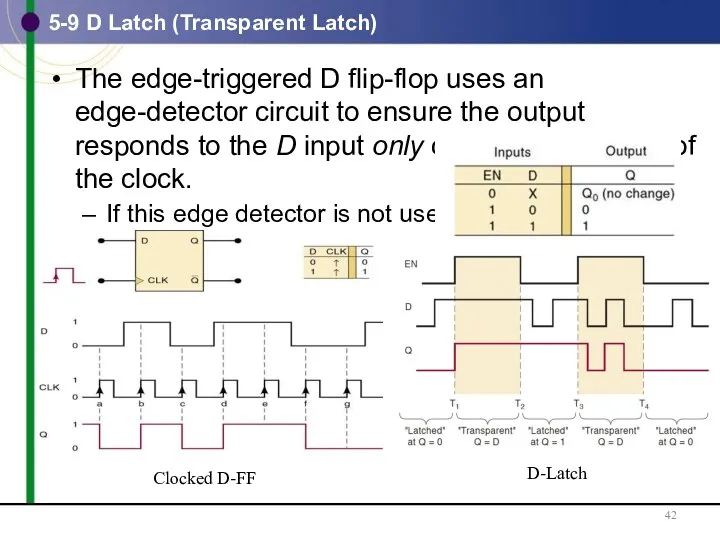
- 42. 5-9 D Latch (Transparent Latch) The edge-triggered D flip-flop uses an edge-detector circuit to ensure the
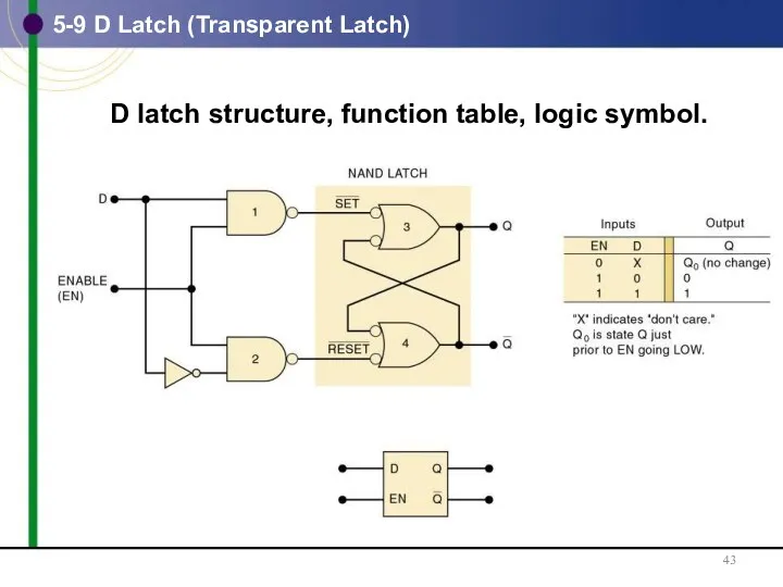
- 43. 5-9 D Latch (Transparent Latch) D latch structure, function table, logic symbol.
- 44. 5-9 D Latch (Transparent Latch) The circuit contains the NAND latch and the steering NAND gates
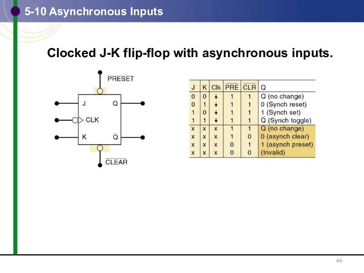
- 45. 5-10 Asynchronous Inputs Inputs that depend on the clock are synchronous. Most clocked FFs have asynchronous
- 46. 5-10 Asynchronous Inputs Clocked J-K flip-flop with asynchronous inputs.
- 47. 5-10 Asynchronous Inputs - Designations IC manufacturers do not agree on nomenclature for asynchronous inputs. The
- 48. 5-10 Asynchronous Inputs A J-K FF that responds to a NGT on its clock input and
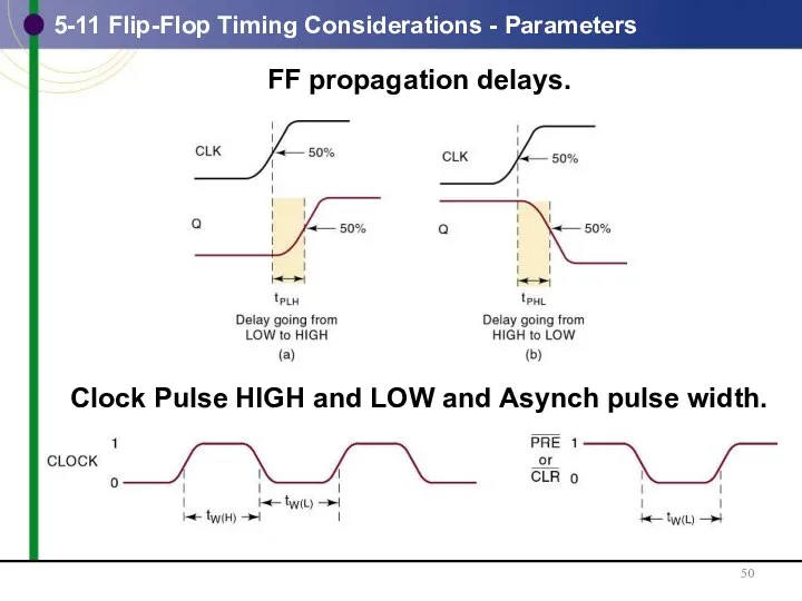
- 49. 5-11 Flip-Flop Timing Considerations - Parameters Important timing parameters: Setup and hold times Propagation delay—time for
- 50. 5-11 Flip-Flop Timing Considerations - Parameters FF propagation delays. Clock Pulse HIGH and LOW and Asynch
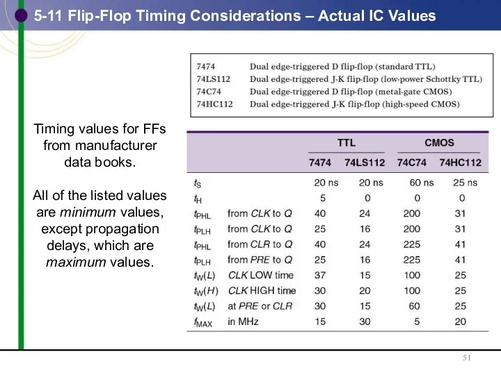
- 51. 5-11 Flip-Flop Timing Considerations – Actual IC Values
- 52. Example From the table in the previous page: Assume that Q=0. How long can it take
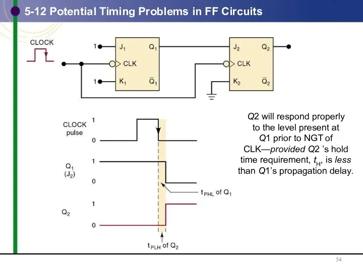
- 53. 5-12 Potential Timing Problems in FF Circuits When the output of one FF is connected to
- 54. 5-12 Potential Timing Problems in FF Circuits
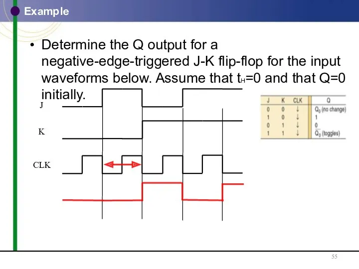
- 55. Example Determine the Q output for a negative-edge-triggered J-K flip-flop for the input waveforms below. Assume
- 56. 5-13 Flip-Flop Applications Examples of applications: Counting; Storing binary data Transferring binary data between locations Many
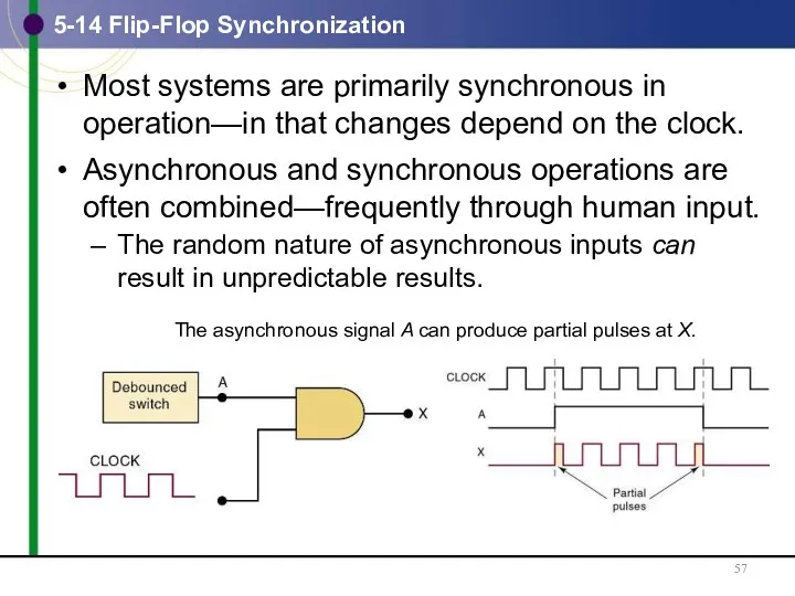
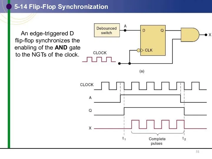
- 57. 5-14 Flip-Flop Synchronization Most systems are primarily synchronous in operation—in that changes depend on the clock.
- 58. 5-14 Flip-Flop Synchronization An edge-triggered D flip-flop synchronizes the enabling of the AND gate to the
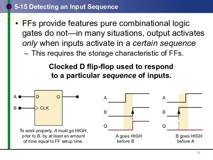
- 59. 5-15 Detecting an Input Sequence FFs provide features pure combinational logic gates do not—in many situations,
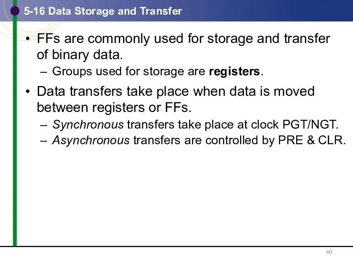
- 60. 5-16 Data Storage and Transfer FFs are commonly used for storage and transfer of binary data.
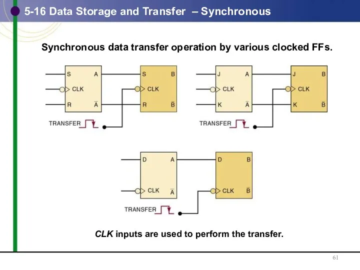
- 61. 5-16 Data Storage and Transfer – Synchronous
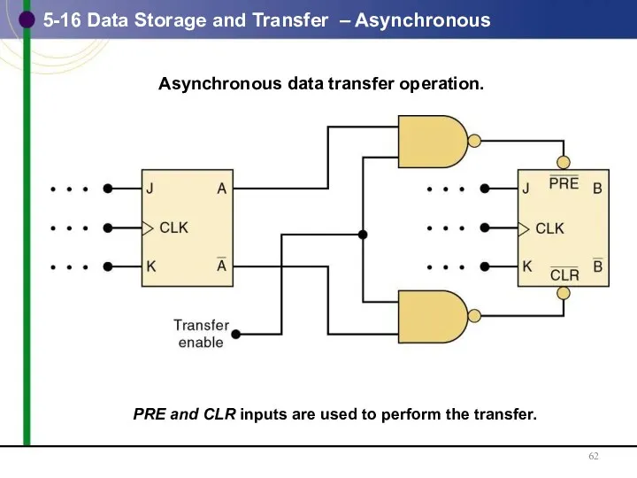
- 62. 5-16 Data Storage and Transfer – Asynchronous
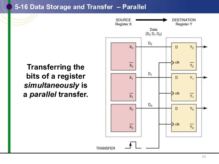
- 63. 5-16 Data Storage and Transfer – Parallel Transferring the bits of a register simultaneously is a
- 64. 5-17 Serial Data Transfer Transferring the bits of a register a bit at a time is
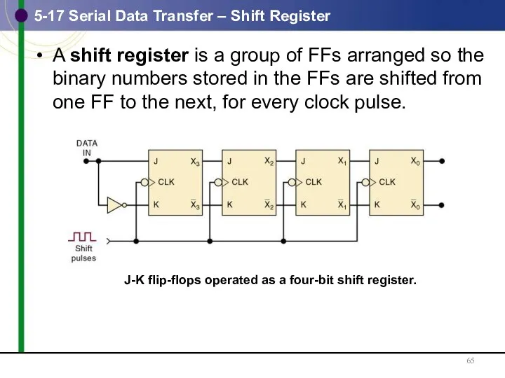
- 65. 5-17 Serial Data Transfer – Shift Register A shift register is a group of FFs arranged
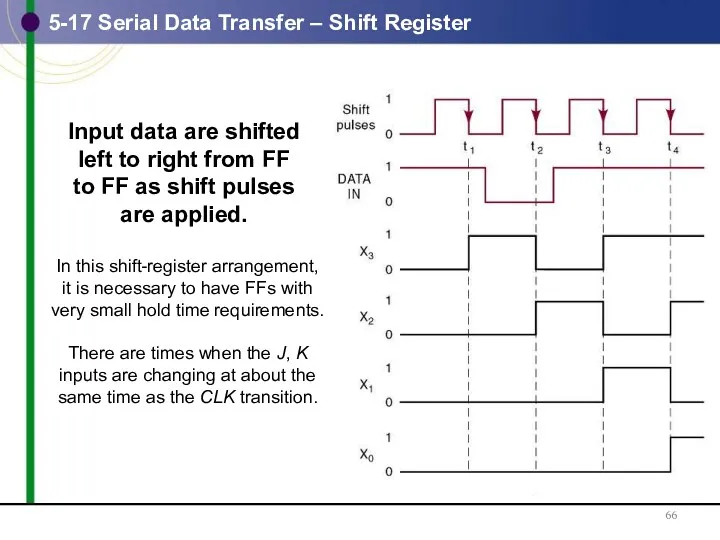
- 66. 5-17 Serial Data Transfer – Shift Register Input data are shifted left to right from FF
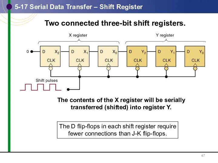
- 67. 5-17 Serial Data Transfer – Shift Register Two connected three-bit shift registers. The contents of the
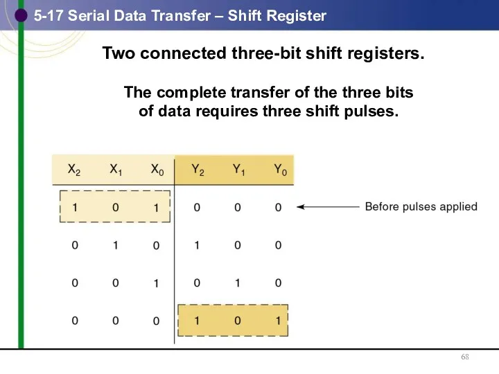
- 68. 5-17 Serial Data Transfer – Shift Register Two connected three-bit shift registers. The complete transfer of
- 69. 5-17 Serial Data Transfer – Shift Register Two connected three-bit shift registers. On each pulse NGT,
- 70. 5-17 Serial Data Transfer – Shift Register Two connected three-bit shift registers. On each pulse NGT,
- 71. 5-17 Serial Data Transfer – Shift Register Two connected three-bit shift registers. On each pulse NGT,
- 72. 5-17 Serial Data Transfer – Shift Register Two connected three-bit shift registers. The 101 stored in
- 73. 5-17 Serial Data Transfer vs. Parallel FFs can just as easily be connected so that information
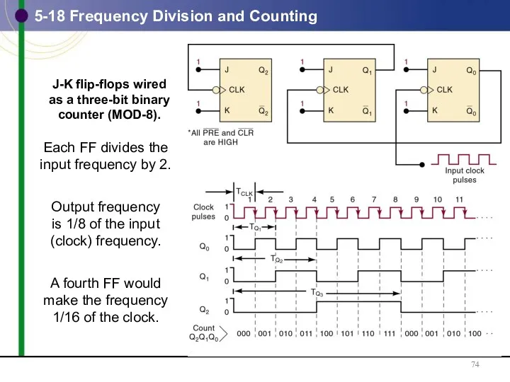
- 74. 5-18 Frequency Division and Counting J-K flip-flops wired as a three-bit binary counter (MOD-8). Each FF
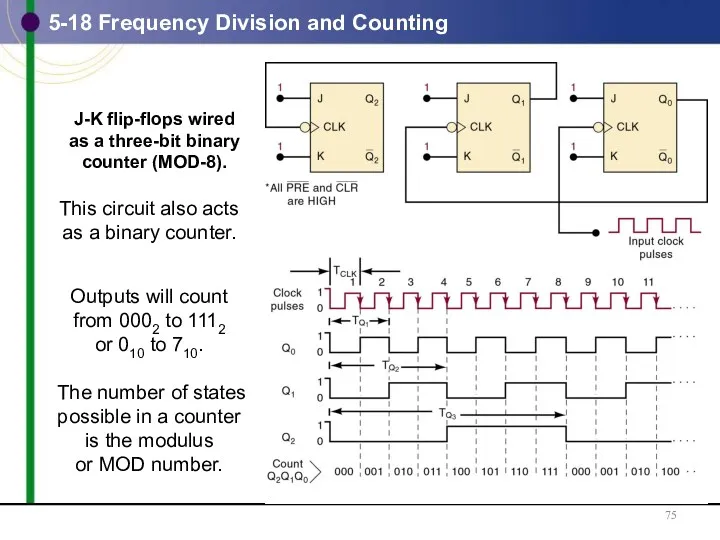
- 75. 5-18 Frequency Division and Counting J-K flip-flops wired as a three-bit binary counter (MOD-8). This circuit
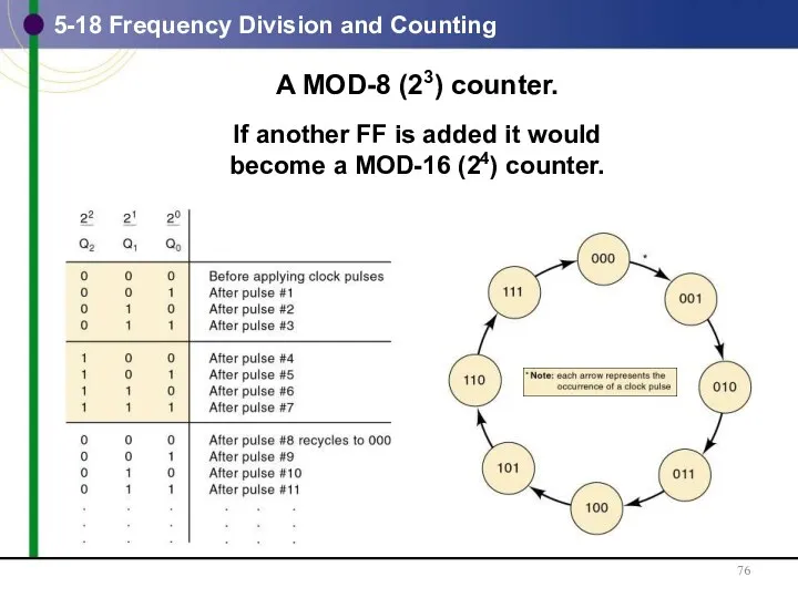
- 76. 5-18 Frequency Division and Counting A MOD-8 (23) counter. If another FF is added it would
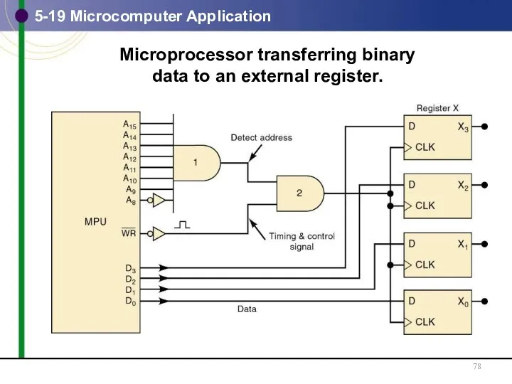
- 77. 5-19 Microcomputer Application Microprocessor units (MPUs) perform many functions involving use of registers for data transfer
- 78. 5-19 Microcomputer Application Microprocessor transferring binary data to an external register.
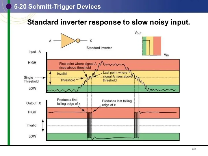
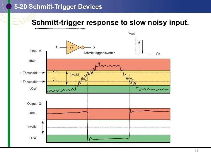
- 79. 5-20 Schmitt-Trigger Devices Not classified as a FF—but has a useful memory characteristic in certain situations.
- 80. 5-20 Schmitt-Trigger Devices Standard inverter response to slow noisy input.
- 81. 5-20 Schmitt-Trigger Devices Schmitt-trigger response to slow noisy input.
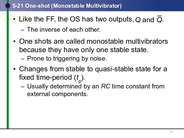
- 82. One shots are called monostable multivibrators because they have only one stable state. Prone to triggering
- 83. Nonretriggerable devices trigger & return to stable. Retriggerable devices can be triggered while in the quasi-stable
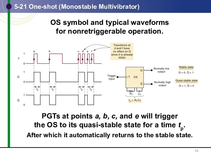
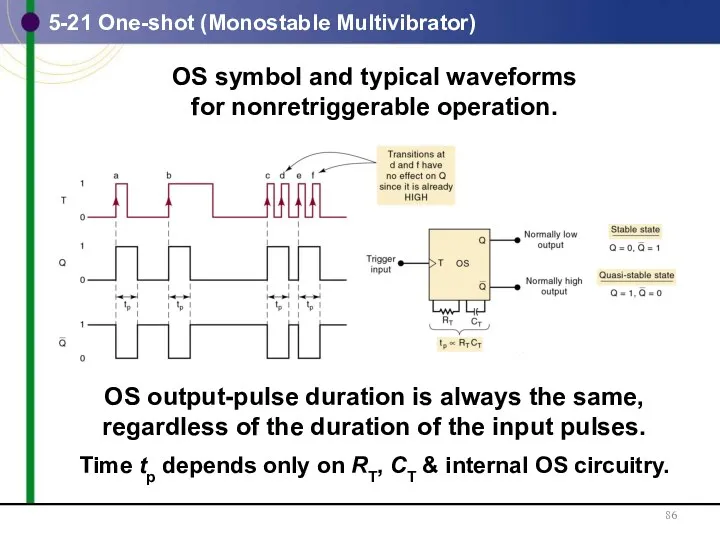
- 84. 5-21 One-shot (Monostable Multivibrator) OS symbol and typical waveforms for nonretriggerable operation. PGTs at points a,
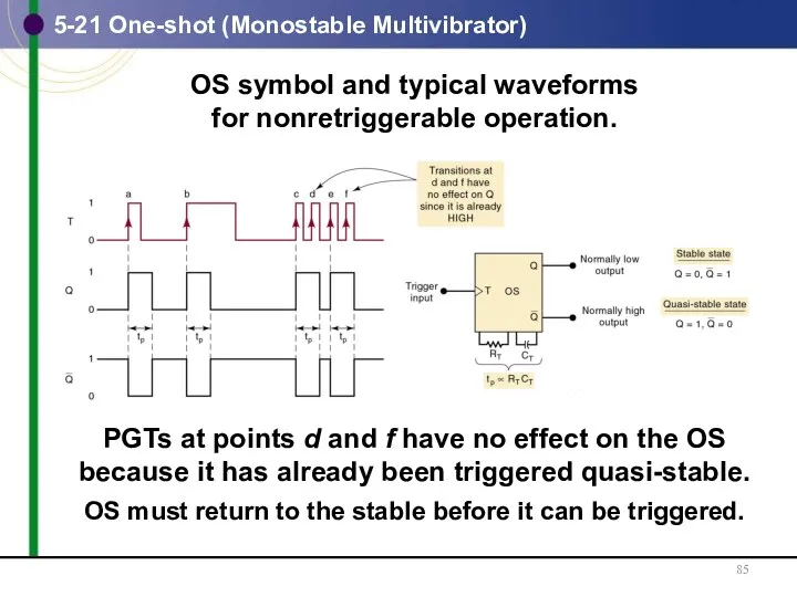
- 85. 5-21 One-shot (Monostable Multivibrator) OS symbol and typical waveforms for nonretriggerable operation. PGTs at points d
- 86. 5-21 One-shot (Monostable Multivibrator) OS symbol and typical waveforms for nonretriggerable operation. OS output-pulse duration is
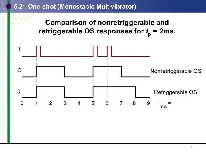
- 87. Comparison of nonretriggerable and retriggerable OS responses for tp = 2ms. 5-21 One-shot (Monostable Multivibrator)
- 88. Retriggerable OS begins a new tp interval each time it receives a trigger pulse. 5-21 One-shot
- 89. 74121 nonretriggerable one-shot IC. 5-21 One-shot (Monostable Multivibrator) Contains internal logic gates to allow inputs A1
- 90. 5-22 Clock Generator Circuits A third type multivibrator has no stable states—an astable or free-running multivibrator.
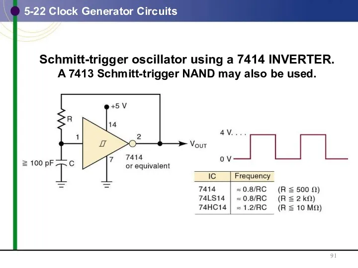
- 91. 5-22 Clock Generator Circuits Schmitt-trigger oscillator using a 7414 INVERTER. A 7413 Schmitt-trigger NAND may also
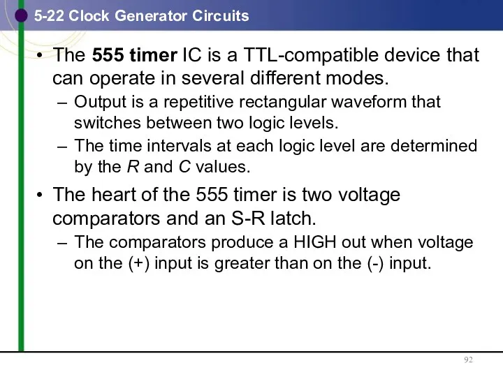
- 92. 5-22 Clock Generator Circuits The 555 timer IC is a TTL-compatible device that can operate in
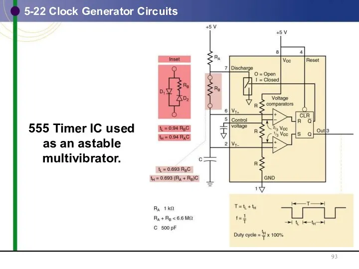
- 93. 5-22 Clock Generator Circuits 555 Timer IC used as an astable multivibrator.
- 94. 5-22 Clock Generator Circuits Crystal control may be used if a very stable clock is needed—used
- 95. 5-23 Troubleshooting Flip-Flop Circuits FFs are subject to the same faults that occur in combinational logic
- 96. 5-23 Troubleshooting Flip-Flop Circuits Clock skew occurs when CLK signals arrive at different FFs at different
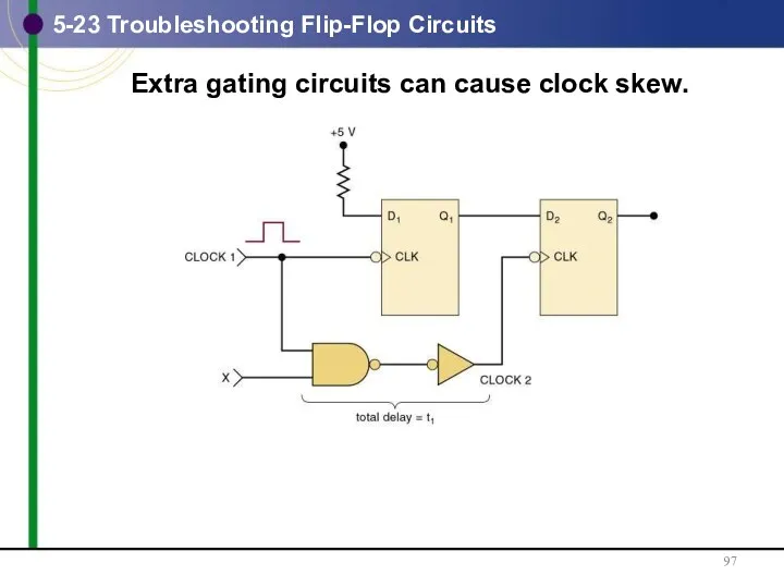
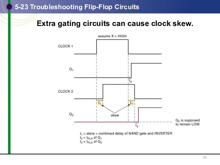
- 97. 5-23 Troubleshooting Flip-Flop Circuits Extra gating circuits can cause clock skew.
- 98. 5-23 Troubleshooting Flip-Flop Circuits Extra gating circuits can cause clock skew.
- 100. Скачать презентацию
Selected areas covered in this chapter:
Constructing/analyzing operation of latch flip-flops made from NAND
Selected areas covered in this chapter:
Constructing/analyzing operation of latch flip-flops made from NAND
Chapter 5 Introduction
Block diagram of a general digital system that combines combinational logic
Chapter 5 Introduction
Block diagram of a general digital system that combines combinational logic
Chapter 5 Introduction
The most important memory element is the flip-flop (FF)—made up of
Chapter 5 Introduction
The most important memory element is the flip-flop (FF)—made up of
5-1 NAND Gate Latch
The NAND gate latch or simply latch is a basic
5-1 NAND Gate Latch
The NAND gate latch or simply latch is a basic
5-1 NAND Gate Latch – Setting the Latch (FF)
Pulsing the SET input to
5-1 NAND Gate Latch – Setting the Latch (FF)
Pulsing the SET input to
5-1 NAND Gate Latch – Resetting the Latch (FF)
Pulsing RESET LOW when...
(a) Q
5-1 NAND Gate Latch – Resetting the Latch (FF)
Pulsing RESET LOW when...
(a) Q
5-1 NAND Gate Latch – Alternate Representations
5-1 NAND Gate Latch – Alternate Representations
Summary of the NAND latch:
SET = 1, RESET = 1—Normal resting state, outputs
Summary of the NAND latch:
SET = 1, RESET = 1—Normal resting state, outputs
5-2 NOR Gate Latch
5-2 NOR Gate Latch
5-2 NOR Gate Latch - Summary
Summary of the NOR latch:
SET = 0, RESET
5-2 NOR Gate Latch - Summary
Summary of the NOR latch:
SET = 0, RESET
Example
Assume that Q=0 initially, and determine the Q waveform for the NOR latch
Example
Assume that Q=0 initially, and determine the Q waveform for the NOR latch
5-2 Power-Up
When power is applied, it is not possible to predict the starting
5-2 Power-Up
When power is applied, it is not possible to predict the starting
5-3 Troubleshooting Case Study
Troubleshoot
the circuit.
5-3 Troubleshooting Case Study
Troubleshoot
the circuit.
5-3 Troubleshooting Case Study
There are several possibilities:
An internal open connection at Z1-1, which
5-3 Troubleshooting Case Study
There are several possibilities:
An internal open connection at Z1-1, which
5-4 Digital Pulses
Signals that switch between active and
inactive states are called pulse waveforms.
Fall
5-4 Digital Pulses
Signals that switch between active and
inactive states are called pulse waveforms.
Fall
5-4 Digital Pulses
Signals that switch between active and
inactive states are called pulse waveforms.
5-4 Digital Pulses
Signals that switch between active and
inactive states are called pulse waveforms.
5-4 Digital Pulses
In actual circuits it takes time for a pulse waveform to
5-4 Digital Pulses
In actual circuits it takes time for a pulse waveform to
5-4 Digital Pulses
In actual circuits it takes time for a pulse waveform to
5-4 Digital Pulses
In actual circuits it takes time for a pulse waveform to
5-4 Digital Pulses
In actual circuits it takes time for a pulse waveform to
5-4 Digital Pulses
In actual circuits it takes time for a pulse waveform to
5-5 Clock Signals and Clocked Flip-Flops
Digital systems can operate either asynchronously or synchronously.
Asynchronous
5-5 Clock Signals and Clocked Flip-Flops
Digital systems can operate either asynchronously or synchronously.
Asynchronous
5-5 Clock Signals and Clocked Flip-Flops
The clock signal is a rectangular pulse train
5-5 Clock Signals and Clocked Flip-Flops
The clock signal is a rectangular pulse train
5-5 Clock Signals and Clocked Flip-Flops
Clocked FFs change state on one or the
5-5 Clock Signals and Clocked Flip-Flops
Clocked FFs change state on one or the
5-5 Clock Signals and Clocked Flip-Flops
Control inputs have an effect on the output
5-5 Clock Signals and Clocked Flip-Flops
Control inputs have an effect on the output
5-5 Clock Signals and Clocked Flip-Flops
Setup time (tS) is the minimum time interval
5-5 Clock Signals and Clocked Flip-Flops
Setup time (tS) is the minimum time interval
5-5 Clock Signals and Clocked Flip-Flops
Hold time (tH) is the time following the
5-5 Clock Signals and Clocked Flip-Flops
Hold time (tH) is the time following the
5-6 Clocked S-R Flip-Flop
The S and R inputs are synchronous control inputs, which
5-6 Clocked S-R Flip-Flop
The S and R inputs are synchronous control inputs, which
5-6 Clocked S-R Flip-Flop
A clocked S-R flip-flop triggered by the
positive-going edge of the
5-6 Clocked S-R Flip-Flop
A clocked S-R flip-flop triggered by the positive-going edge of the
5-6 Clocked S-R Flip-Flop
Waveforms of
the operation of
a clocked S-R
flip-flop triggered by the positive-going
5-6 Clocked S-R Flip-Flop
Waveforms of the operation of a clocked S-R flip-flop triggered by the positive-going
5-6 Clocked S-R Flip-Flop
A clocked S-R flip-flop triggered by the
negative-going edge of the
5-6 Clocked S-R Flip-Flop
A clocked S-R flip-flop triggered by the negative-going edge of the
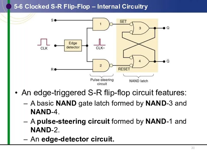
5-6 Clocked S-R Flip-Flop – Internal Circuitry
An edge-triggered S-R flip-flop circuit features:
A basic
5-6 Clocked S-R Flip-Flop – Internal Circuitry
An edge-triggered S-R flip-flop circuit features:
A basic
5-6 Clocked S-R Flip-Flop – Internal Circuitry
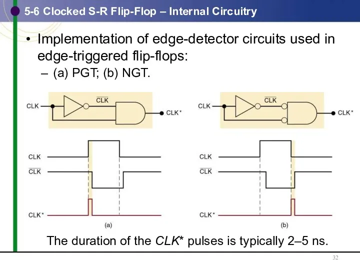
Implementation of edge-detector circuits used in edge-triggered
5-6 Clocked S-R Flip-Flop – Internal Circuitry
Implementation of edge-detector circuits used in edge-triggered
5-7 Clocked J-K Flip-Flop
Operates like the S-R FF.
J is SET, K is CLEAR.
When
5-7 Clocked J-K Flip-Flop
Operates like the S-R FF.
J is SET, K is CLEAR.
When
5-7 Clocked J-K Flip-Flop
Clocked J-K flip-flop that responds
only to the positive edge of
5-7 Clocked J-K Flip-Flop
Clocked J-K flip-flop that responds only to the positive edge of
5-7 Clocked J-K Flip-Flop
Clocked J-K flip-flop that responds
only to the negative edge of
5-7 Clocked J-K Flip-Flop
Clocked J-K flip-flop that responds only to the negative edge of
5-7 Clocked J-K Flip-Flop – Internal Circuitry
The internal circuitry of an edge-triggered J-K
flip-flop
5-7 Clocked J-K Flip-Flop – Internal Circuitry
The internal circuitry of an edge-triggered J-K flip-flop
5-8 Clocked D Flip-Flop
One data input—output changes to the value of the input
5-8 Clocked D Flip-Flop
One data input—output changes to the value of the input
5-8 Clocked D Flip-Flop
D flip-flop that triggers only on
positive-going transitions.
5-8 Clocked D Flip-Flop
D flip-flop that triggers only on
positive-going transitions.
5-8 Clocked D Flip-Flop - Implementation
An edge-triggered D flip-flop is implemented by adding
5-8 Clocked D Flip-Flop - Implementation
An edge-triggered D flip-flop is implemented by adding
5-8 Clocked D Flip-Flop – Parallel Data Transfer
Outputs X, Y, Z are to
5-8 Clocked D Flip-Flop – Parallel Data Transfer
Outputs X, Y, Z are to
5-8 Clocked D Flip-Flop – Parallel Data Transfer
Outputs X, Y, Z are to
5-8 Clocked D Flip-Flop – Parallel Data Transfer
Outputs X, Y, Z are to
5-9 D Latch (Transparent Latch)
The edge-triggered D flip-flop uses an edge-detector circuit to
5-9 D Latch (Transparent Latch)
The edge-triggered D flip-flop uses an edge-detector circuit to
5-9 D Latch (Transparent Latch)
D latch structure, function table, logic symbol.
5-9 D Latch (Transparent Latch)
D latch structure, function table, logic symbol.
5-9 D Latch (Transparent Latch)
The circuit contains the NAND latch and the steering
5-9 D Latch (Transparent Latch)
The circuit contains the NAND latch and the steering
5-10 Asynchronous Inputs
Inputs that depend on the clock are synchronous.
Most clocked FFs have
5-10 Asynchronous Inputs
Inputs that depend on the clock are synchronous.
Most clocked FFs have
5-10 Asynchronous Inputs
Clocked J-K flip-flop with asynchronous inputs.
5-10 Asynchronous Inputs
Clocked J-K flip-flop with asynchronous inputs.
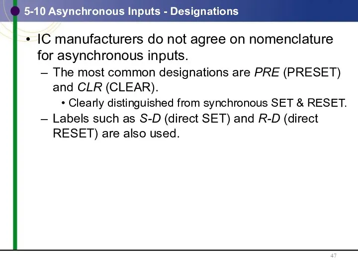
5-10 Asynchronous Inputs - Designations
IC manufacturers do not agree on nomenclature for asynchronous
5-10 Asynchronous Inputs - Designations
IC manufacturers do not agree on nomenclature for asynchronous
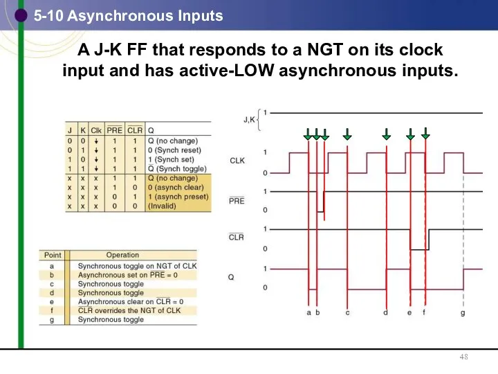
5-10 Asynchronous Inputs
A J-K FF that responds to a NGT on its clock
input
5-10 Asynchronous Inputs
A J-K FF that responds to a NGT on its clock input
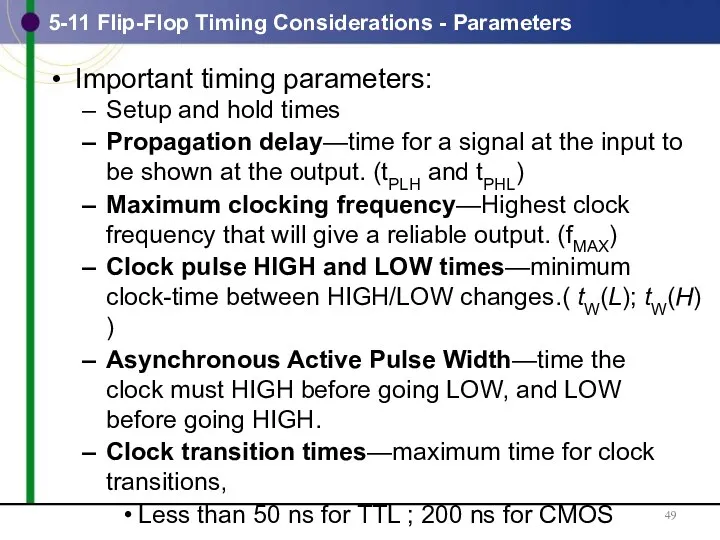
5-11 Flip-Flop Timing Considerations - Parameters
Important timing parameters:
Setup and hold times
Propagation delay—time for
5-11 Flip-Flop Timing Considerations - Parameters
Important timing parameters:
Setup and hold times
Propagation delay—time for
5-11 Flip-Flop Timing Considerations - Parameters
FF propagation delays.
Clock Pulse HIGH and LOW and
5-11 Flip-Flop Timing Considerations - Parameters
FF propagation delays.
Clock Pulse HIGH and LOW and
5-11 Flip-Flop Timing Considerations – Actual IC Values
5-11 Flip-Flop Timing Considerations – Actual IC Values
Example
From the table in the previous page:
Assume that Q=0. How long can it
Example
From the table in the previous page:
Assume that Q=0. How long can it
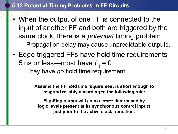
5-12 Potential Timing Problems in FF Circuits
When the output of one FF is
5-12 Potential Timing Problems in FF Circuits
When the output of one FF is
5-12 Potential Timing Problems in FF Circuits
5-12 Potential Timing Problems in FF Circuits
Example
Determine the Q output for a negative-edge-triggered J-K flip-flop for the input waveforms
Example
Determine the Q output for a negative-edge-triggered J-K flip-flop for the input waveforms
5-13 Flip-Flop Applications
Examples of applications:
Counting; Storing binary data
Transferring binary data between locations
Many FF
5-13 Flip-Flop Applications
Examples of applications:
Counting; Storing binary data
Transferring binary data between locations
Many FF
5-14 Flip-Flop Synchronization
Most systems are primarily synchronous in operation—in that changes depend on
5-14 Flip-Flop Synchronization
Most systems are primarily synchronous in operation—in that changes depend on
5-14 Flip-Flop Synchronization
An edge-triggered D flip-flop synchronizes the enabling of the AND gate
5-14 Flip-Flop Synchronization
An edge-triggered D flip-flop synchronizes the enabling of the AND gate
5-15 Detecting an Input Sequence
FFs provide features pure combinational logic gates do not—in
5-15 Detecting an Input Sequence
FFs provide features pure combinational logic gates do not—in
5-16 Data Storage and Transfer
FFs are commonly used for storage and transfer
of binary
5-16 Data Storage and Transfer
FFs are commonly used for storage and transfer of binary
5-16 Data Storage and Transfer – Synchronous
5-16 Data Storage and Transfer – Synchronous
5-16 Data Storage and Transfer – Asynchronous
5-16 Data Storage and Transfer – Asynchronous
5-16 Data Storage and Transfer – Parallel
Transferring the bits of a register simultaneously
5-16 Data Storage and Transfer – Parallel
Transferring the bits of a register simultaneously
5-17 Serial Data Transfer
Transferring the bits of a register a bit at a
5-17 Serial Data Transfer
Transferring the bits of a register a bit at a
5-17 Serial Data Transfer – Shift Register
A shift register is a group of
5-17 Serial Data Transfer – Shift Register
A shift register is a group of
5-17 Serial Data Transfer – Shift Register
Input data are shifted
left to right from
5-17 Serial Data Transfer – Shift Register
Input data are shifted left to right from
5-17 Serial Data Transfer – Shift Register
Two connected three-bit shift registers.
The contents of
5-17 Serial Data Transfer – Shift Register
Two connected three-bit shift registers.
The contents of
5-17 Serial Data Transfer – Shift Register
Two connected three-bit shift registers.
The complete transfer
5-17 Serial Data Transfer – Shift Register
Two connected three-bit shift registers.
The complete transfer
5-17 Serial Data Transfer – Shift Register
Two connected three-bit shift registers.
On each pulse
5-17 Serial Data Transfer – Shift Register
Two connected three-bit shift registers.
On each pulse
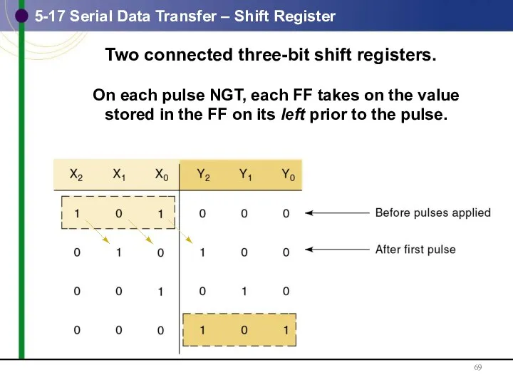
5-17 Serial Data Transfer – Shift Register
Two connected three-bit shift registers.
On each pulse
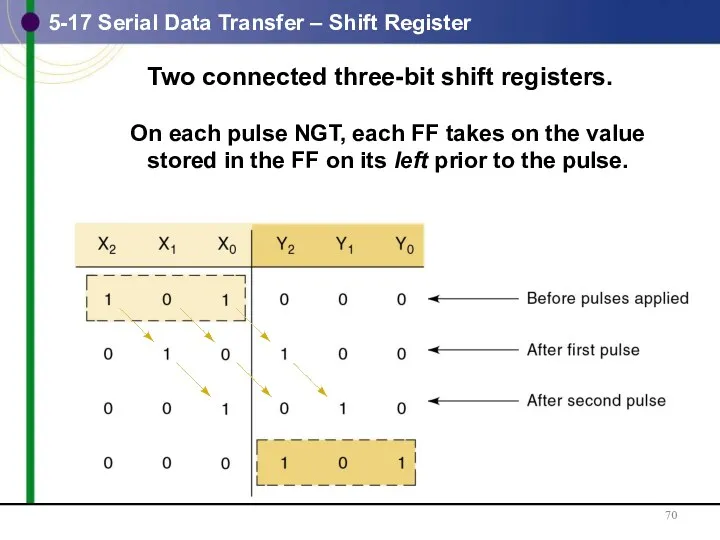
5-17 Serial Data Transfer – Shift Register
Two connected three-bit shift registers.
On each pulse
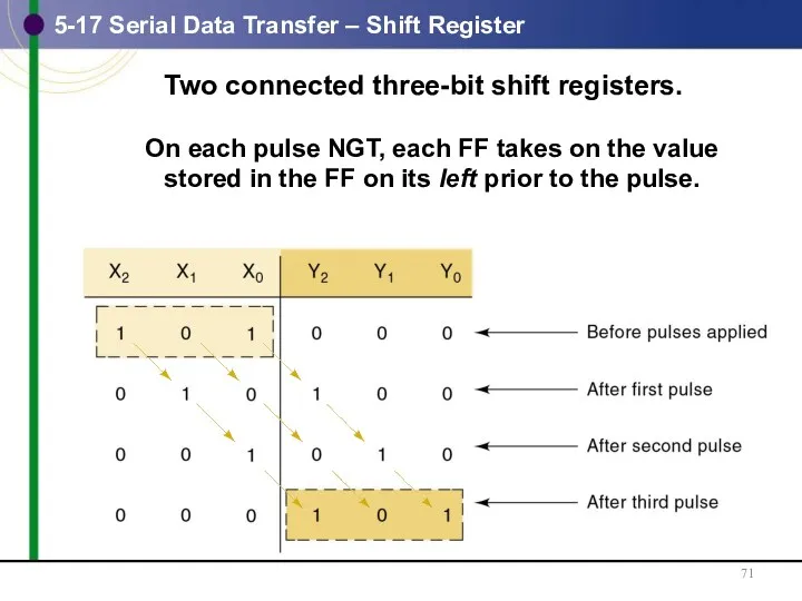
5-17 Serial Data Transfer – Shift Register
Two connected three-bit shift registers.
On each pulse
5-17 Serial Data Transfer – Shift Register
Two connected three-bit shift registers.
On each pulse
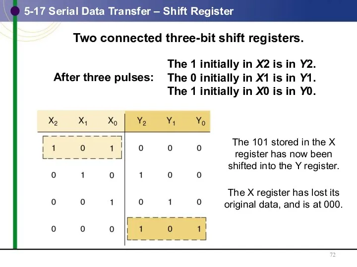
5-17 Serial Data Transfer – Shift Register
Two connected three-bit shift registers.
The 101 stored
5-17 Serial Data Transfer – Shift Register
Two connected three-bit shift registers.
The 101 stored
5-17 Serial Data Transfer vs. Parallel
FFs can just as easily be connected so
5-17 Serial Data Transfer vs. Parallel
FFs can just as easily be connected so
5-18 Frequency Division and Counting
J-K flip-flops wired
as a three-bit binary
counter (MOD-8).
Each FF divides
5-18 Frequency Division and Counting
J-K flip-flops wired
as a three-bit binary
counter (MOD-8).
Each FF divides
5-18 Frequency Division and Counting
J-K flip-flops wired
as a three-bit binary
counter (MOD-8).
This circuit also
5-18 Frequency Division and Counting
J-K flip-flops wired
as a three-bit binary
counter (MOD-8).
This circuit also
5-18 Frequency Division and Counting
A MOD-8 (23) counter.
If another FF is added
5-18 Frequency Division and Counting
A MOD-8 (23) counter.
If another FF is added
5-19 Microcomputer Application
Microprocessor units (MPUs) perform many functions involving use of registers for
5-19 Microcomputer Application
Microprocessor units (MPUs) perform many functions involving use of registers for
5-19 Microcomputer Application
Microprocessor transferring binary
data to an external register.
5-19 Microcomputer Application
Microprocessor transferring binary
data to an external register.
5-20 Schmitt-Trigger Devices
Not classified as a FF—but has a useful memory characteristic in
5-20 Schmitt-Trigger Devices
Not classified as a FF—but has a useful memory characteristic in
5-20 Schmitt-Trigger Devices
Standard inverter response to slow noisy input.
5-20 Schmitt-Trigger Devices
Standard inverter response to slow noisy input.
5-20 Schmitt-Trigger Devices
Schmitt-trigger response to slow noisy input.
5-20 Schmitt-Trigger Devices
Schmitt-trigger response to slow noisy input.
One shots are called monostable multivibrators because they have only one stable state.
Prone
One shots are called monostable multivibrators because they have only one stable state.
Prone
Nonretriggerable devices trigger & return to stable.
Retriggerable devices can be triggered while in
Nonretriggerable devices trigger & return to stable.
Retriggerable devices can be triggered while in
5-21 One-shot (Monostable Multivibrator)
OS symbol and typical waveforms
for nonretriggerable operation.
PGTs at points a,
5-21 One-shot (Monostable Multivibrator)
OS symbol and typical waveforms
for nonretriggerable operation.
PGTs at points a,
5-21 One-shot (Monostable Multivibrator)
OS symbol and typical waveforms
for nonretriggerable operation.
PGTs at points d
5-21 One-shot (Monostable Multivibrator)
OS symbol and typical waveforms
for nonretriggerable operation.
PGTs at points d
5-21 One-shot (Monostable Multivibrator)
OS symbol and typical waveforms
for nonretriggerable operation.
OS output-pulse duration is
5-21 One-shot (Monostable Multivibrator)
OS symbol and typical waveforms
for nonretriggerable operation.
OS output-pulse duration is
Comparison of nonretriggerable and
retriggerable OS responses for tp = 2ms.
5-21 One-shot (Monostable
Comparison of nonretriggerable and
retriggerable OS responses for tp = 2ms.
5-21 One-shot (Monostable
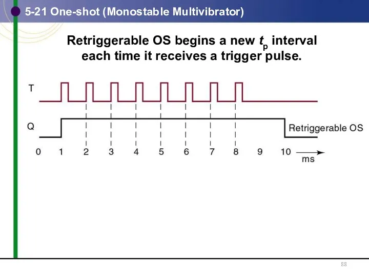
Retriggerable OS begins a new tp interval
each time it receives a trigger pulse.
Retriggerable OS begins a new tp interval each time it receives a trigger pulse.
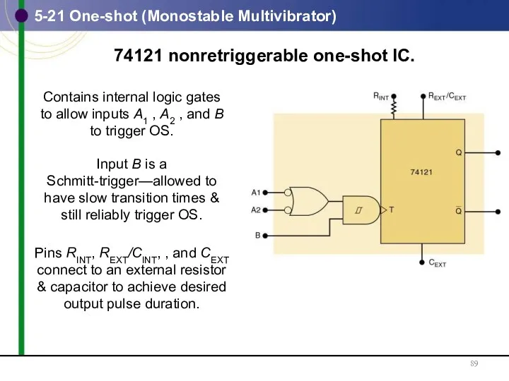
74121 nonretriggerable one-shot IC.
5-21 One-shot (Monostable Multivibrator)
Contains internal logic gates
to allow inputs
74121 nonretriggerable one-shot IC.
5-21 One-shot (Monostable Multivibrator)
Contains internal logic gates to allow inputs
5-22 Clock Generator Circuits
A third type multivibrator has no stable states—an astable or
5-22 Clock Generator Circuits
A third type multivibrator has no stable states—an astable or
5-22 Clock Generator Circuits
Schmitt-trigger oscillator using a 7414 INVERTER.
A 7413 Schmitt-trigger NAND may
5-22 Clock Generator Circuits
Schmitt-trigger oscillator using a 7414 INVERTER. A 7413 Schmitt-trigger NAND may
5-22 Clock Generator Circuits
The 555 timer IC is a TTL-compatible device that can
5-22 Clock Generator Circuits
The 555 timer IC is a TTL-compatible device that can
5-22 Clock Generator Circuits
555 Timer IC used as an astable multivibrator.
5-22 Clock Generator Circuits
555 Timer IC used as an astable multivibrator.
5-22 Clock Generator Circuits
Crystal control may be used if a very stable clock
5-22 Clock Generator Circuits
Crystal control may be used if a very stable clock
5-23 Troubleshooting Flip-Flop Circuits
FFs are subject to the same faults that occur in
5-23 Troubleshooting Flip-Flop Circuits
FFs are subject to the same faults that occur in
5-23 Troubleshooting Flip-Flop Circuits
Clock skew occurs when CLK signals arrive
at different FFs at
5-23 Troubleshooting Flip-Flop Circuits
Clock skew occurs when CLK signals arrive at different FFs at
5-23 Troubleshooting Flip-Flop Circuits
Extra gating circuits can cause clock skew.
5-23 Troubleshooting Flip-Flop Circuits
Extra gating circuits can cause clock skew.
5-23 Troubleshooting Flip-Flop Circuits
Extra gating circuits can cause clock skew.
5-23 Troubleshooting Flip-Flop Circuits
Extra gating circuits can cause clock skew.
 Государство Грузия
 Кинезиологические упражнения как средство активизации межполушарного взаимодействия и стимулирования познавательной деятельности.
 Методы анализа генома. Секвенирование
 Graphic Аrts
 Пожарная безопасность зданий. СНиП 21-01-97 Пожарная безопасность зданий и сооружений
 Дети с нарушениями психического развития (трудностями в обучении)
 Кристаллизация металла шва и образование трещин
 Консультация для педагогов Взаимодействие учителя-логопеда и специалистов по сопровождению детей с речевыми нарушениями в условиях ДОУ общеразвивающего вида (Форма организации: деловая игра Кто хочет стать профессионалом?).
 Инновационные приемы работы в рамках научно-исследовательской деятельности
 Презентация кабинета
 Презентации - МАФ 2022 Пивень А.В. (Вер 7)
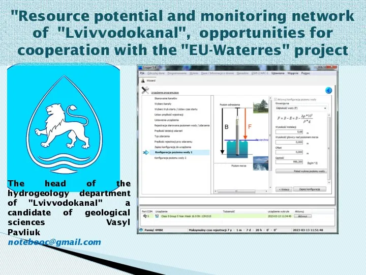 Resource potential and monitoring network of Lvivvodokanal, opportunities for cooperation with the EU-waterres project
 Основной государственный экзамен по русскому языку в 9 классе. Подготовка к написанию сочинения-рассуждения (15.2)
 Презентация проекта Золотая осень для воспитателей Доу
 Категория блага в истории этики и культуры
 Части речи
 Лексикалық қосымшалар тәсілі. Екінші тілдің тепе-тең бірліктерін іріктеп алу дағдысы
 В мире цирка
 Предложение ( 8 класс)
 Презентация Детские музыкальные инструменты своими руками
 Опыт работы по теме Деятельность классного руководителя по формированию нравственного поведения младших школьников
 Русские музыкальные инструменты
 Создание изделий из текстильных материалов. Конструирование юбок
 Автоматизация звука Р
 Теоретические основы производства азотной кислоты
 тыва дылга кичээл Темачангыс аймак кежигуннерлиг состер 7класс презентация
 Грыжи межпозвонковых дисков
 Лекция_4_Моделирование_соединений