- Digital systems. Flip - flops and related devices (chapter 5)

Содержание
- 2. Selected areas covered in this chapter: Constructing/analyzing operation of latch flip-flops made from NAND or NOR
- 3. Chapter 5 Introduction Block diagram of a general digital system that combines combinational logic gates with
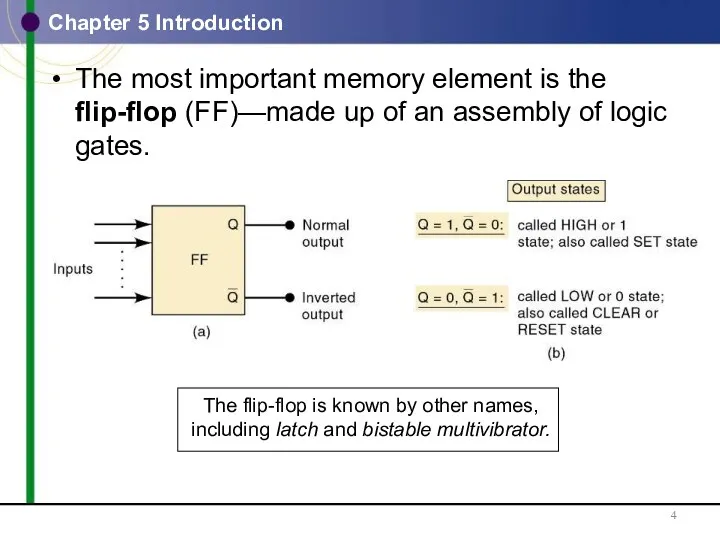
- 4. Chapter 5 Introduction The most important memory element is the flip-flop (FF)—made up of an assembly
- 5. 5-1 NAND Gate Latch The NAND gate latch or simply latch is a basic FF. Inputs
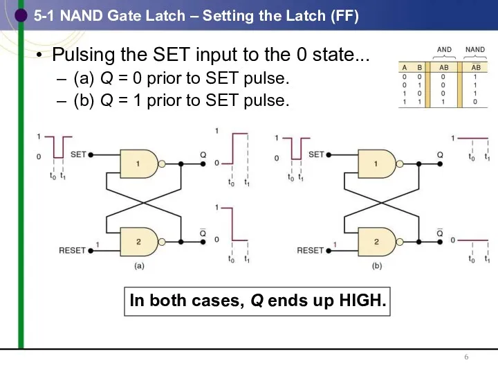
- 6. 5-1 NAND Gate Latch – Setting the Latch (FF) Pulsing the SET input to the 0
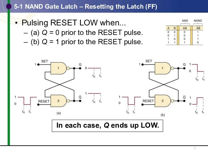
- 7. 5-1 NAND Gate Latch – Resetting the Latch (FF) Pulsing RESET LOW when... (a) Q =
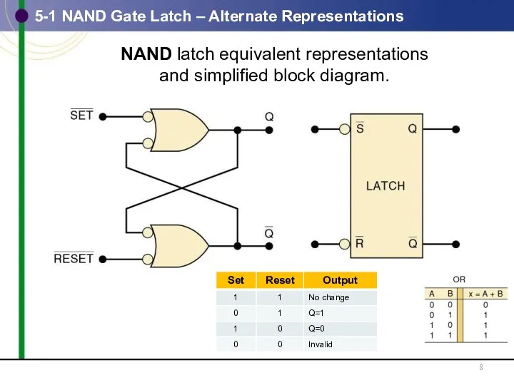
- 8. 5-1 NAND Gate Latch – Alternate Representations
- 9. Summary of the NAND latch: SET = 1, RESET = 1—Normal resting state, outputs remain in
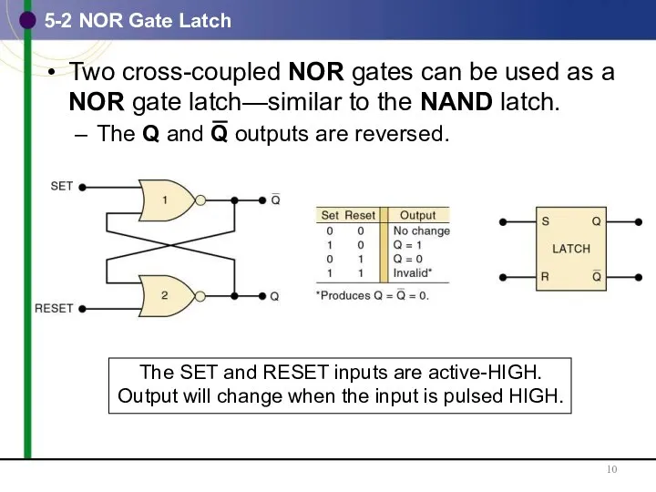
- 10. 5-2 NOR Gate Latch
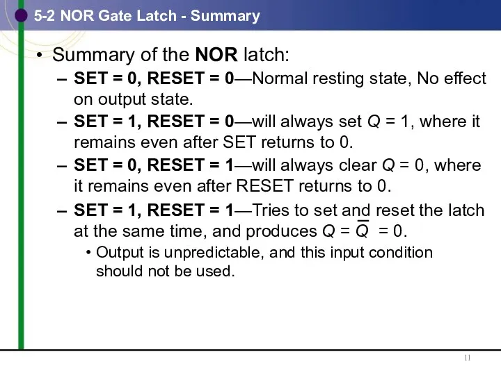
- 11. 5-2 NOR Gate Latch - Summary Summary of the NOR latch: SET = 0, RESET =
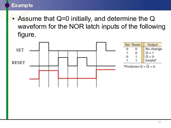
- 12. Example Assume that Q=0 initially, and determine the Q waveform for the NOR latch inputs of
- 13. 5-2 Power-Up When power is applied, it is not possible to predict the starting state of
- 14. 5-3 Troubleshooting Case Study Troubleshoot the circuit.
- 15. 5-3 Troubleshooting Case Study There are several possibilities: An internal open connection at Z1-1, which would
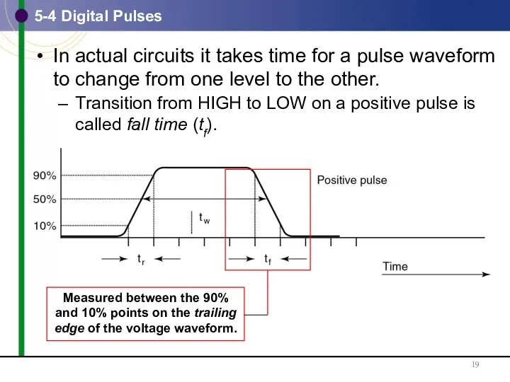
- 16. 5-4 Digital Pulses Signals that switch between active and inactive states are called pulse waveforms. Fall
- 17. 5-4 Digital Pulses Signals that switch between active and inactive states are called pulse waveforms.
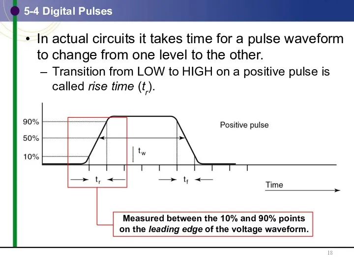
- 18. 5-4 Digital Pulses In actual circuits it takes time for a pulse waveform to change from
- 19. 5-4 Digital Pulses In actual circuits it takes time for a pulse waveform to change from
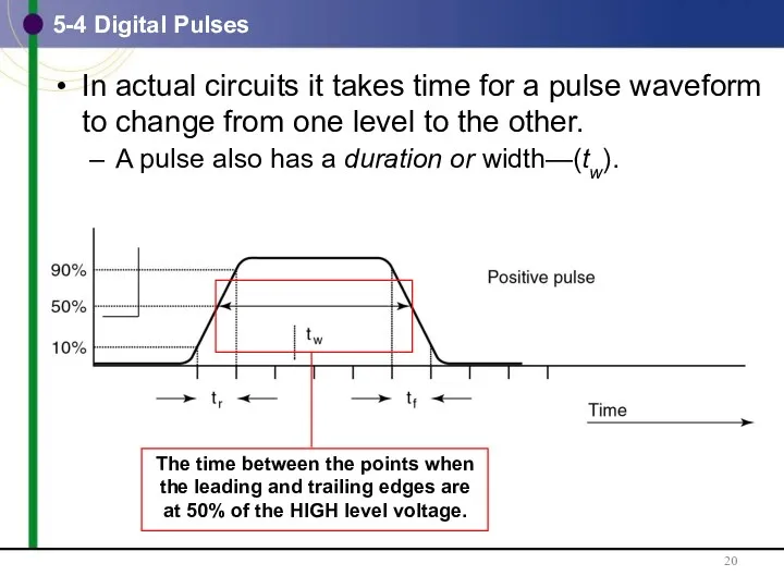
- 20. 5-4 Digital Pulses In actual circuits it takes time for a pulse waveform to change from
- 21. 5-5 Clock Signals and Clocked Flip-Flops Digital systems can operate either asynchronously or synchronously. Asynchronous system—outputs
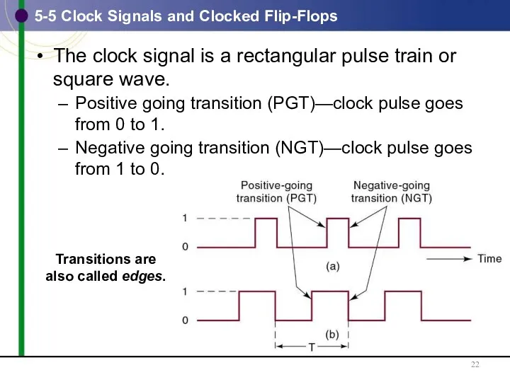
- 22. 5-5 Clock Signals and Clocked Flip-Flops The clock signal is a rectangular pulse train or square
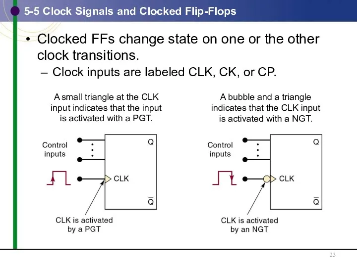
- 23. 5-5 Clock Signals and Clocked Flip-Flops Clocked FFs change state on one or the other clock
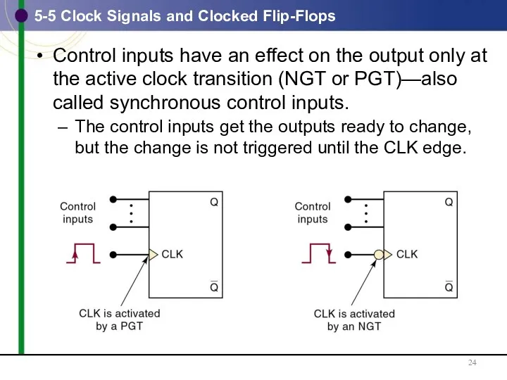
- 24. 5-5 Clock Signals and Clocked Flip-Flops Control inputs have an effect on the output only at
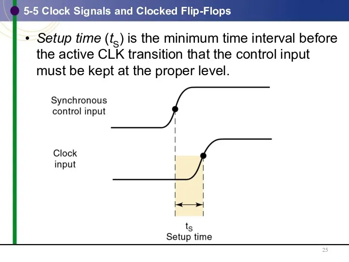
- 25. 5-5 Clock Signals and Clocked Flip-Flops Setup time (tS) is the minimum time interval before the
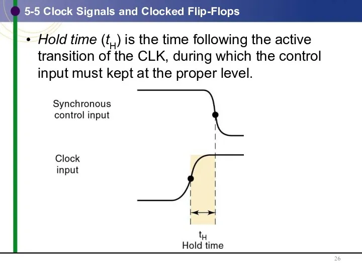
- 26. 5-5 Clock Signals and Clocked Flip-Flops Hold time (tH) is the time following the active transition
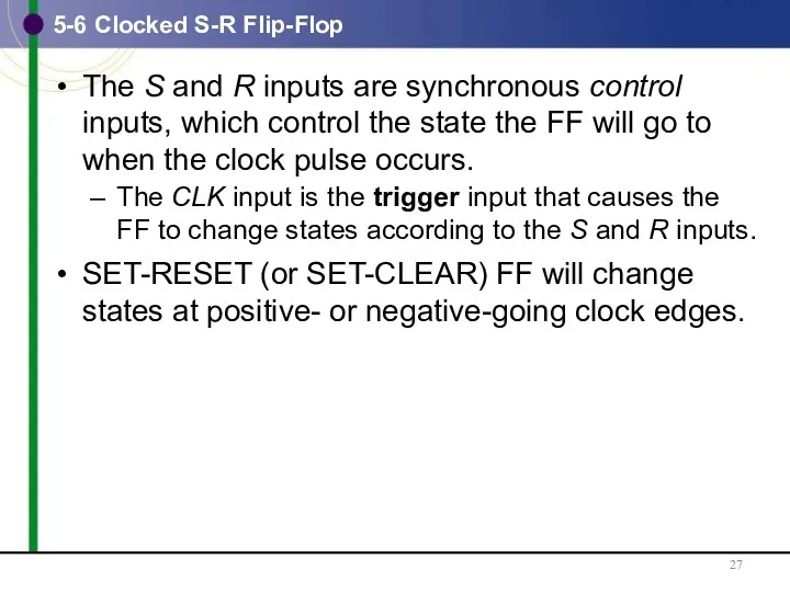
- 27. 5-6 Clocked S-R Flip-Flop The S and R inputs are synchronous control inputs, which control the
- 28. 5-6 Clocked S-R Flip-Flop A clocked S-R flip-flop triggered by the positive-going edge of the clock
- 29. 5-6 Clocked S-R Flip-Flop Waveforms of the operation of a clocked S-R flip-flop triggered by the
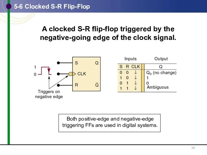
- 30. 5-6 Clocked S-R Flip-Flop A clocked S-R flip-flop triggered by the negative-going edge of the clock
- 31. 5-6 Clocked S-R Flip-Flop – Internal Circuitry An edge-triggered S-R flip-flop circuit features: A basic NAND
- 32. 5-6 Clocked S-R Flip-Flop – Internal Circuitry Implementation of edge-detector circuits used in edge-triggered flip-flops: (a)
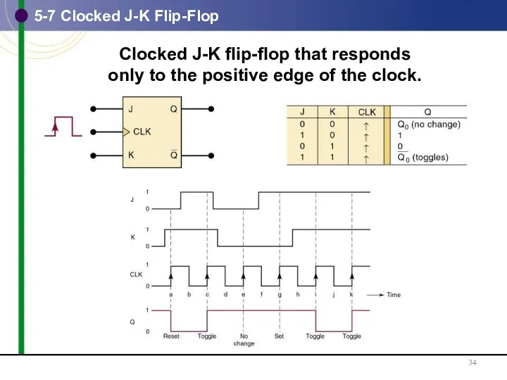
- 33. 5-7 Clocked J-K Flip-Flop Operates like the S-R FF. J is SET, K is CLEAR. When
- 34. 5-7 Clocked J-K Flip-Flop Clocked J-K flip-flop that responds only to the positive edge of the
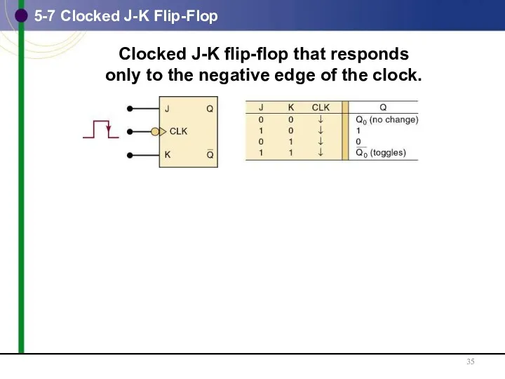
- 35. 5-7 Clocked J-K Flip-Flop Clocked J-K flip-flop that responds only to the negative edge of the
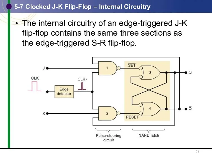
- 36. 5-7 Clocked J-K Flip-Flop – Internal Circuitry The internal circuitry of an edge-triggered J-K flip-flop contains
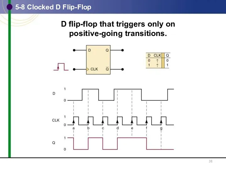
- 37. 5-8 Clocked D Flip-Flop One data input—output changes to the value of the input at either
- 38. 5-8 Clocked D Flip-Flop D flip-flop that triggers only on positive-going transitions.
- 39. 5-8 Clocked D Flip-Flop - Implementation An edge-triggered D flip-flop is implemented by adding a single
- 40. 5-8 Clocked D Flip-Flop – Parallel Data Transfer Outputs X, Y, Z are to be transferred
- 41. 5-8 Clocked D Flip-Flop – Parallel Data Transfer Outputs X, Y, Z are to be transferred
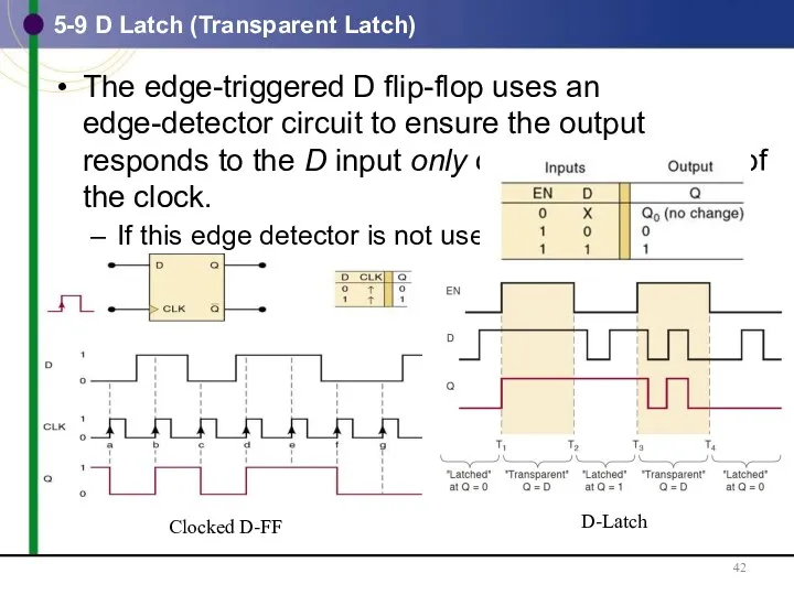
- 42. 5-9 D Latch (Transparent Latch) The edge-triggered D flip-flop uses an edge-detector circuit to ensure the
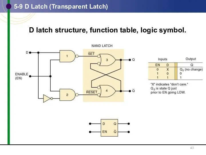
- 43. 5-9 D Latch (Transparent Latch) D latch structure, function table, logic symbol.
- 44. 5-9 D Latch (Transparent Latch) The circuit contains the NAND latch and the steering NAND gates
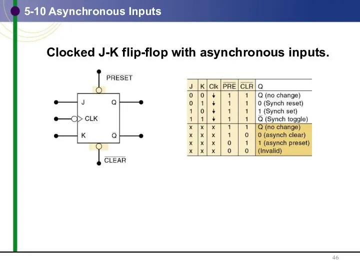
- 45. 5-10 Asynchronous Inputs Inputs that depend on the clock are synchronous. Most clocked FFs have asynchronous
- 46. 5-10 Asynchronous Inputs Clocked J-K flip-flop with asynchronous inputs.
- 47. 5-10 Asynchronous Inputs - Designations IC manufacturers do not agree on nomenclature for asynchronous inputs. The
- 48. 5-10 Asynchronous Inputs A J-K FF that responds to a NGT on its clock input and
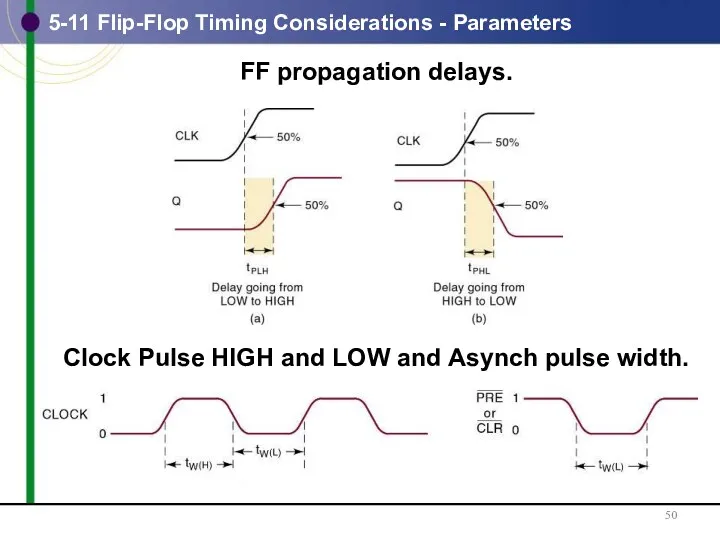
- 49. 5-11 Flip-Flop Timing Considerations - Parameters Important timing parameters: Setup and hold times Propagation delay—time for
- 50. 5-11 Flip-Flop Timing Considerations - Parameters FF propagation delays. Clock Pulse HIGH and LOW and Asynch
- 51. 5-11 Flip-Flop Timing Considerations – Actual IC Values
- 52. Example From the table in the previous page: Assume that Q=0. How long can it take
- 53. 5-12 Potential Timing Problems in FF Circuits When the output of one FF is connected to
- 54. 5-12 Potential Timing Problems in FF Circuits
- 55. Example Determine the Q output for a negative-edge-triggered J-K flip-flop for the input waveforms below. Assume
- 56. 5-13 Flip-Flop Applications Examples of applications: Counting; Storing binary data Transferring binary data between locations Many
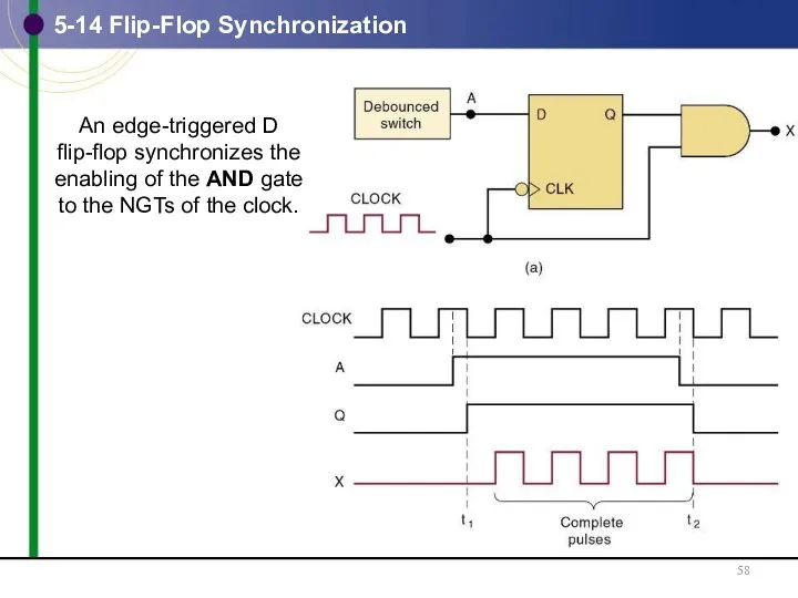
- 57. 5-14 Flip-Flop Synchronization Most systems are primarily synchronous in operation—in that changes depend on the clock.
- 58. 5-14 Flip-Flop Synchronization An edge-triggered D flip-flop synchronizes the enabling of the AND gate to the
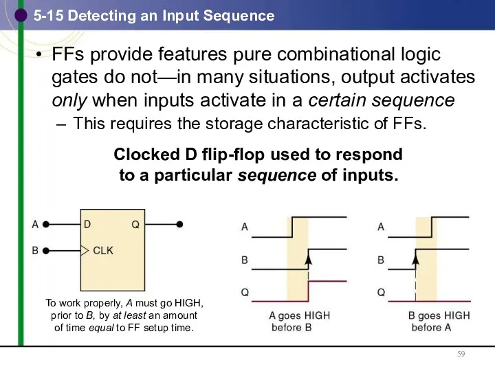
- 59. 5-15 Detecting an Input Sequence FFs provide features pure combinational logic gates do not—in many situations,
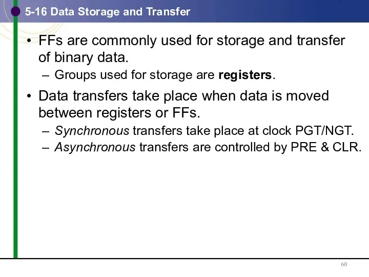
- 60. 5-16 Data Storage and Transfer FFs are commonly used for storage and transfer of binary data.
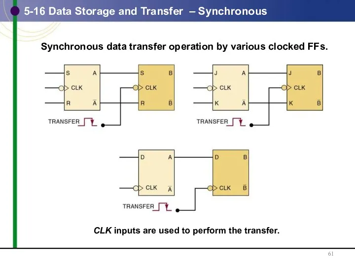
- 61. 5-16 Data Storage and Transfer – Synchronous
- 62. 5-16 Data Storage and Transfer – Asynchronous
- 63. 5-16 Data Storage and Transfer – Parallel Transferring the bits of a register simultaneously is a
- 64. 5-17 Serial Data Transfer Transferring the bits of a register a bit at a time is
- 65. 5-17 Serial Data Transfer – Shift Register A shift register is a group of FFs arranged
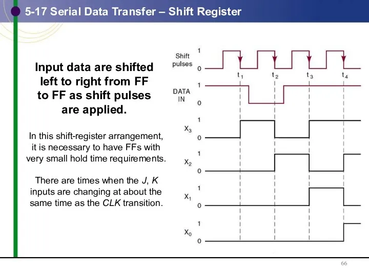
- 66. 5-17 Serial Data Transfer – Shift Register Input data are shifted left to right from FF
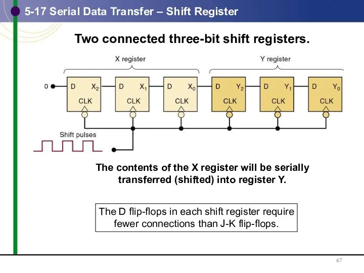
- 67. 5-17 Serial Data Transfer – Shift Register Two connected three-bit shift registers. The contents of the
- 68. 5-17 Serial Data Transfer – Shift Register Two connected three-bit shift registers. The complete transfer of
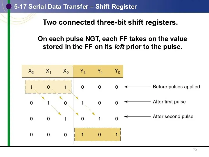
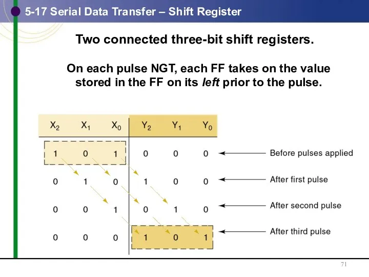
- 69. 5-17 Serial Data Transfer – Shift Register Two connected three-bit shift registers. On each pulse NGT,
- 70. 5-17 Serial Data Transfer – Shift Register Two connected three-bit shift registers. On each pulse NGT,
- 71. 5-17 Serial Data Transfer – Shift Register Two connected three-bit shift registers. On each pulse NGT,
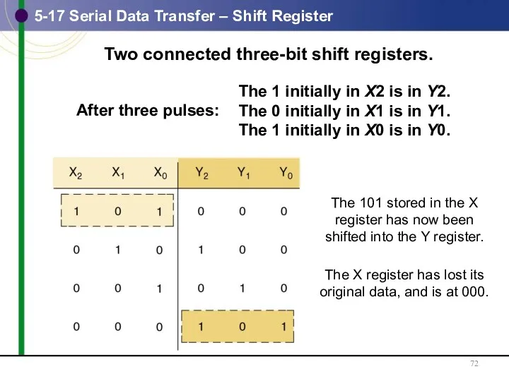
- 72. 5-17 Serial Data Transfer – Shift Register Two connected three-bit shift registers. The 101 stored in
- 73. 5-17 Serial Data Transfer vs. Parallel FFs can just as easily be connected so that information
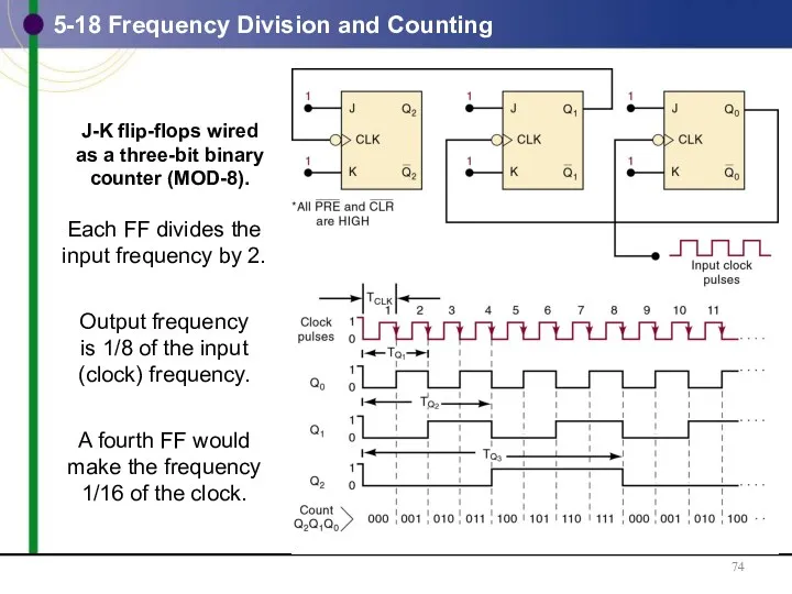
- 74. 5-18 Frequency Division and Counting J-K flip-flops wired as a three-bit binary counter (MOD-8). Each FF
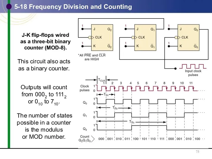
- 75. 5-18 Frequency Division and Counting J-K flip-flops wired as a three-bit binary counter (MOD-8). This circuit
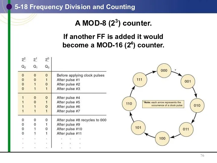
- 76. 5-18 Frequency Division and Counting A MOD-8 (23) counter. If another FF is added it would
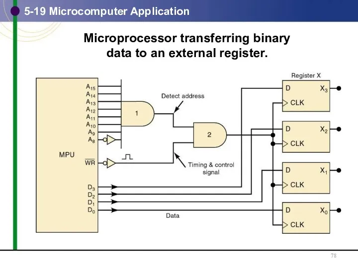
- 77. 5-19 Microcomputer Application Microprocessor units (MPUs) perform many functions involving use of registers for data transfer
- 78. 5-19 Microcomputer Application Microprocessor transferring binary data to an external register.
- 79. 5-20 Schmitt-Trigger Devices Not classified as a FF—but has a useful memory characteristic in certain situations.
- 80. 5-20 Schmitt-Trigger Devices Standard inverter response to slow noisy input.
- 81. 5-20 Schmitt-Trigger Devices Schmitt-trigger response to slow noisy input.
- 82. One shots are called monostable multivibrators because they have only one stable state. Prone to triggering
- 83. Nonretriggerable devices trigger & return to stable. Retriggerable devices can be triggered while in the quasi-stable
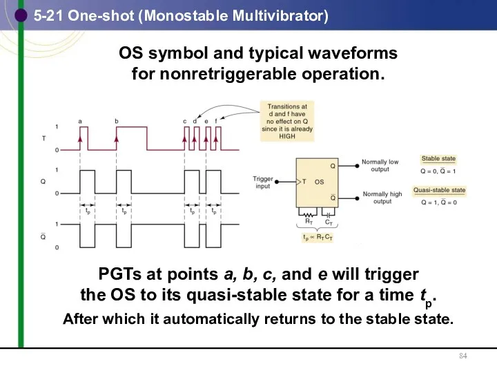
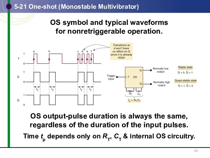
- 84. 5-21 One-shot (Monostable Multivibrator) OS symbol and typical waveforms for nonretriggerable operation. PGTs at points a,
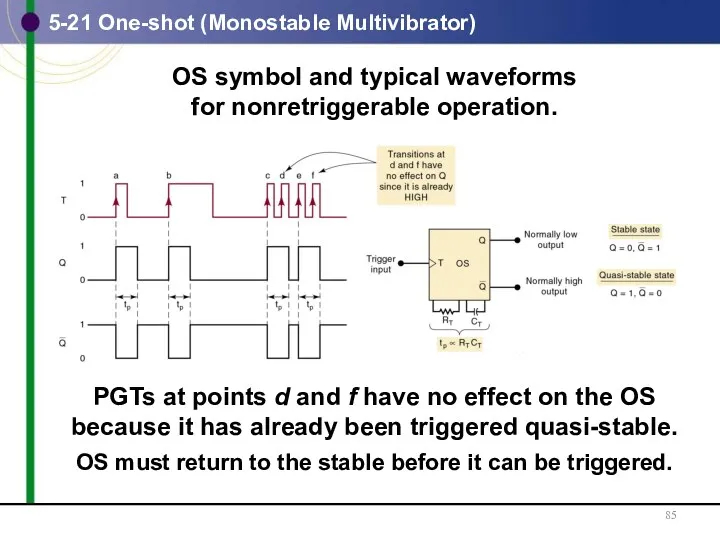
- 85. 5-21 One-shot (Monostable Multivibrator) OS symbol and typical waveforms for nonretriggerable operation. PGTs at points d
- 86. 5-21 One-shot (Monostable Multivibrator) OS symbol and typical waveforms for nonretriggerable operation. OS output-pulse duration is
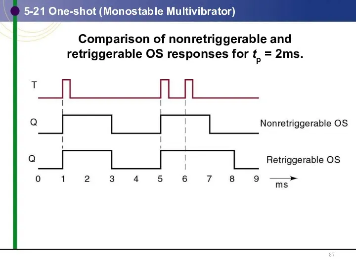
- 87. Comparison of nonretriggerable and retriggerable OS responses for tp = 2ms. 5-21 One-shot (Monostable Multivibrator)
- 88. Retriggerable OS begins a new tp interval each time it receives a trigger pulse. 5-21 One-shot
- 89. 74121 nonretriggerable one-shot IC. 5-21 One-shot (Monostable Multivibrator) Contains internal logic gates to allow inputs A1
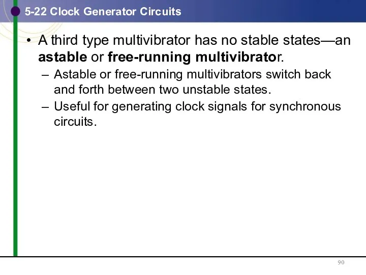
- 90. 5-22 Clock Generator Circuits A third type multivibrator has no stable states—an astable or free-running multivibrator.
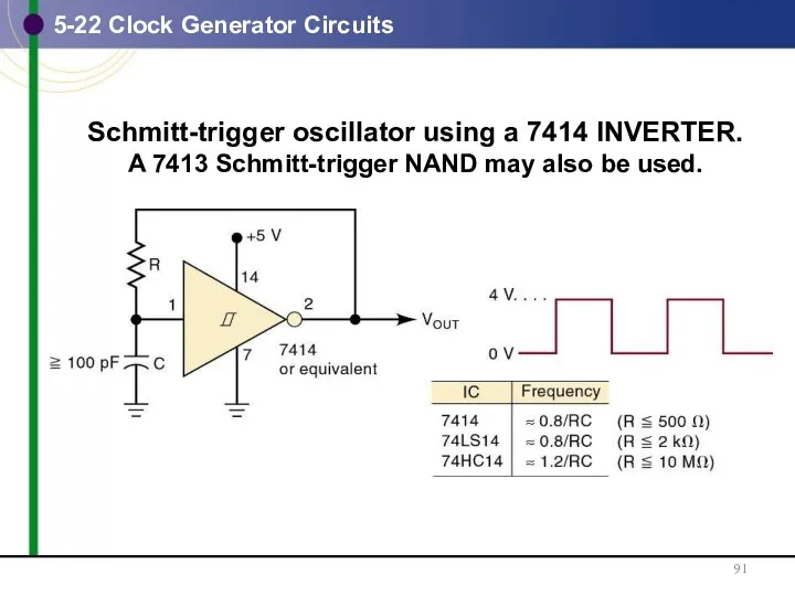
- 91. 5-22 Clock Generator Circuits Schmitt-trigger oscillator using a 7414 INVERTER. A 7413 Schmitt-trigger NAND may also
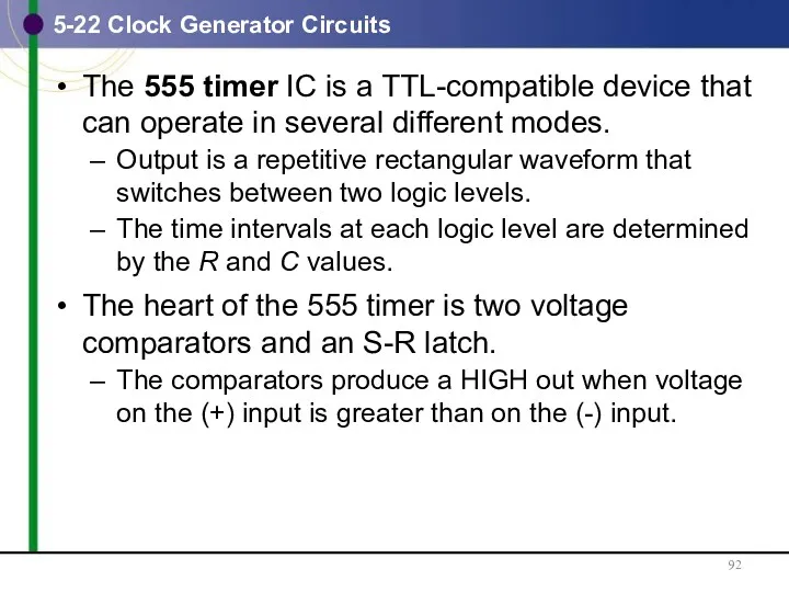
- 92. 5-22 Clock Generator Circuits The 555 timer IC is a TTL-compatible device that can operate in
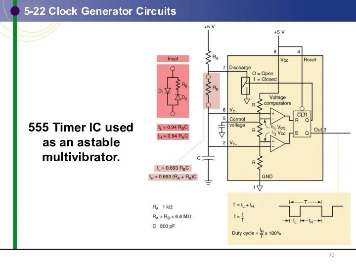
- 93. 5-22 Clock Generator Circuits 555 Timer IC used as an astable multivibrator.
- 94. 5-22 Clock Generator Circuits Crystal control may be used if a very stable clock is needed—used
- 95. 5-23 Troubleshooting Flip-Flop Circuits FFs are subject to the same faults that occur in combinational logic
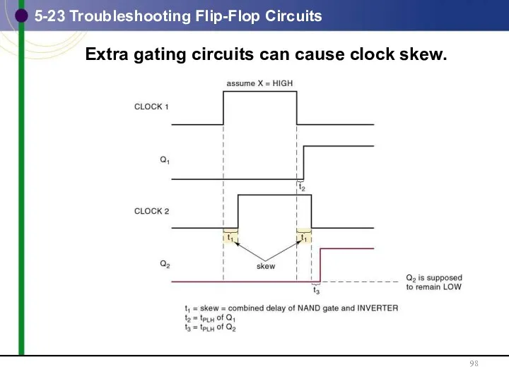
- 96. 5-23 Troubleshooting Flip-Flop Circuits Clock skew occurs when CLK signals arrive at different FFs at different
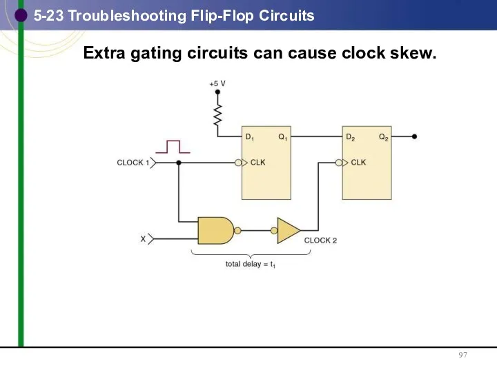
- 97. 5-23 Troubleshooting Flip-Flop Circuits Extra gating circuits can cause clock skew.
- 98. 5-23 Troubleshooting Flip-Flop Circuits Extra gating circuits can cause clock skew.
- 100. Скачать презентацию
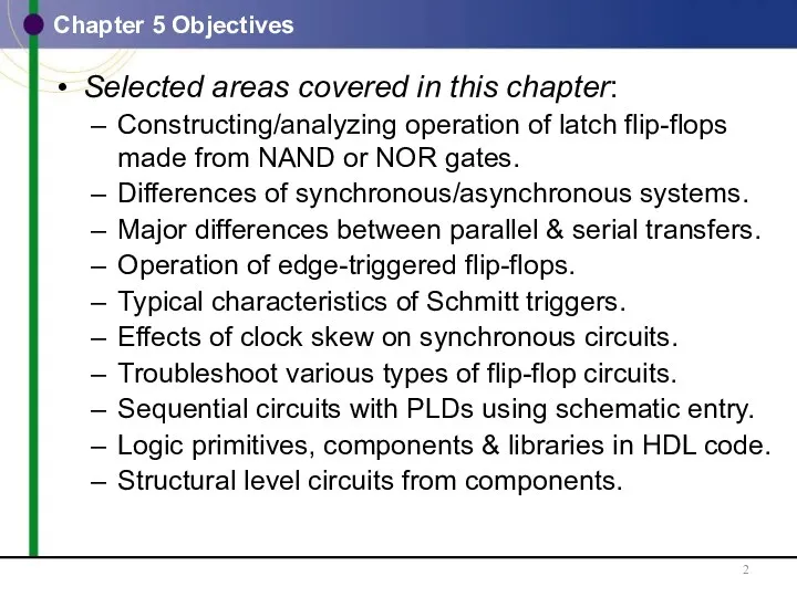
Selected areas covered in this chapter:
Constructing/analyzing operation of latch flip-flops made
Selected areas covered in this chapter:
Constructing/analyzing operation of latch flip-flops made
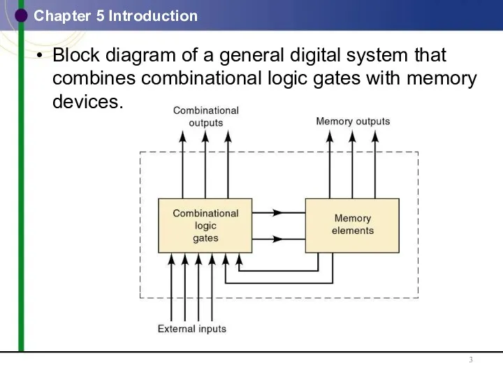
Chapter 5 Introduction
Block diagram of a general digital system that combines
Chapter 5 Introduction
Block diagram of a general digital system that combines
Chapter 5 Introduction
The most important memory element is the flip-flop (FF)—made
Chapter 5 Introduction
The most important memory element is the flip-flop (FF)—made
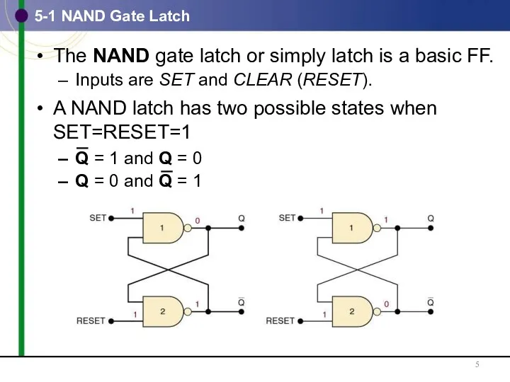
5-1 NAND Gate Latch
The NAND gate latch or simply latch is
5-1 NAND Gate Latch
The NAND gate latch or simply latch is
5-1 NAND Gate Latch – Setting the Latch (FF)
Pulsing the SET
5-1 NAND Gate Latch – Setting the Latch (FF)
Pulsing the SET
5-1 NAND Gate Latch – Resetting the Latch (FF)
Pulsing RESET LOW
5-1 NAND Gate Latch – Resetting the Latch (FF)
Pulsing RESET LOW
5-1 NAND Gate Latch – Alternate Representations
5-1 NAND Gate Latch – Alternate Representations
Summary of the NAND latch:
SET = 1, RESET = 1—Normal resting
Summary of the NAND latch:
SET = 1, RESET = 1—Normal resting
5-2 NOR Gate Latch
5-2 NOR Gate Latch
5-2 NOR Gate Latch - Summary
Summary of the NOR latch:
SET =
5-2 NOR Gate Latch - Summary
Summary of the NOR latch:
SET =
Example
Assume that Q=0 initially, and determine the Q waveform for the
Example
Assume that Q=0 initially, and determine the Q waveform for the
5-2 Power-Up
When power is applied, it is not possible to predict
5-2 Power-Up
When power is applied, it is not possible to predict
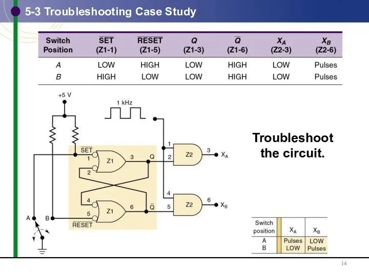
5-3 Troubleshooting Case Study
Troubleshoot
the circuit.
5-3 Troubleshooting Case Study
Troubleshoot
the circuit.
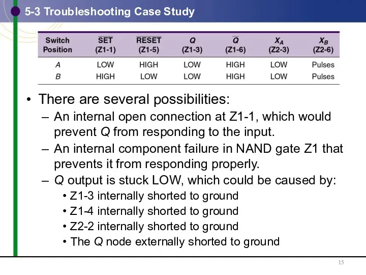
5-3 Troubleshooting Case Study
There are several possibilities:
An internal open connection at
5-3 Troubleshooting Case Study
There are several possibilities:
An internal open connection at
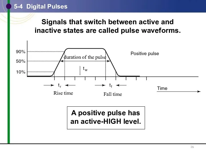
5-4 Digital Pulses
Signals that switch between active and
inactive states are called
5-4 Digital Pulses
Signals that switch between active and inactive states are called
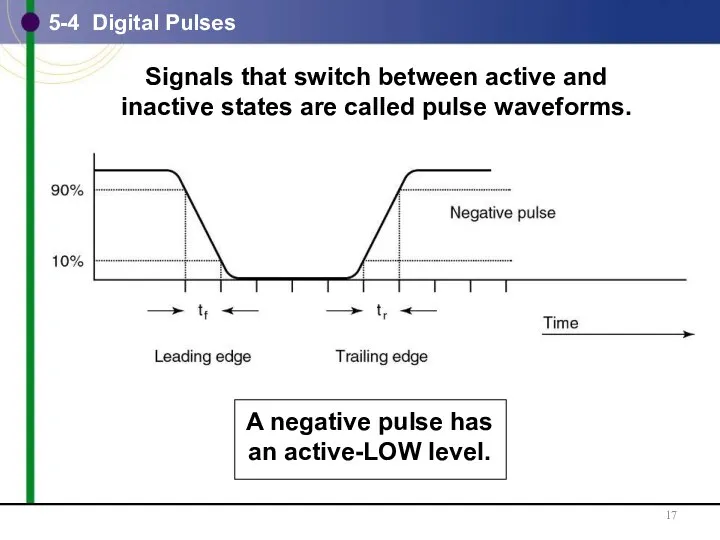
5-4 Digital Pulses
Signals that switch between active and
inactive states are called
5-4 Digital Pulses
Signals that switch between active and inactive states are called
5-4 Digital Pulses
In actual circuits it takes time for a pulse
5-4 Digital Pulses
In actual circuits it takes time for a pulse
5-4 Digital Pulses
In actual circuits it takes time for a pulse
5-4 Digital Pulses
In actual circuits it takes time for a pulse
5-4 Digital Pulses
In actual circuits it takes time for a pulse
5-4 Digital Pulses
In actual circuits it takes time for a pulse
5-5 Clock Signals and Clocked Flip-Flops
Digital systems can operate either asynchronously
5-5 Clock Signals and Clocked Flip-Flops
Digital systems can operate either asynchronously
5-5 Clock Signals and Clocked Flip-Flops
The clock signal is a rectangular
5-5 Clock Signals and Clocked Flip-Flops
The clock signal is a rectangular
5-5 Clock Signals and Clocked Flip-Flops
Clocked FFs change state on one
5-5 Clock Signals and Clocked Flip-Flops
Clocked FFs change state on one
5-5 Clock Signals and Clocked Flip-Flops
Control inputs have an effect on
5-5 Clock Signals and Clocked Flip-Flops
Control inputs have an effect on
5-5 Clock Signals and Clocked Flip-Flops
Setup time (tS) is the minimum
5-5 Clock Signals and Clocked Flip-Flops
Setup time (tS) is the minimum
5-5 Clock Signals and Clocked Flip-Flops
Hold time (tH) is the time
5-5 Clock Signals and Clocked Flip-Flops
Hold time (tH) is the time
5-6 Clocked S-R Flip-Flop
The S and R inputs are synchronous control
5-6 Clocked S-R Flip-Flop
The S and R inputs are synchronous control
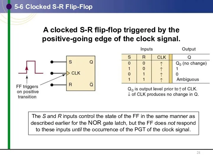
5-6 Clocked S-R Flip-Flop
A clocked S-R flip-flop triggered by the
positive-going edge
5-6 Clocked S-R Flip-Flop
A clocked S-R flip-flop triggered by the positive-going edge
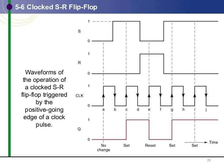
5-6 Clocked S-R Flip-Flop
Waveforms of
the operation of
a clocked S-R
flip-flop triggered by
5-6 Clocked S-R Flip-Flop
Waveforms of the operation of a clocked S-R flip-flop triggered by
5-6 Clocked S-R Flip-Flop
A clocked S-R flip-flop triggered by the
negative-going edge
5-6 Clocked S-R Flip-Flop
A clocked S-R flip-flop triggered by the negative-going edge
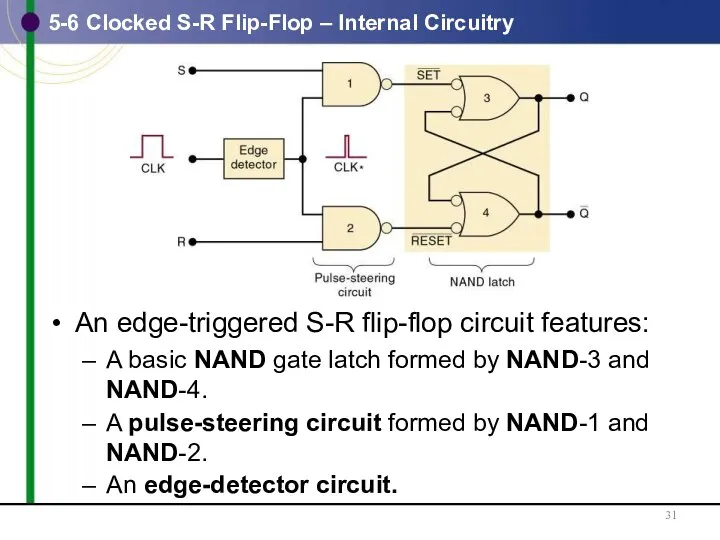
5-6 Clocked S-R Flip-Flop – Internal Circuitry
An edge-triggered S-R flip-flop circuit
5-6 Clocked S-R Flip-Flop – Internal Circuitry
An edge-triggered S-R flip-flop circuit
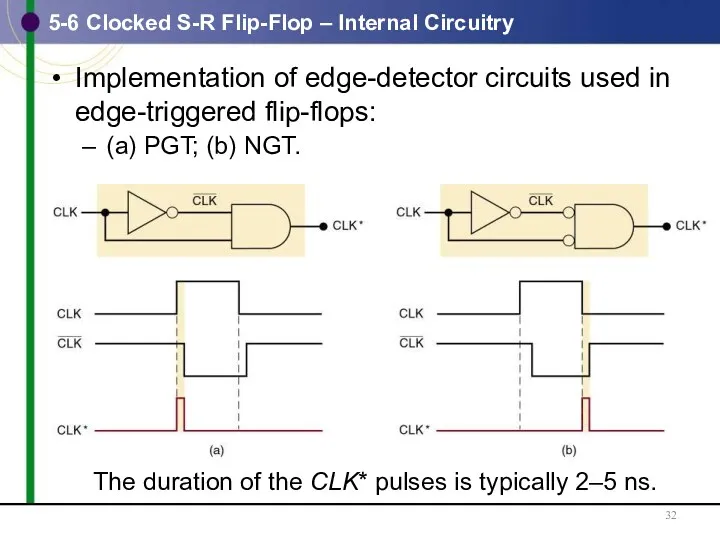
5-6 Clocked S-R Flip-Flop – Internal Circuitry
Implementation of edge-detector circuits used
5-6 Clocked S-R Flip-Flop – Internal Circuitry
Implementation of edge-detector circuits used
5-7 Clocked J-K Flip-Flop
Operates like the S-R FF.
J is SET, K
5-7 Clocked J-K Flip-Flop
Operates like the S-R FF.
J is SET, K
5-7 Clocked J-K Flip-Flop
Clocked J-K flip-flop that responds
only to the positive
5-7 Clocked J-K Flip-Flop
Clocked J-K flip-flop that responds only to the positive
5-7 Clocked J-K Flip-Flop
Clocked J-K flip-flop that responds
only to the negative
5-7 Clocked J-K Flip-Flop
Clocked J-K flip-flop that responds only to the negative
5-7 Clocked J-K Flip-Flop – Internal Circuitry
The internal circuitry of an
5-7 Clocked J-K Flip-Flop – Internal Circuitry
The internal circuitry of an
5-8 Clocked D Flip-Flop
One data input—output changes to the value of
5-8 Clocked D Flip-Flop
One data input—output changes to the value of
5-8 Clocked D Flip-Flop
D flip-flop that triggers only on
positive-going transitions.
5-8 Clocked D Flip-Flop
D flip-flop that triggers only on
positive-going transitions.
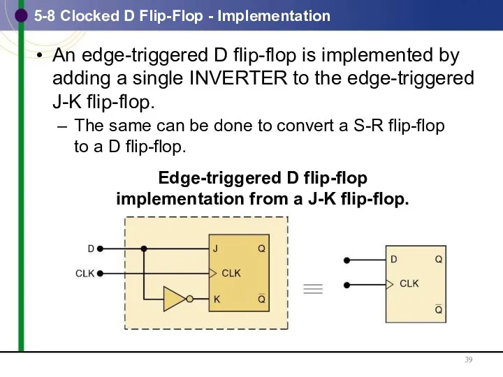
5-8 Clocked D Flip-Flop - Implementation
An edge-triggered D flip-flop is implemented
5-8 Clocked D Flip-Flop - Implementation
An edge-triggered D flip-flop is implemented
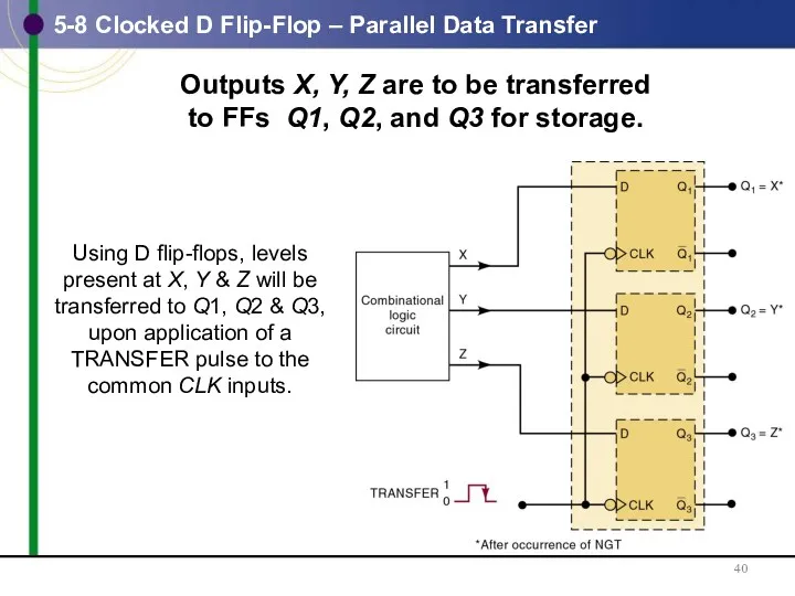
5-8 Clocked D Flip-Flop – Parallel Data Transfer
Outputs X, Y, Z
5-8 Clocked D Flip-Flop – Parallel Data Transfer
Outputs X, Y, Z
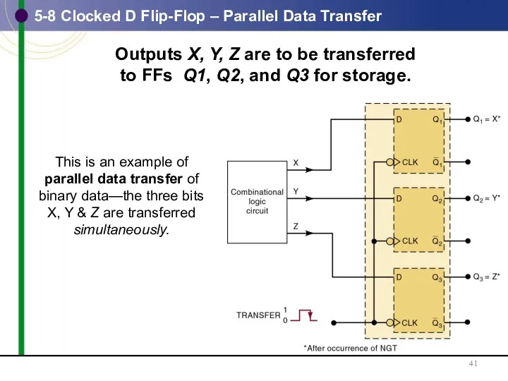
5-8 Clocked D Flip-Flop – Parallel Data Transfer
Outputs X, Y, Z
5-8 Clocked D Flip-Flop – Parallel Data Transfer
Outputs X, Y, Z
5-9 D Latch (Transparent Latch)
The edge-triggered D flip-flop uses an edge-detector
5-9 D Latch (Transparent Latch)
The edge-triggered D flip-flop uses an edge-detector
5-9 D Latch (Transparent Latch)
D latch structure, function table, logic symbol.
5-9 D Latch (Transparent Latch)
D latch structure, function table, logic symbol.
5-9 D Latch (Transparent Latch)
The circuit contains the NAND latch and
5-9 D Latch (Transparent Latch)
The circuit contains the NAND latch and
5-10 Asynchronous Inputs
Inputs that depend on the clock are synchronous.
Most clocked
5-10 Asynchronous Inputs
Inputs that depend on the clock are synchronous.
Most clocked
5-10 Asynchronous Inputs
Clocked J-K flip-flop with asynchronous inputs.
5-10 Asynchronous Inputs
Clocked J-K flip-flop with asynchronous inputs.
5-10 Asynchronous Inputs - Designations
IC manufacturers do not agree on nomenclature
5-10 Asynchronous Inputs - Designations
IC manufacturers do not agree on nomenclature
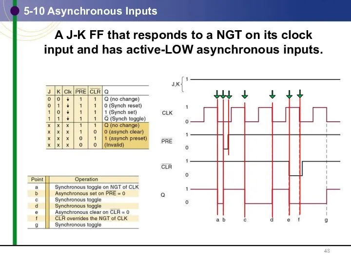
5-10 Asynchronous Inputs
A J-K FF that responds to a NGT on
5-10 Asynchronous Inputs
A J-K FF that responds to a NGT on
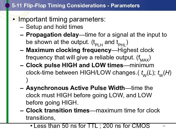
5-11 Flip-Flop Timing Considerations - Parameters
Important timing parameters:
Setup and hold times
Propagation
5-11 Flip-Flop Timing Considerations - Parameters
Important timing parameters:
Setup and hold times
Propagation
5-11 Flip-Flop Timing Considerations - Parameters
FF propagation delays.
Clock Pulse HIGH and
5-11 Flip-Flop Timing Considerations - Parameters
FF propagation delays.
Clock Pulse HIGH and
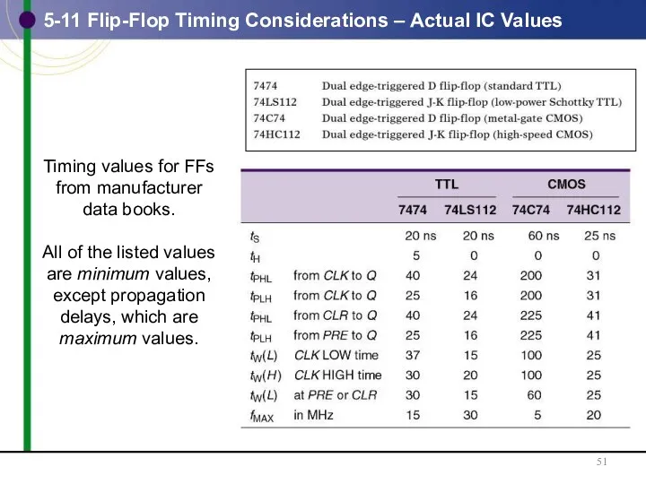
5-11 Flip-Flop Timing Considerations – Actual IC Values
5-11 Flip-Flop Timing Considerations – Actual IC Values
Example
From the table in the previous page:
Assume that Q=0. How long
Example
From the table in the previous page:
Assume that Q=0. How long
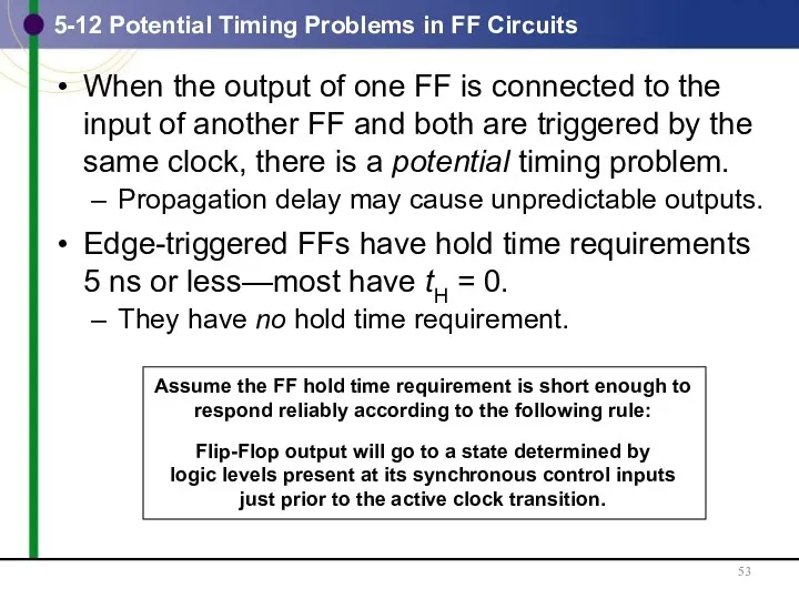
5-12 Potential Timing Problems in FF Circuits
When the output of one
5-12 Potential Timing Problems in FF Circuits
When the output of one
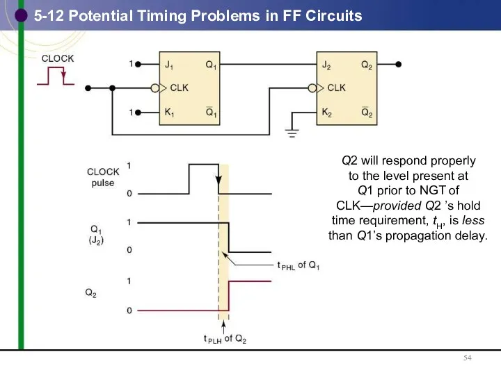
5-12 Potential Timing Problems in FF Circuits
5-12 Potential Timing Problems in FF Circuits
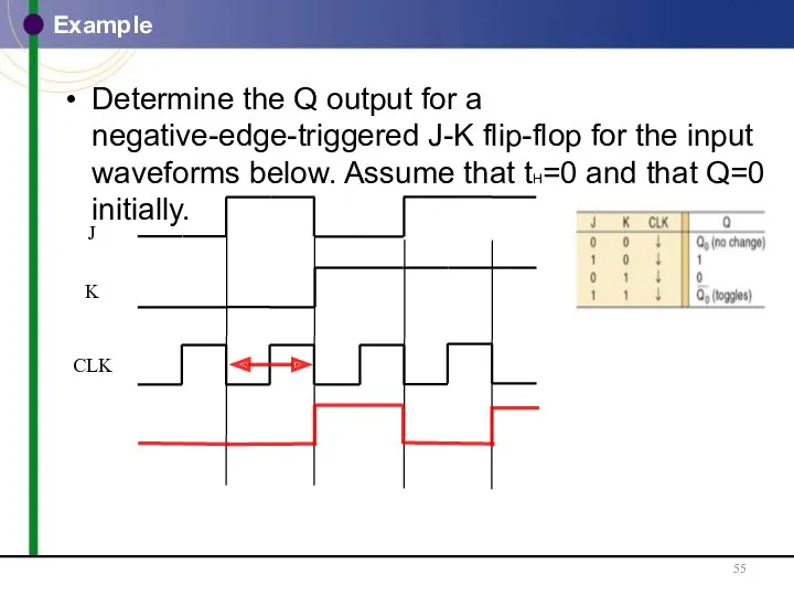
Example
Determine the Q output for a negative-edge-triggered J-K flip-flop for the
Example
Determine the Q output for a negative-edge-triggered J-K flip-flop for the
5-13 Flip-Flop Applications
Examples of applications:
Counting; Storing binary data
Transferring binary data between
5-13 Flip-Flop Applications
Examples of applications:
Counting; Storing binary data
Transferring binary data between
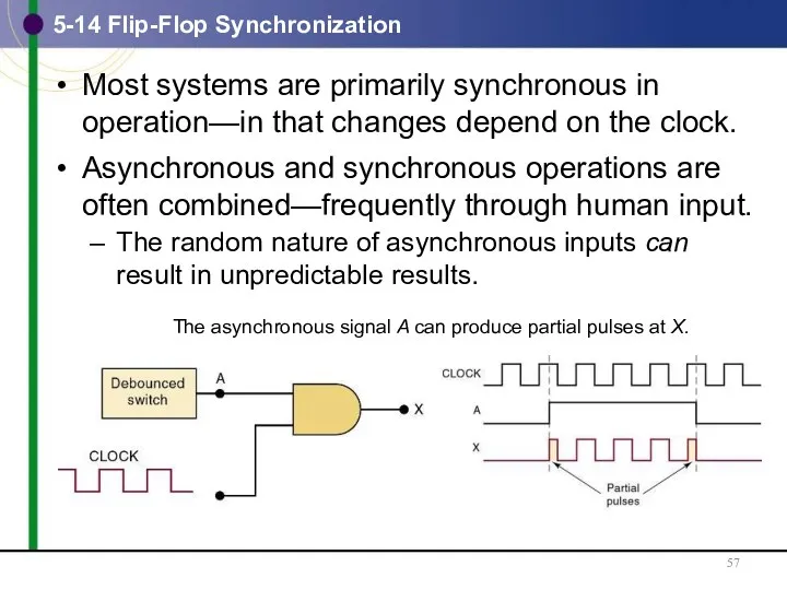
5-14 Flip-Flop Synchronization
Most systems are primarily synchronous in operation—in that changes
5-14 Flip-Flop Synchronization
Most systems are primarily synchronous in operation—in that changes
5-14 Flip-Flop Synchronization
An edge-triggered D flip-flop synchronizes the enabling of the
5-14 Flip-Flop Synchronization
An edge-triggered D flip-flop synchronizes the enabling of the
5-15 Detecting an Input Sequence
FFs provide features pure combinational logic gates
5-15 Detecting an Input Sequence
FFs provide features pure combinational logic gates
5-16 Data Storage and Transfer
FFs are commonly used for storage and
5-16 Data Storage and Transfer
FFs are commonly used for storage and
5-16 Data Storage and Transfer – Synchronous
5-16 Data Storage and Transfer – Synchronous
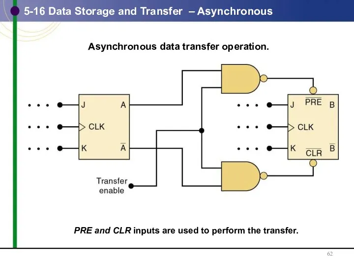
5-16 Data Storage and Transfer – Asynchronous
5-16 Data Storage and Transfer – Asynchronous
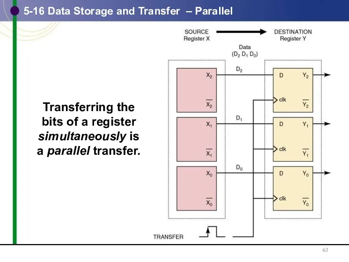
5-16 Data Storage and Transfer – Parallel
Transferring the bits of a
5-16 Data Storage and Transfer – Parallel
Transferring the bits of a
5-17 Serial Data Transfer
Transferring the bits of a register a bit
5-17 Serial Data Transfer
Transferring the bits of a register a bit
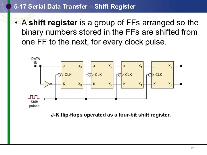
5-17 Serial Data Transfer – Shift Register
A shift register is a
5-17 Serial Data Transfer – Shift Register
A shift register is a
5-17 Serial Data Transfer – Shift Register
Input data are shifted
left to
5-17 Serial Data Transfer – Shift Register
Input data are shifted left to
5-17 Serial Data Transfer – Shift Register
Two connected three-bit shift registers.
The
5-17 Serial Data Transfer – Shift Register
Two connected three-bit shift registers.
The
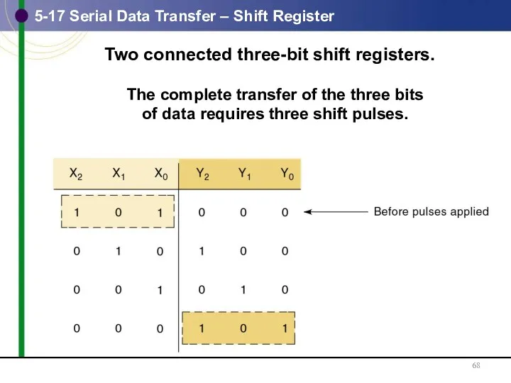
5-17 Serial Data Transfer – Shift Register
Two connected three-bit shift registers.
The
5-17 Serial Data Transfer – Shift Register
Two connected three-bit shift registers.
The
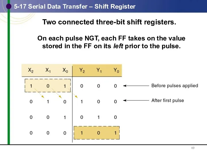
5-17 Serial Data Transfer – Shift Register
Two connected three-bit shift registers.
On
5-17 Serial Data Transfer – Shift Register
Two connected three-bit shift registers.
On
5-17 Serial Data Transfer – Shift Register
Two connected three-bit shift registers.
On
5-17 Serial Data Transfer – Shift Register
Two connected three-bit shift registers.
On
5-17 Serial Data Transfer – Shift Register
Two connected three-bit shift registers.
On
5-17 Serial Data Transfer – Shift Register
Two connected three-bit shift registers.
On
5-17 Serial Data Transfer – Shift Register
Two connected three-bit shift registers.
The
5-17 Serial Data Transfer – Shift Register
Two connected three-bit shift registers.
The
5-17 Serial Data Transfer vs. Parallel
FFs can just as easily be
5-17 Serial Data Transfer vs. Parallel
FFs can just as easily be
5-18 Frequency Division and Counting
J-K flip-flops wired
as a three-bit binary
counter (MOD-8).
Each
5-18 Frequency Division and Counting
J-K flip-flops wired
as a three-bit binary
counter (MOD-8).
Each
5-18 Frequency Division and Counting
J-K flip-flops wired
as a three-bit binary
counter (MOD-8).
This
5-18 Frequency Division and Counting
J-K flip-flops wired
as a three-bit binary
counter (MOD-8).
This
5-18 Frequency Division and Counting
A MOD-8 (23) counter.
If another FF
5-18 Frequency Division and Counting
A MOD-8 (23) counter.
If another FF
5-19 Microcomputer Application
Microprocessor units (MPUs) perform many functions involving use of
5-19 Microcomputer Application
Microprocessor units (MPUs) perform many functions involving use of
5-19 Microcomputer Application
Microprocessor transferring binary
data to an external register.
5-19 Microcomputer Application
Microprocessor transferring binary
data to an external register.
5-20 Schmitt-Trigger Devices
Not classified as a FF—but has a useful memory
5-20 Schmitt-Trigger Devices
Not classified as a FF—but has a useful memory
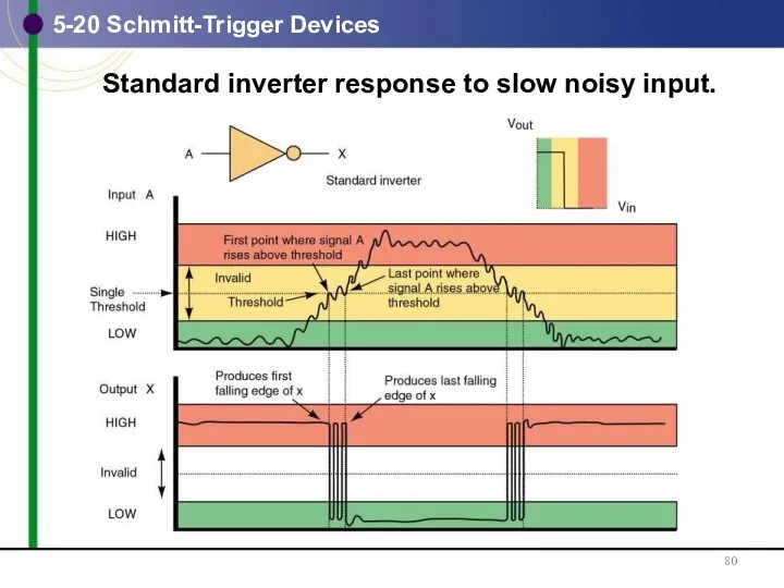
5-20 Schmitt-Trigger Devices
Standard inverter response to slow noisy input.
5-20 Schmitt-Trigger Devices
Standard inverter response to slow noisy input.
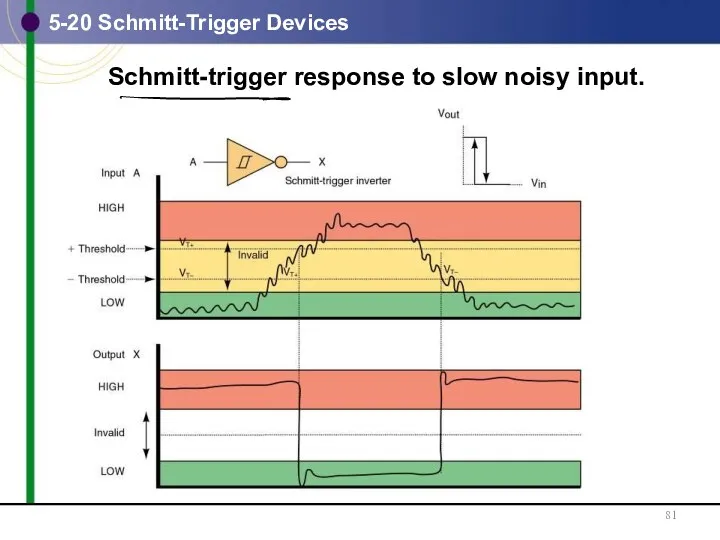
5-20 Schmitt-Trigger Devices
Schmitt-trigger response to slow noisy input.
5-20 Schmitt-Trigger Devices
Schmitt-trigger response to slow noisy input.
One shots are called monostable multivibrators because they have only one
One shots are called monostable multivibrators because they have only one
Nonretriggerable devices trigger & return to stable.
Retriggerable devices can be triggered
Nonretriggerable devices trigger & return to stable.
Retriggerable devices can be triggered
5-21 One-shot (Monostable Multivibrator)
OS symbol and typical waveforms
for nonretriggerable operation.
PGTs at
5-21 One-shot (Monostable Multivibrator)
OS symbol and typical waveforms
for nonretriggerable operation.
PGTs at
5-21 One-shot (Monostable Multivibrator)
OS symbol and typical waveforms
for nonretriggerable operation.
PGTs at
5-21 One-shot (Monostable Multivibrator)
OS symbol and typical waveforms
for nonretriggerable operation.
PGTs at
5-21 One-shot (Monostable Multivibrator)
OS symbol and typical waveforms
for nonretriggerable operation.
OS output-pulse
5-21 One-shot (Monostable Multivibrator)
OS symbol and typical waveforms
for nonretriggerable operation.
OS output-pulse
Comparison of nonretriggerable and
retriggerable OS responses for tp = 2ms.
5-21
Comparison of nonretriggerable and
retriggerable OS responses for tp = 2ms.
5-21
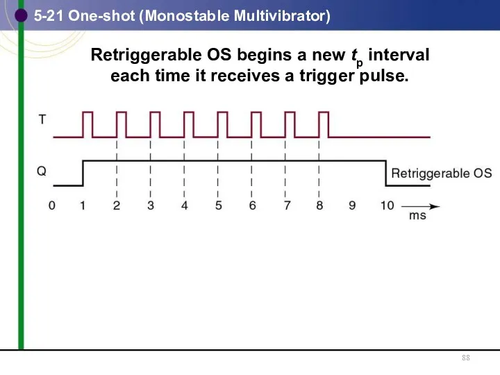
Retriggerable OS begins a new tp interval
each time it receives a
Retriggerable OS begins a new tp interval each time it receives a
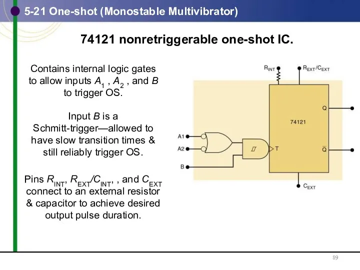
74121 nonretriggerable one-shot IC.
5-21 One-shot (Monostable Multivibrator)
Contains internal logic gates
to
74121 nonretriggerable one-shot IC.
5-21 One-shot (Monostable Multivibrator)
Contains internal logic gates to
5-22 Clock Generator Circuits
A third type multivibrator has no stable states—an
5-22 Clock Generator Circuits
A third type multivibrator has no stable states—an
5-22 Clock Generator Circuits
Schmitt-trigger oscillator using a 7414 INVERTER.
A 7413 Schmitt-trigger
5-22 Clock Generator Circuits
Schmitt-trigger oscillator using a 7414 INVERTER. A 7413 Schmitt-trigger
5-22 Clock Generator Circuits
The 555 timer IC is a TTL-compatible device
5-22 Clock Generator Circuits
The 555 timer IC is a TTL-compatible device
5-22 Clock Generator Circuits
555 Timer IC used as an astable multivibrator.
5-22 Clock Generator Circuits
555 Timer IC used as an astable multivibrator.
5-22 Clock Generator Circuits
Crystal control may be used if a very
5-22 Clock Generator Circuits
Crystal control may be used if a very
5-23 Troubleshooting Flip-Flop Circuits
FFs are subject to the same faults that
5-23 Troubleshooting Flip-Flop Circuits
FFs are subject to the same faults that
5-23 Troubleshooting Flip-Flop Circuits
Clock skew occurs when CLK signals arrive
at different
5-23 Troubleshooting Flip-Flop Circuits
Clock skew occurs when CLK signals arrive at different
5-23 Troubleshooting Flip-Flop Circuits
Extra gating circuits can cause clock skew.
5-23 Troubleshooting Flip-Flop Circuits
Extra gating circuits can cause clock skew.
5-23 Troubleshooting Flip-Flop Circuits
Extra gating circuits can cause clock skew.
5-23 Troubleshooting Flip-Flop Circuits
Extra gating circuits can cause clock skew.
 День Великомучениці Катерини
 Проект Ани и Саши
 В весеннем лесу (объёмная аппликация)
 Кореновский молочно-консервный комбинат
 Презентация для родителей Поход в музей.
 sravneniya
 презентация предметно-пространственной среды группы
 Гальванические покрытия
 Законы сохранения импульса и механической энергии,
 презентация на тему:Город, в котором я живу
 Казахстан в годы Великой Отечественной войны 22 июня 1941- 9 мая 1945
 Тьютерский проект Оказание методической и консультативной помощи ОУ по внедрению инклюзивного образования
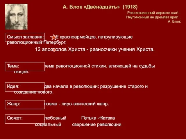 А. Блок, поэма Двенадцать (1918)
 Development 3 Group Lab 1 (VD)
 юбилей Вовы
 Технология строительства тоннелей горным способом в породах крепких и средней крепости
 Студенттердің тамақтану ерекшелігі мен ұйымдастырылуын бағалау. Ғылыми жоба
 Библиотеки Вконтакте
 Высокомолекулярные соединения полимеры
 Урок мужества!
 Елена Александровна Благинина
 Инструменты распознования текстов и компьютерного перевода. Обработка текстовой информации
 Презентация Насекомые
 Блеск и сила здоровых волос с точки зрения химии
 SIMATIC RTU 3030C – самодостаточное и автономное
 Арамсояу (лат. Cuscuta)
 Догляд за хворими з хірургічними захворюваннями і ушкодженнями органів сечостатевої системи
 Роль художественной литературы в речевом развитии детей