- HW Repair Guide SM-G7102 ( Galaxy Grand 2)

Содержание
- 2. All functionality, features, specifications and other product information provided in this document including, but not limited
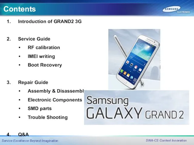
- 3. Contents Introduction of GRAND2 3G Service Guide RF calibration IMEI writing Boot Recovery Repair Guide Assembly
- 4. Introduction of GRAND2 3G (1/3) Specification
- 5. Introduction of GRAND2 3G (2/3) Features Optimal Wide View Satisfying Viewing Experience Maximize Every Inch 1.
- 6. Introduction of GRAND2 3G (3/3) Galaxy Grand Galaxy Grand2 Category
- 7. RF calibration (1/2) ★ For GRAND2(SM-G7102), new IF cable should be used for IMEI writing and
- 8. RF calibration (2/2) 2. Run Calibration program
- 9. IMEI Writing (1/4) ★ For GRAND2 3G(SM-G7102), new IF cable should be used for IMEI writing
- 10. IMEI Writing (2/4) 2) Select MODE as ‘Service’, Model folder as ‘SM-G7102’,check IMEI option and click
- 11. IMEI Writing (3/4) 4) Click ‘Hardware Config’ option. 5) Click ‘Port Setting’ in the phone option,
- 12. IMEI Writing (4/4) 7) Enter IMEI number and click ‘Apply’ button. 8) Click ‘Model Info’ button
- 13. Boot Recovery Emergency download mode & Odin T-Flash mode
- 14. Brief Process Preparing SD card, using working GRNAD2 3G (Samsung Method) Inserting the SD Card to
- 15. EDL mode verification Device not booting up Confirming a device is in Emergency Download mode (eDL
- 16. Insert External SD Card to normal phone to copy Boot loader to SD card Go to
- 17. Use the SD card to recover a device going to eDL mode. Plug in the SD
- 18. Flash the Latest Pit and Boot loader on to the device ( as shown below )
- 19. Now remove the SD Card from Faulty device. Go to download mode (Vol Dn + Home
- 20. Disassembly & Assembly Instruction Disassembly & Assembly Instruction
- 21. Disassemble Instruction 1) Disassemble LCD connector protect cover. ※ Caution 1) Be careful of scratch and
- 22. 3) Displace the temperature chamber for 10 minute Detach the TSP/LCD Assay using Vaccum jig ※
- 23. 4) Unscrew the 10 points. ※ Caution 1) Be careful of scratch and molding damage. Disassemble
- 24. 5) Detach the PBA/Sheildcan Assay. ※ Caution 1) Be careful of damage to the EARJACK Module.
- 25. 6) Disassemble the RCV, Sensor, SPK from PBA. Unscrew the 2 points. ※ Caution 1) Be
- 26. 7) Separate the VGA, MEGA Camera from PBA Array. ※ Caution 1) Be careful of damage
- 27. 8) Separate the Top dummy, Bottom dummy & Speaker from hook. ※ Caution 1) Be careful
- 28. 1) Assemble the Top dummy, Speaker on shield can. ※ Caution 1) Be careful of damage
- 29. 2) Assemble the PBA on Shieldcan. Screw the 2 points.. ※ Caution 1) Be careful of
- 30. 3) Assemble PBA assay to the Rear Assemble Bottom dummy on the Rear ※ Caution 1)
- 31. 4) Remove the TSP tape (in case of replacing the new TSP module) ※ Caution 1)
- 32. 6) Screw the 10 points of the Rear. 1.2 ± 0.1 Kgf/㎠. ※ Caution 1) Be
- 33. 7) Attach the LCD assay to the Rear Assay. 8) Assemble LCD connector. ※ Caution 1)
- 34. 9) Assemble LCD connector protect cover. ※ Caution 1) Be careful of scratch and molding damage.
- 35. 10) Press the set using pressure jig. ※ Caution 1) - Pressure : 5~6 kgf/cm2 -
- 36. Electronic Components Electronic Components
- 37. Electronic Components (1/2) SPK Module Ear Jack SIM card socket + Micro SD card socket Shield
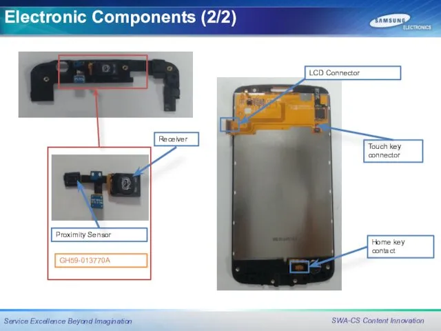
- 38. Touch key connector Proximity Sensor LCD Connector GH59-013770A Home key contact Receiver Electronic Components (2/2)
- 39. SMD parts (TOP side) U202 1009-001058 HALL IC U401 1203-008057 PMIC U602 1203-004776 Motor LDO OSC200
- 40. SMD parts (Bottom side) LED600 0601-003364 Flash LED HDC601 3711-007467 Connector(1.9M CAM) U200 1201-003631 GPS LNA(Low
- 41. Troubleshooting Troubleshooting
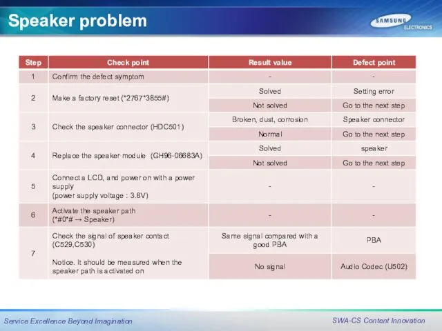
- 42. Power problem
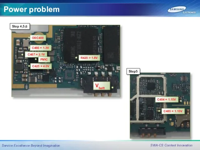
- 43. Power problem C466 = 1.3V Step 4,5,6 C467 = 2.1V OSC400 Vbatt C425 = 4.0V C485
- 44. RF (GSM,WCDMA)
- 45. RF (GSM,WCDMA)
- 46. RF (GSM,WCDMA)
- 47. RF (GSM,WCDMA)
- 48. BT/WIFI
- 49. BT/WIFI
- 50. BT/WIFI
- 51. GPS/GLONASS
- 52. Step1 GPS/GLONASS
- 53. GPS ANTENNA contact Step2 GPS/GLONASS
- 54. GPS/GLONASS Step4,5 ANT200 C226 C226 F202 C234 L205 U200[LNA] C245 C230 C241
- 55. GPS/GLONASS Step4,5,6 GPS IC(U102) C156
- 56. Speaker problem
- 57. Step3 connector HDC501 Speaker connector Step4 SPK Module Ear Jack GH96-06683A Speaker problem
- 58. Step7 C530 C529 U502 Audio Codec Sound signal path connector Speaker problem
- 59. Display Problem
- 60. Display problem Step6 Step6 C602 LCD power path from PMIC Step2,3,5,7 HDC600 C606 C605 R602 LCD(include
- 61. Touch problem
- 62. Touch problem C604 Step2 Step3 Step6,7 R601 R602 C433 U401 PMIC Step6 LCD(include TSP) CONNECTOR TSP
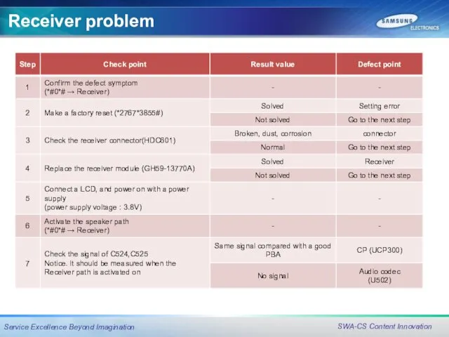
- 63. Receiver problem
- 64. Receiver problem Step3 Step4 Receiver connector Proximity Sensor GH59-13770A Receiver Step7 C525 C524 U502 Audio Codec
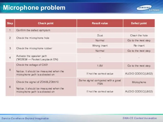
- 65. Microphone problem
- 66. Microphone problem Step2,3 Microphone Microphone Rubber Holder
- 67. SIM card detection problem
- 68. SIM card detection problem Step5 SIM600 [SIM card socket + Micro SD card socket] Step 2
- 70. Скачать презентацию
All functionality, features, specifications and other product information
provided in this document including, but not limited to, the benefits, design,
pricing, components, performance, availability, and capabilities of the product are
subject to change without notice or obligation. Samsung reserves the right to
make changes to this document and the product described herein, at anytime, with
out obligation
Contents
Introduction of GRAND2 3G
Service Guide
RF calibration
IMEI writing
Boot Recovery
Repair Guide
Assembly & Disassembly
Electronic
Contents
Introduction of GRAND2 3G
Service Guide
RF calibration
IMEI writing
Boot Recovery
Repair Guide
Assembly & Disassembly
Electronic
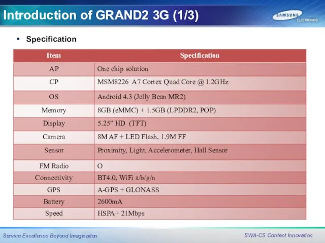
Introduction of GRAND2 3G (1/3)
Specification
Introduction of GRAND2 3G (1/3)
Specification
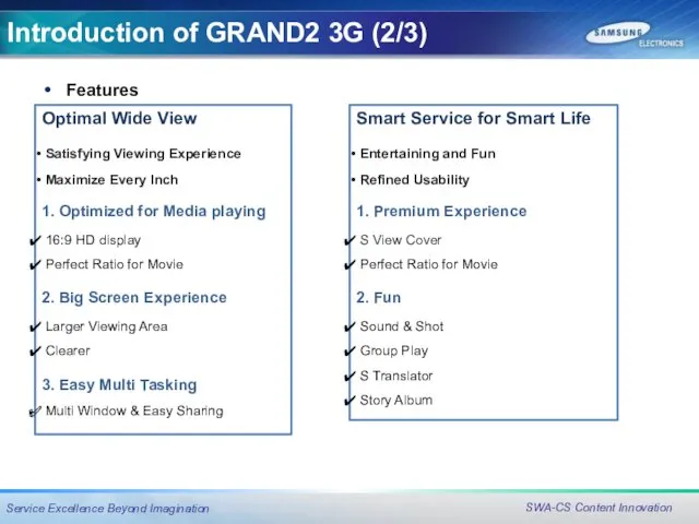
Introduction of GRAND2 3G (2/3)
Features
Optimal Wide View
Satisfying Viewing Experience
Maximize
Introduction of GRAND2 3G (2/3)
Features
Optimal Wide View
Satisfying Viewing Experience
Maximize
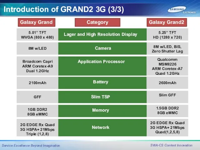
Introduction of GRAND2 3G (3/3)
Galaxy Grand
Galaxy Grand2
Category
Introduction of GRAND2 3G (3/3)
Galaxy Grand
Galaxy Grand2
Category
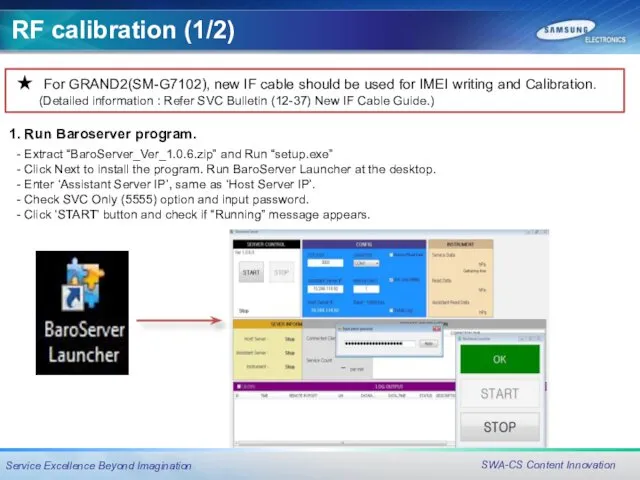
RF calibration (1/2)
★ For GRAND2(SM-G7102), new IF cable should be
RF calibration (1/2)
★ For GRAND2(SM-G7102), new IF cable should be
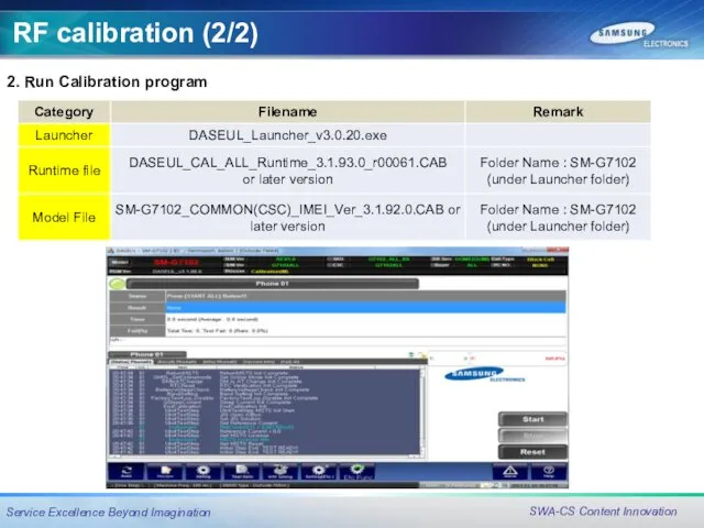
RF calibration (2/2)
2. Run Calibration program
RF calibration (2/2)
2. Run Calibration program
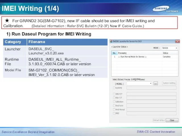
IMEI Writing (1/4)
★ For GRAND2 3G(SM-G7102), new IF cable should
IMEI Writing (1/4)
★ For GRAND2 3G(SM-G7102), new IF cable should
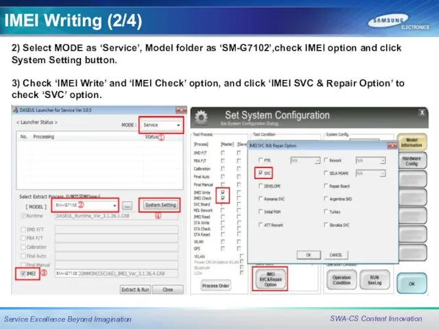
IMEI Writing (2/4)
2) Select MODE as ‘Service’, Model folder as ‘SM-G7102’,check
IMEI Writing (2/4)
2) Select MODE as ‘Service’, Model folder as ‘SM-G7102’,check
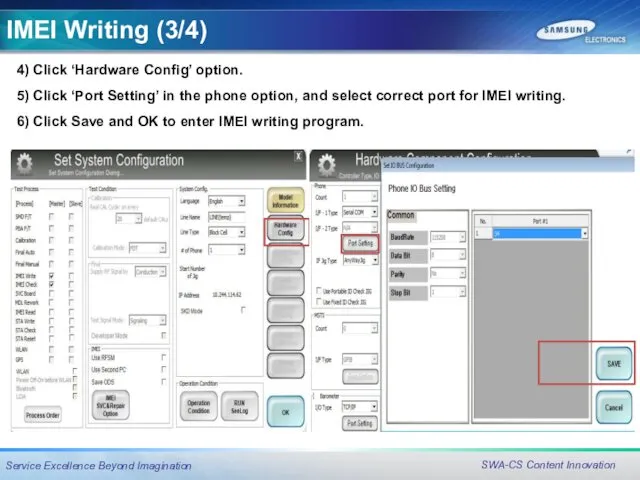
IMEI Writing (3/4)
4) Click ‘Hardware Config’ option.
5) Click ‘Port Setting’
IMEI Writing (3/4)
4) Click ‘Hardware Config’ option.
5) Click ‘Port Setting’
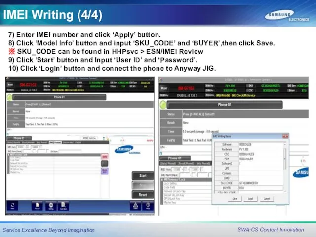
IMEI Writing (4/4)
7) Enter IMEI number and click ‘Apply’ button.
8)
IMEI Writing (4/4)
7) Enter IMEI number and click ‘Apply’ button.
8)
Boot Recovery
Emergency download mode & Odin T-Flash mode
Boot Recovery
Emergency download mode & Odin T-Flash mode
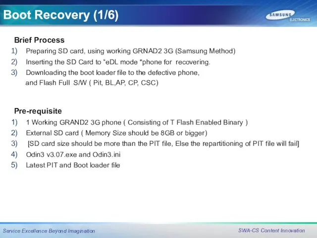
Brief Process
Preparing SD card, using working GRNAD2 3G (Samsung Method)
Inserting the
Brief Process
Preparing SD card, using working GRNAD2 3G (Samsung Method)
Inserting the
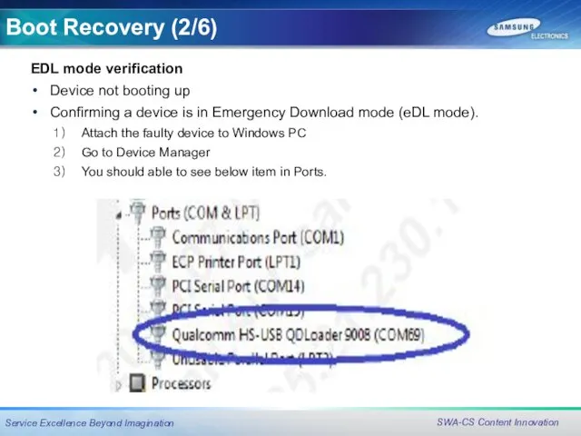
EDL mode verification
Device not booting up
Confirming a device is in Emergency
EDL mode verification
Device not booting up
Confirming a device is in Emergency
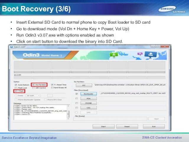
Insert External SD Card to normal phone to copy Boot loader
Insert External SD Card to normal phone to copy Boot loader
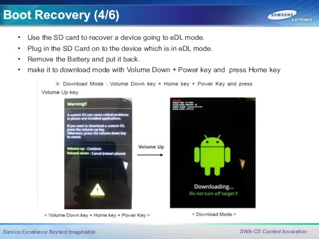
Use the SD card to recover a device going to eDL
Use the SD card to recover a device going to eDL
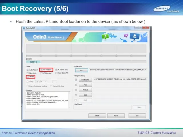
Flash the Latest Pit and Boot loader on to the device
Flash the Latest Pit and Boot loader on to the device
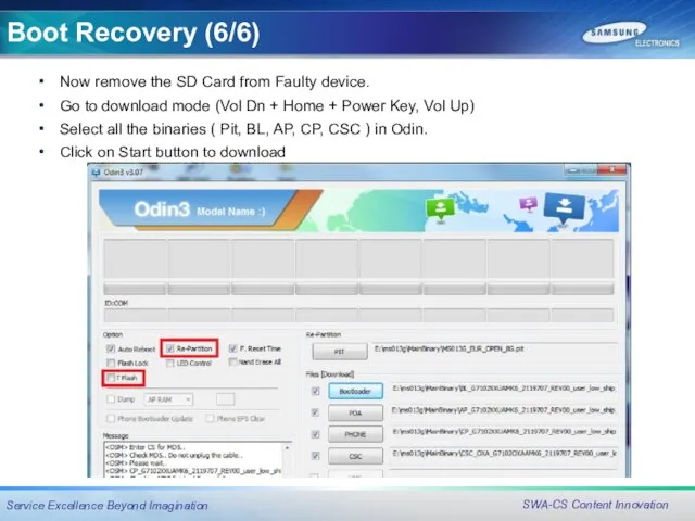
Now remove the SD Card from Faulty device.
Go to download mode
Now remove the SD Card from Faulty device.
Go to download mode
Disassembly & Assembly Instruction
Disassembly & Assembly
Instruction
Disassembly & Assembly Instruction
Disassembly & Assembly
Instruction
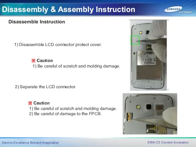
Disassemble Instruction
1) Disassemble LCD connector protect cover.
※ Caution
1) Be careful of scratch
Disassemble Instruction
1) Disassemble LCD connector protect cover.
※ Caution
1) Be careful of scratch
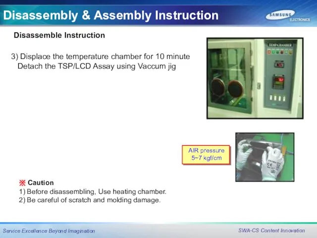
3) Displace the temperature chamber for 10 minute
Detach the TSP/LCD
3) Displace the temperature chamber for 10 minute
Detach the TSP/LCD
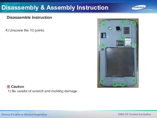
4) Unscrew the 10 points.
※ Caution
1) Be careful of scratch
4) Unscrew the 10 points.
※ Caution
1) Be careful of scratch
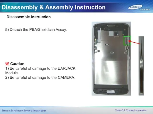
5) Detach the PBA/Sheildcan Assay.
※ Caution
1) Be careful of damage to
5) Detach the PBA/Sheildcan Assay.
※ Caution
1) Be careful of damage to
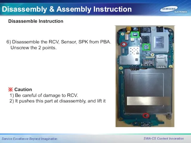
6) Disassemble the RCV, Sensor, SPK from PBA.
Unscrew the 2
6) Disassemble the RCV, Sensor, SPK from PBA.
Unscrew the 2
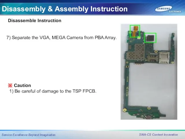
7) Separate the VGA, MEGA Camera from PBA Array.
※ Caution
1)
7) Separate the VGA, MEGA Camera from PBA Array.
※ Caution
1)
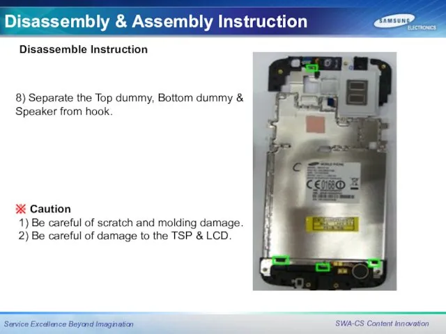
8) Separate the Top dummy, Bottom dummy & Speaker from hook.
※
8) Separate the Top dummy, Bottom dummy & Speaker from hook.
※
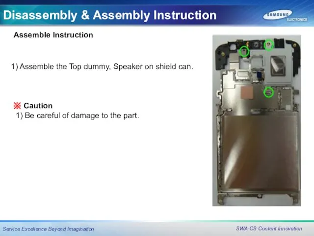
1) Assemble the Top dummy, Speaker on shield can.
※ Caution
1)
1) Assemble the Top dummy, Speaker on shield can.
※ Caution
1)
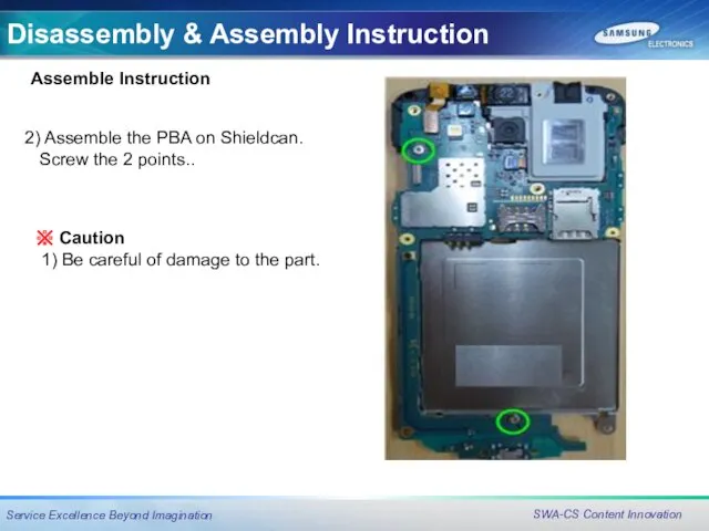
2) Assemble the PBA on Shieldcan.
Screw the 2 points..
※ Caution
2) Assemble the PBA on Shieldcan.
Screw the 2 points..
※ Caution
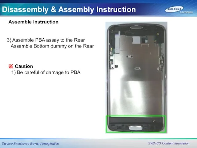
3) Assemble PBA assay to the Rear
Assemble Bottom dummy on
3) Assemble PBA assay to the Rear
Assemble Bottom dummy on
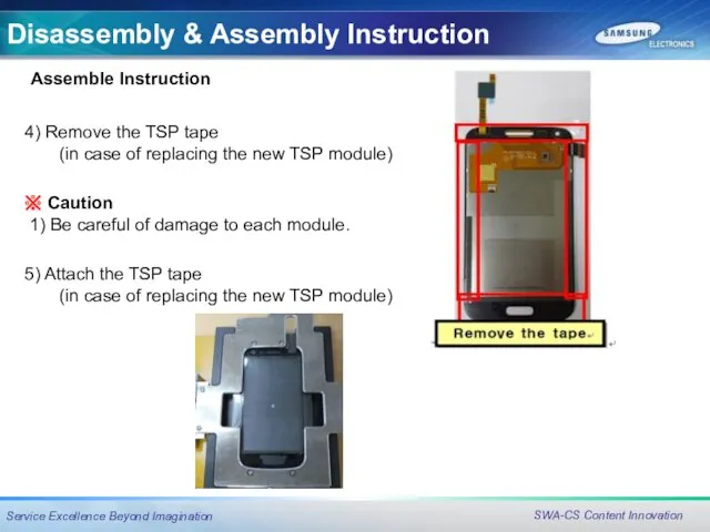
4) Remove the TSP tape
(in case of replacing the new
4) Remove the TSP tape
(in case of replacing the new
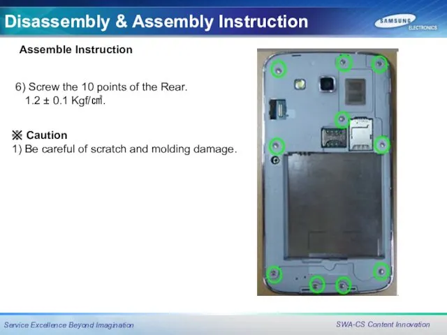
6) Screw the 10 points of the Rear.
1.2 ± 0.1
6) Screw the 10 points of the Rear.
1.2 ± 0.1
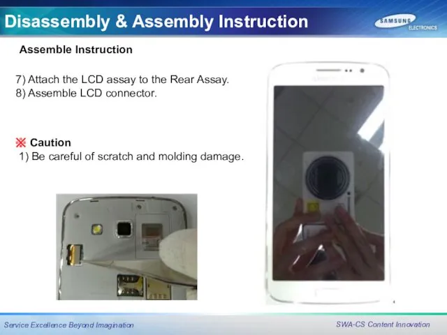
7) Attach the LCD assay to the Rear Assay.
8) Assemble LCD
7) Attach the LCD assay to the Rear Assay.
8) Assemble LCD
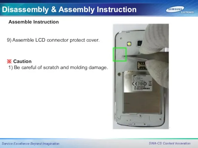
9) Assemble LCD connector protect cover.
※ Caution
1) Be careful of
9) Assemble LCD connector protect cover.
※ Caution
1) Be careful of
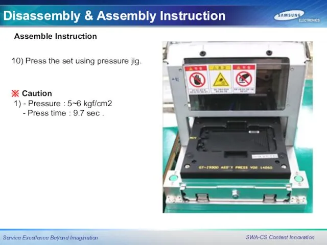
10) Press the set using pressure jig.
※ Caution
1) - Pressure
10) Press the set using pressure jig.
※ Caution
1) - Pressure
Electronic Components
Electronic
Components
Electronic Components
Electronic
Components
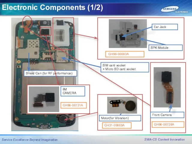
Electronic Components (1/2)
SPK Module
Ear Jack
SIM card socket
+ Micro SD card socket
Shield
Electronic Components (1/2)
SPK Module
Ear Jack
SIM card socket
+ Micro SD card socket
Shield
Touch key
connector
Proximity Sensor
LCD Connector
GH59-013770A
Home key
contact
Receiver
Electronic Components (2/2)
Touch key
connector
Proximity Sensor
LCD Connector
GH59-013770A
Home key
contact
Receiver
Electronic Components (2/2)
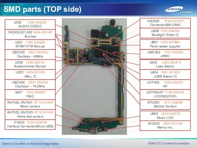
SMD parts (TOP side)
U202 1009-001058
HALL IC
U401 1203-008057
PMIC
U602 1203-004776
Motor LDO
OSC200 2801-005323
Oscillator
SMD parts (TOP side)
U202 1009-001058
HALL IC
U401 1203-008057
PMIC
U602 1203-004776
Motor LDO
OSC200 2801-005323
Oscillator
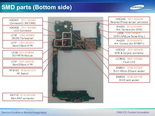
SMD parts (Bottom side)
LED600 0601-003364
Flash LED
HDC601 3711-007467
Connector(1.9M CAM)
U200 1201-003631
GPS LNA(Low Noise
SMD parts (Bottom side)
LED600 0601-003364
Flash LED
HDC601 3711-007467
Connector(1.9M CAM)
U200 1201-003631
GPS LNA(Low Noise
Troubleshooting
Troubleshooting
Troubleshooting
Troubleshooting
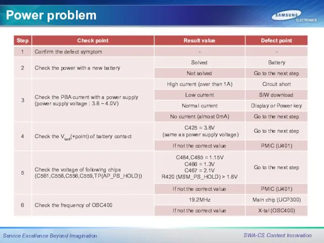
Power problem
Power problem
Power problem
C466 = 1.3V
Step 4,5,6
C467 = 2.1V
OSC400
Vbatt
C425 = 4.0V
C485 =
Power problem
C466 = 1.3V
Step 4,5,6
C467 = 2.1V
OSC400
Vbatt
C425 = 4.0V
C485 =
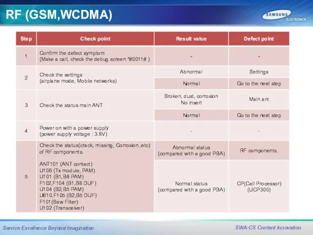
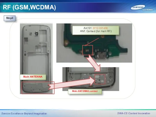
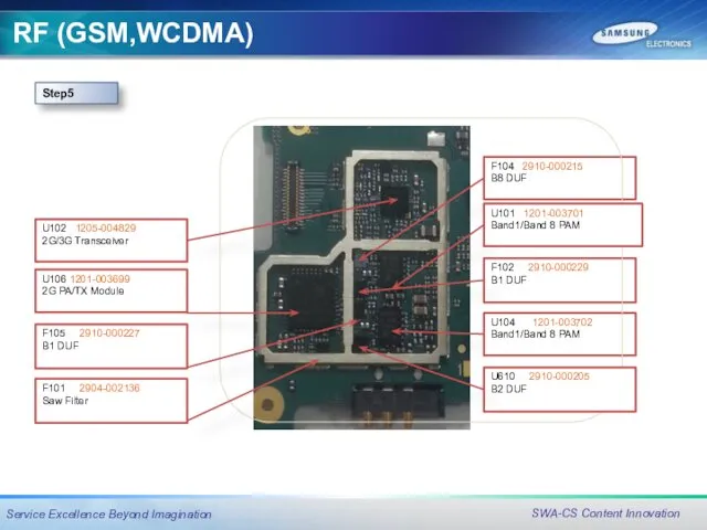
RF (GSM,WCDMA)
RF (GSM,WCDMA)
RF (GSM,WCDMA)
RF (GSM,WCDMA)
RF (GSM,WCDMA)
RF (GSM,WCDMA)
RF (GSM,WCDMA)
RF (GSM,WCDMA)
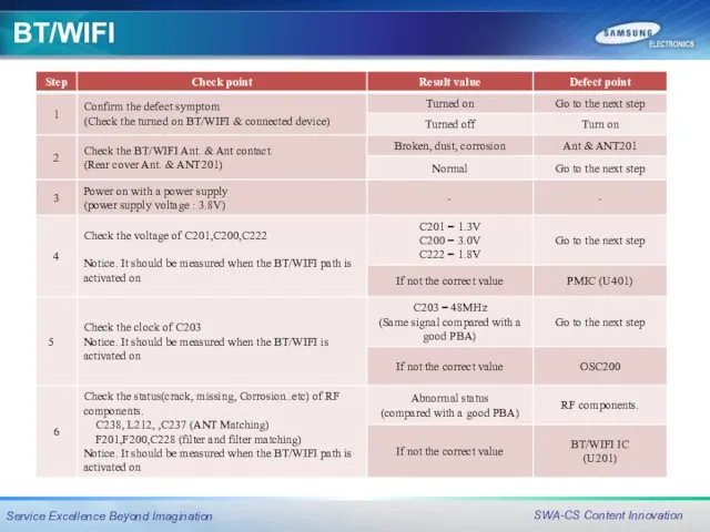
BT/WIFI
BT/WIFI
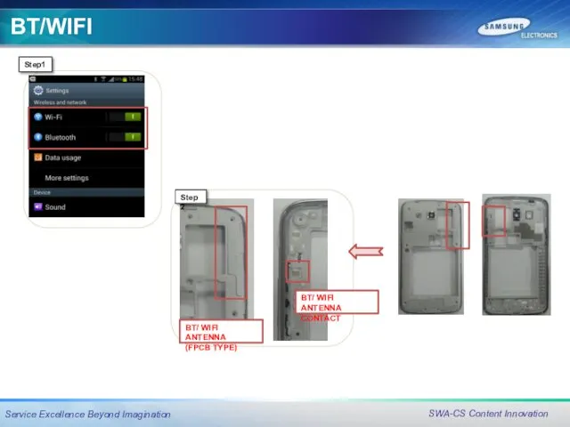
BT/WIFI
BT/WIFI
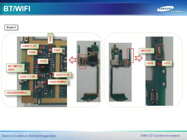
BT/WIFI
BT/WIFI
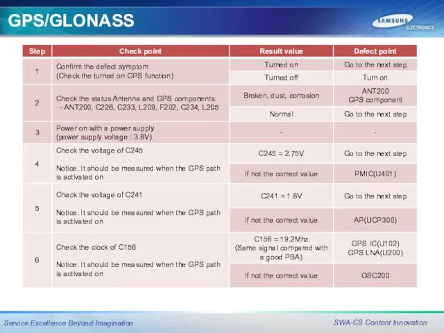
GPS/GLONASS
GPS/GLONASS
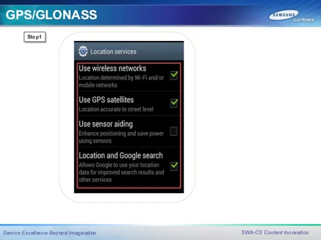
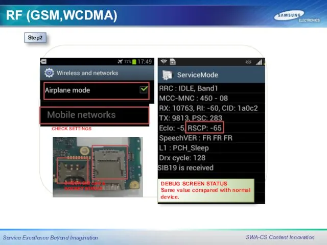
Step1
GPS/GLONASS
Step1
GPS/GLONASS
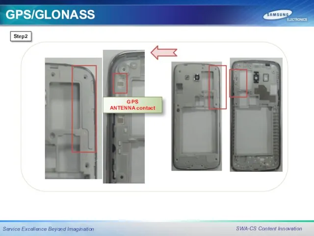
GPS
ANTENNA contact
Step2
GPS/GLONASS
GPS
ANTENNA contact
Step2
GPS/GLONASS
![GPS/GLONASS Step4,5 ANT200 C226 C226 F202 C234 L205 U200[LNA] C245 C230 C241](/_ipx/f_webp&q_80&fit_contain&s_1440x1080/imagesDir/jpg/20674/slide-53.jpg)
GPS/GLONASS
Step4,5
ANT200
C226
C226
F202
C234
L205
U200[LNA]
C245
C230
C241
GPS/GLONASS
Step4,5
ANT200
C226
C226
F202
C234
L205
U200[LNA]
C245
C230
C241
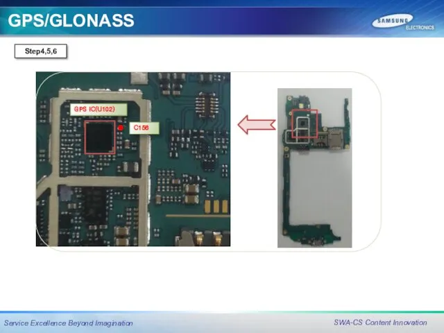
GPS/GLONASS
Step4,5,6
GPS IC(U102)
C156
GPS/GLONASS
Step4,5,6
GPS IC(U102)
C156
Speaker problem
Speaker problem
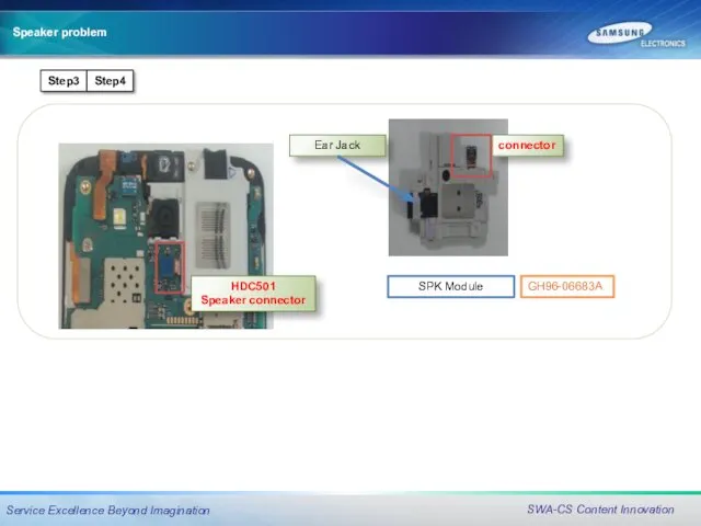
Step3
connector
HDC501
Speaker connector
Step4
SPK Module
Ear Jack
GH96-06683A
Speaker problem
Step3
connector
HDC501
Speaker connector
Step4
SPK Module
Ear Jack
GH96-06683A
Speaker problem
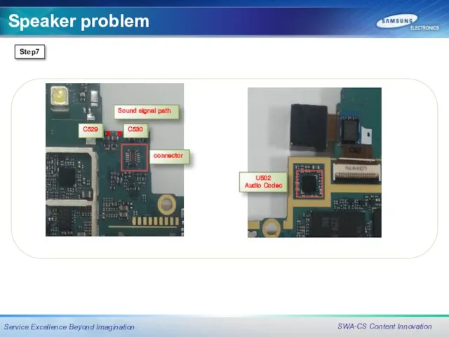
Step7
C530
C529
U502
Audio Codec
Sound signal path
connector
Speaker problem
Step7
C530
C529
U502
Audio Codec
Sound signal path
connector
Speaker problem
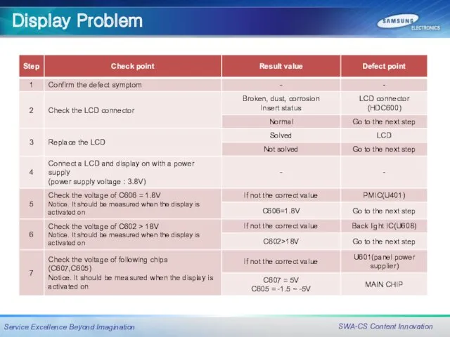
Display Problem
Display Problem
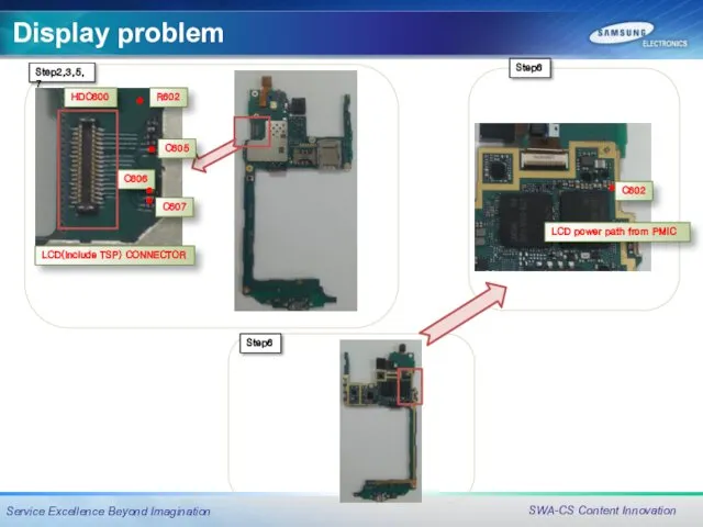
Display problem
Step6
Step6
C602
LCD power path from PMIC
Step2,3,5,7
HDC600
C606
C605
R602
LCD(include TSP) CONNECTOR
C607
Display problem
Step6
Step6
C602
LCD power path from PMIC
Step2,3,5,7
HDC600
C606
C605
R602
LCD(include TSP) CONNECTOR
C607
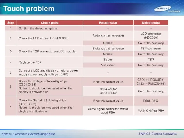
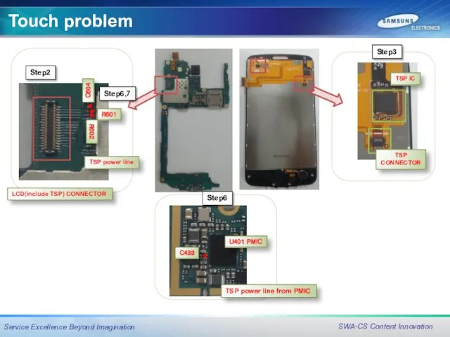
Touch problem
Touch problem
Touch problem
C604
Step2
Step3
Step6,7
R601
R602
C433
U401 PMIC
Step6
LCD(include TSP) CONNECTOR
TSP
CONNECTOR
TSP IC
TSP power line
TSP power line
Touch problem
C604
Step2
Step3
Step6,7
R601
R602
C433
U401 PMIC
Step6
LCD(include TSP) CONNECTOR
TSP
CONNECTOR
TSP IC
TSP power line
TSP power line
Receiver problem
Receiver problem
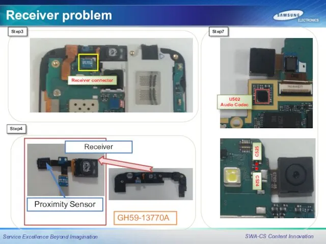
Receiver problem
Step3
Step4
Receiver connector
Proximity Sensor
GH59-13770A
Receiver
Step7
C525
C524
U502
Audio Codec
Receiver problem
Step3
Step4
Receiver connector
Proximity Sensor
GH59-13770A
Receiver
Step7
C525
C524
U502
Audio Codec
Microphone problem
Microphone problem
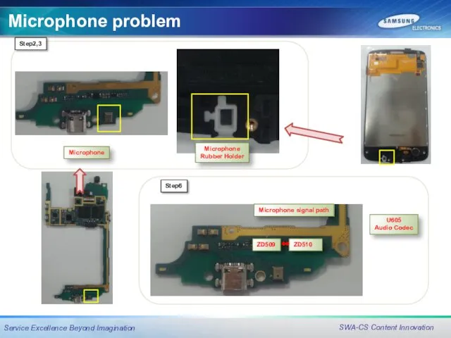
Microphone problem
Step2,3
Microphone
Microphone
Rubber Holder
Microphone problem
Step2,3
Microphone
Microphone
Rubber Holder
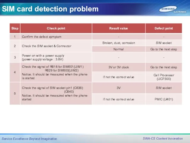
SIM card detection problem
SIM card detection problem
SIM card detection problem
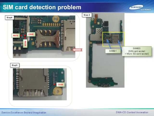
Step5
SIM600
[SIM card socket
+ Micro SD card socket]
Step 2
Step4
R629
C640
R618
SIM601
C636
SIM card detection problem
Step5
SIM600
[SIM card socket
+ Micro SD card socket]
Step 2
Step4
R629
C640
R618
SIM601
C636
 Революція на граніті
 Rice Cooker HD3033 df Technical Info. Product Features
 Выбор и подготовка материалов для резки
 Троянская война и поэмы Гомера
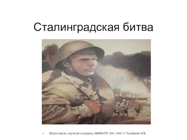 Stalingradskaya_bitva_02_02_22
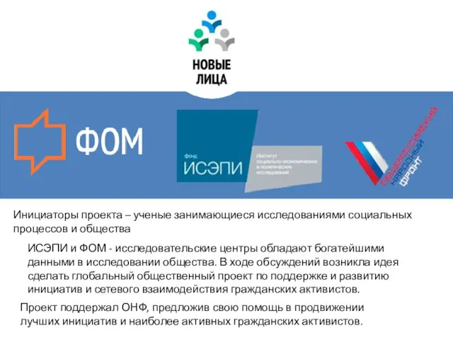 Новые лица
 Химия и живопись.
 Artificial Intelligence
 Эффективность применения программы Преобразование обучения для XXI века в работе педагога в адаптационный период обучающихся первых классов к школьному обучению
 Палех - город мастеров
 Технология ручной дуговой сварки
 Крупнейшие экологические катастрофы - презентация к конференции по географии Глобальные проблемы человечества
 Виды ислама
 Страны Востока в XVI – XVIII веках
 Приглашаем студентов на практику и трудоустройство. Акционерное общество Ижевский радиозавод
 Health is above wealth
 музыка в кино
 Подготовка к сочинению по картине И.Э.Грабаря Февральская лазурь
 Физические основы механики молекулярная физика. Основы термодинамики
 Презентация Воспоминания о Великой Отечественной Войне ветерана ВОВ Киселева Степана Павловича( в стихах его собственного сочинения).
 Массивы в языке Pascal. (Урок 42)
 Қазақстан Республикасында тілдердің қызметі мен дамуын қамтамасыздандырудағы әрекеттері
 Виды фундаментов. (Лекция 16)
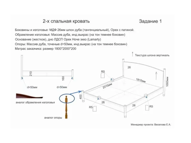 2-х спальная кровать
 Кариес зубов у детей. Лечение
 Türk EÄitim Tarihi 3
 Волонтёры Победы. Курск
 ФК Русичи-2008 г. Орёл