- Micro Fabrication Basics

Содержание
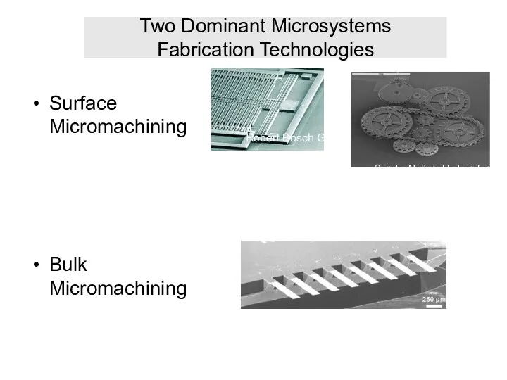
- 2. Two Dominant Microsystems Fabrication Technologies Surface Micromachining Bulk Micromachining Robert Bosch GmbH Sandia National Laboratories IBM
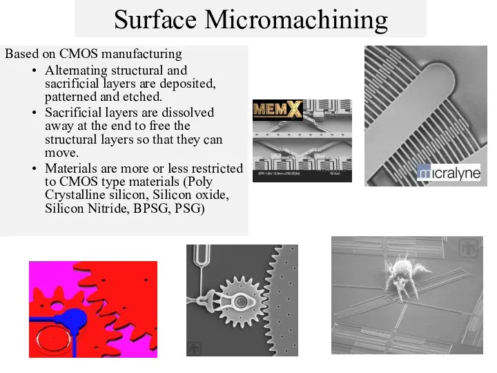
- 3. Surface Micromachining Based on CMOS manufacturing Alternating structural and sacrificial layers are deposited, patterned and etched.
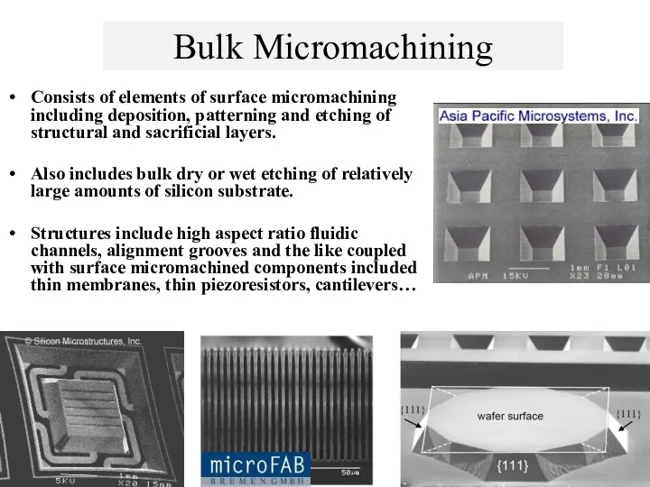
- 4. Bulk Micromachining Consists of elements of surface micromachining including deposition, patterning and etching of structural and
- 5. Surface Micromachining Materials Sacrificial Layers Silicon Dioxide Structural Layers Poly crystalline silicon (“Poly”) Insulators Silicon dioxide,
- 6. Surface Micromachining Process Outline Obtain Silicon Crystal Wafers Deposit (or grow) thin film material Pattern (Photo
- 7. Cross Sectional View
- 8. Surface Micromachining Process Start with a Silicon Crystal Substrate Slice and Polish to create wafers Ingot
- 9. Grow Thermal Oxide First layer acts as an insulator – it is a thermally grown silicon
- 10. MEMS deposition technology can be classified in two groups: Depositions that happen because of a chemical
- 11. Thermal oxidation Oxidation of the substrate surface in an oxygen rich atmosphere. The temperature is raised
- 12. Evaporation In evaporation the substrate is placed inside a vacuum chamber, in which a block (source)
- 13. Sputtering The substrate is placed in a vacuum chamber with the source material, named a target,
- 14. Casting In this process the material to be deposited is dissolved in liquid form in a
- 15. Basic Idea behind lithographic processing
- 16. Basic Idea behind lithographic processing
- 17. Essential Lithography Steps Coat wafer with photo resist Expose resist to a pattern Develop resist Bake
- 18. Lithographic Processing: Wafers
- 19. Film growth/deposition
- 20. Photoresist Spinning
- 21. Masking and Exposure
- 22. Developing the Pattern
- 23. Etch the Material
- 24. Repeat Process
- 25. Final Release
- 26. Pattern Transfer Lithography in the MEMS context is typically the transfer of a pattern to a
- 27. Resist When resist is exposed to a radiation source of a specific a wavelength, the chemical
- 29. Positive and negative resist
- 30. Positive Resist Chemistry
- 31. Molecular weight shift
- 32. Typical Positive Resist process EXAMPLE PROCESS: AZ5206 POSITIVE MASK PLATE Soak mask plate in acetone >
- 33. Negative Resist Cemistry
- 34. Typical Negative resist process EXAMPLE PROCESS: SAL NEGATIVE MASK PLATE Soak mask plate in acetone >
- 35. Lithography is the principal mechanism for pattern definition in micromachining. A photosensitive layer is often used
- 36. Alignment In order to make useful devices the patterns for different lithography steps that belong to
- 37. Depending on the lithography equipment used, the feature on the mask used for registration of the
- 38. Poor alignment mark design for a DRIE through the wafer etch (cross hair is released and
- 39. Exposure At the edges of pattern light is scattered and diffracted, so if an image is
- 40. The Lithography Module Dehydration bake - dehydrate the wafer to aid resist adhesion. HMDS prime -
- 41. Etching In order to form a functional MEMS structure on a substrate, it is necessary to
- 42. Wet etching Requires is a container with a liquid solution that will dissolve the material in
- 43. Dry Etching In RIE, the substrate is placed inside a reactor in which several gases are
- 44. Anisotropic vs Isotropic Etch
- 45. Wet (Isotropic) Etch
- 46. Dry (Anisotropic) Etch
- 47. Sputter etching is essentially RIE without reactive ions. The systems used are very similar in principle
- 48. Wafer Example Design Masks Silicon Substrate Deposit 5K Oxide Pattern Mask 1 Wet Etch (Timed BOE)
- 49. The Masks (Design) Mask 1 Mask 2
- 50. Bare Silicon Start with Bare Crystalline Silicon
- 51. Deposit Oxide Thermally grow 5K Angstroms of Oxide
- 52. Lithography – Resist Coat Coat Oxide deposited wafer with Photo Resist Photo resist is sensitive to
- 53. Exposure Take the Coated Wafer Overlay the first mask Expose to UV Light Remove Mask
- 54. Develop Take the exposed resist coated wafer. And develop the exposed resist. The open area will
- 55. Wet Etch The orange color is due to a different thickness of oxide. Now you have
- 56. Deposit Aluminum Start with the etched oxide wafer.
- 57. Mask 2 – Pattern & Etch Aluminum Expose with UV Light
- 58. Electron Beam Lithography
- 59. Some things you can do with EBL Circuit of SQUIDs and Josephson Tunnel Junctions
- 60. 1.5 mm Contact “cage” to nano-circuit -- for rapid testing Bonding Pads
- 61. Connecting Strips
- 62. 100 nm Al Co Circuit to measure spin injection from ferromagnet (Co) to normal metal (Al)
- 63. Innerdigitated Capacitor in coplanar waveguide Cooper Pair Transistor
- 64. High End system, designed for Industry Fab.
- 65. Micro Contact printing
- 67. Скачать презентацию
Two Dominant Microsystems Fabrication Technologies
Surface Micromachining
Bulk Micromachining
Robert Bosch GmbH
Sandia National
Two Dominant Microsystems Fabrication Technologies
Surface Micromachining
Bulk Micromachining
Robert Bosch GmbH
Sandia National
Surface Micromachining
Based on CMOS manufacturing
Alternating structural and sacrificial layers are deposited,
Surface Micromachining
Based on CMOS manufacturing
Alternating structural and sacrificial layers are deposited,
Bulk Micromachining
Consists of elements of surface micromachining including deposition, patterning and
Bulk Micromachining
Consists of elements of surface micromachining including deposition, patterning and
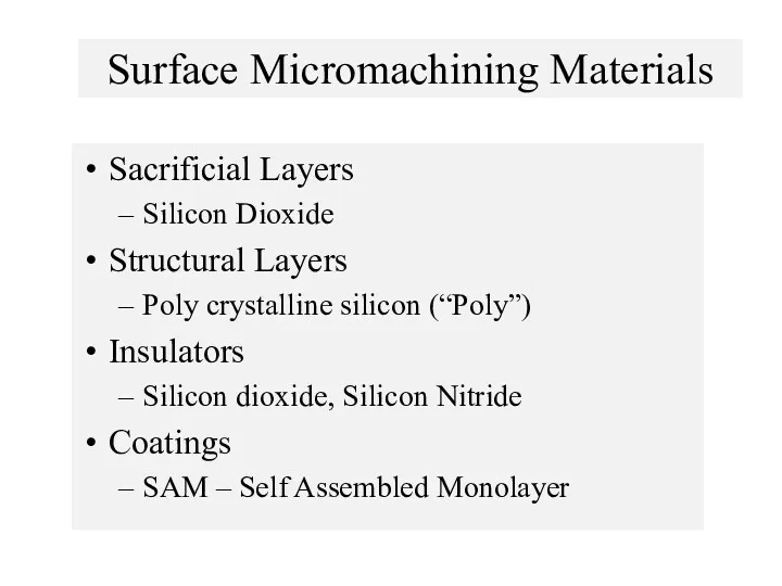
Surface Micromachining Materials
Sacrificial Layers
Silicon Dioxide
Structural Layers
Poly crystalline silicon (“Poly”)
Insulators
Silicon dioxide, Silicon
Surface Micromachining Materials
Sacrificial Layers
Silicon Dioxide
Structural Layers
Poly crystalline silicon (“Poly”)
Insulators
Silicon dioxide, Silicon
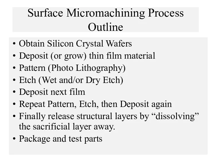
Surface Micromachining Process Outline
Obtain Silicon Crystal Wafers
Deposit (or grow) thin film
Surface Micromachining Process Outline
Obtain Silicon Crystal Wafers
Deposit (or grow) thin film
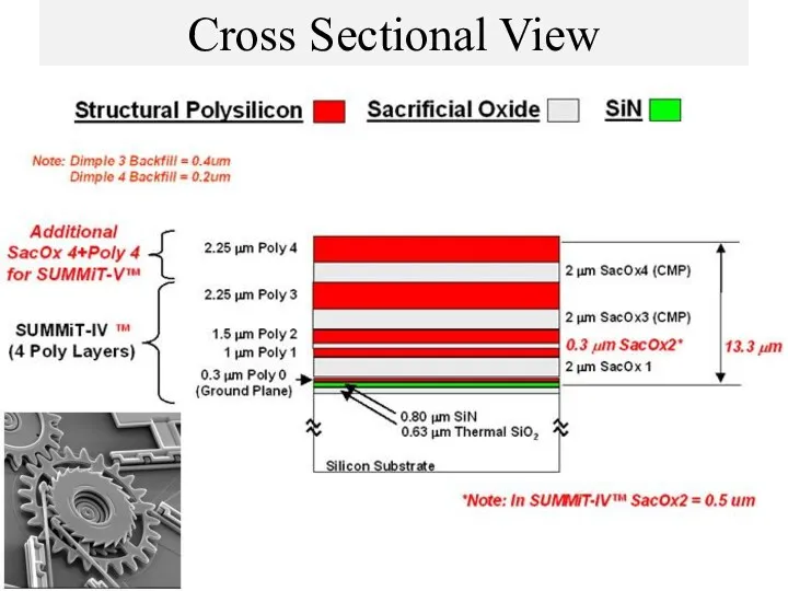
Cross Sectional View
Cross Sectional View
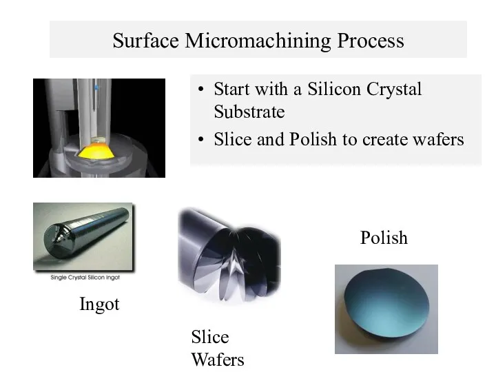
Surface Micromachining Process
Start with a Silicon Crystal Substrate
Slice and Polish to
Surface Micromachining Process
Start with a Silicon Crystal Substrate
Slice and Polish to
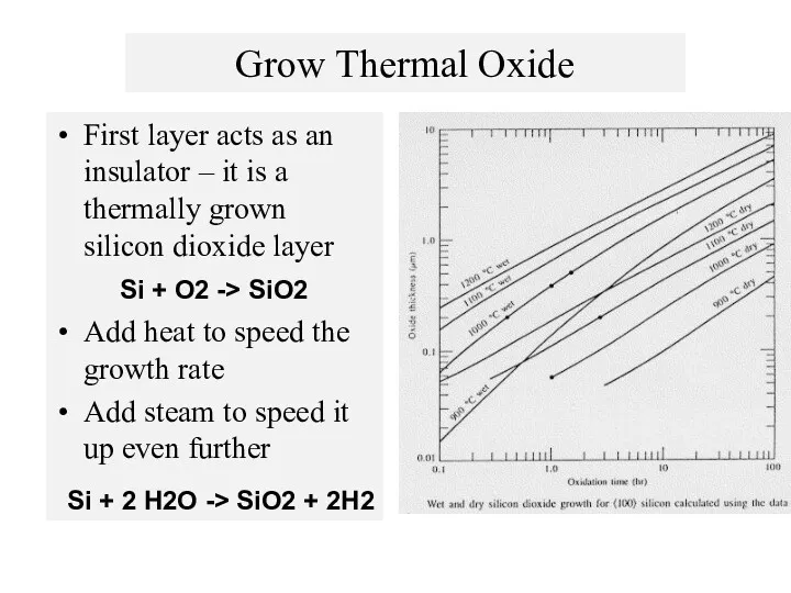
Grow Thermal Oxide
First layer acts as an insulator – it is
Grow Thermal Oxide
First layer acts as an insulator – it is
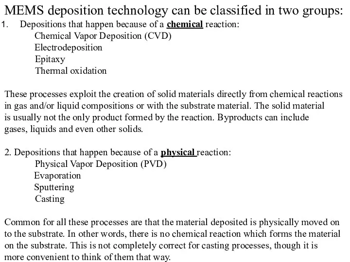
MEMS deposition technology can be classified in two groups:
Depositions that
MEMS deposition technology can be classified in two groups:
Depositions that
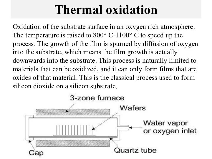
Thermal oxidation
Oxidation of the substrate surface in an oxygen rich atmosphere.
Thermal oxidation
Oxidation of the substrate surface in an oxygen rich atmosphere.
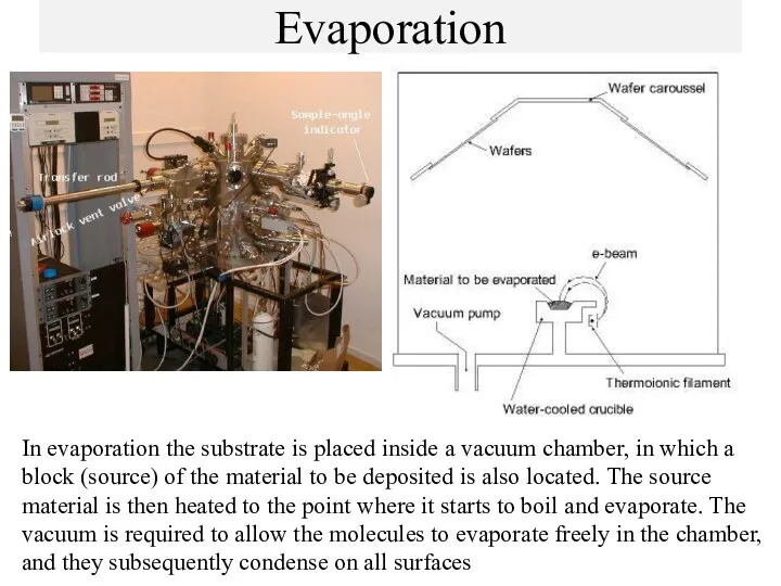
Evaporation
In evaporation the substrate is placed inside a vacuum chamber, in
Evaporation
In evaporation the substrate is placed inside a vacuum chamber, in
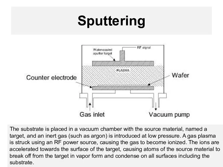
Sputtering
The substrate is placed in a vacuum chamber with the source
Sputtering
The substrate is placed in a vacuum chamber with the source
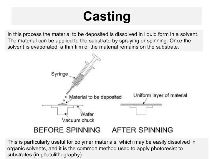
Casting
In this process the material to be deposited is dissolved in
Casting
In this process the material to be deposited is dissolved in
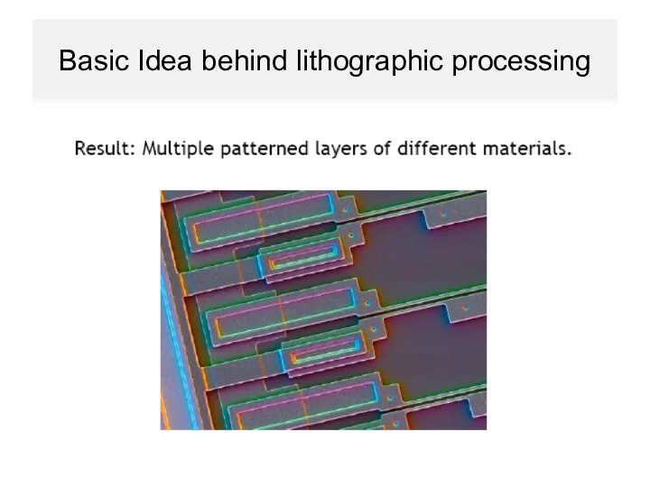
Basic Idea behind lithographic processing
Basic Idea behind lithographic processing
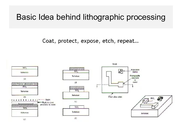
Basic Idea behind lithographic processing
Basic Idea behind lithographic processing
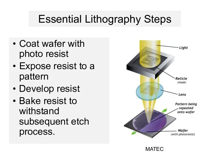
Essential Lithography Steps
Coat wafer with photo resist
Expose resist to a pattern
Develop
Essential Lithography Steps
Coat wafer with photo resist
Expose resist to a pattern
Develop
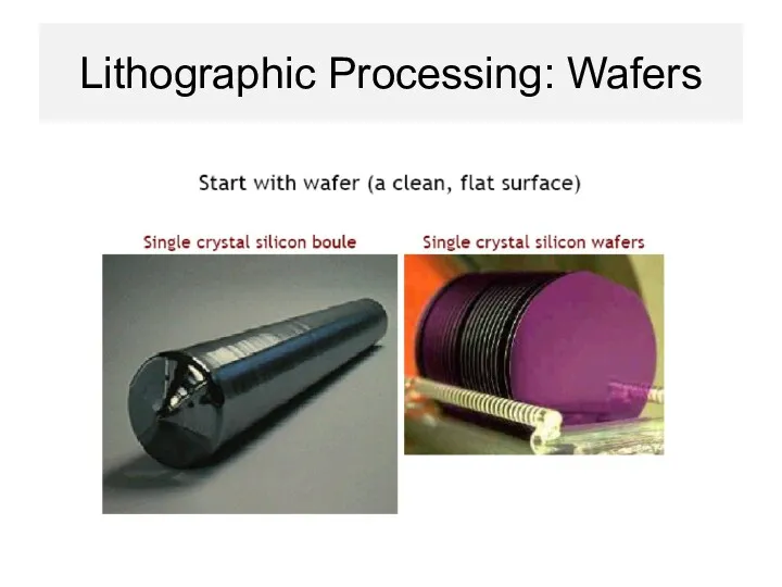
Lithographic Processing: Wafers
Lithographic Processing: Wafers
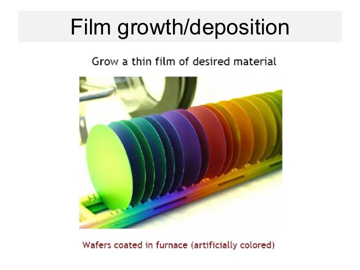
Film growth/deposition
Film growth/deposition
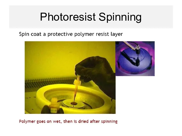
Photoresist Spinning
Photoresist Spinning
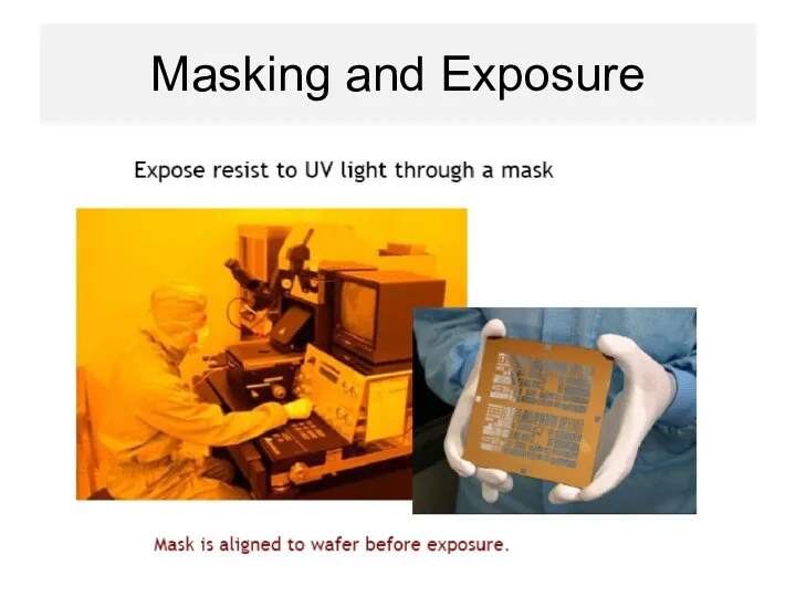
Masking and Exposure
Masking and Exposure
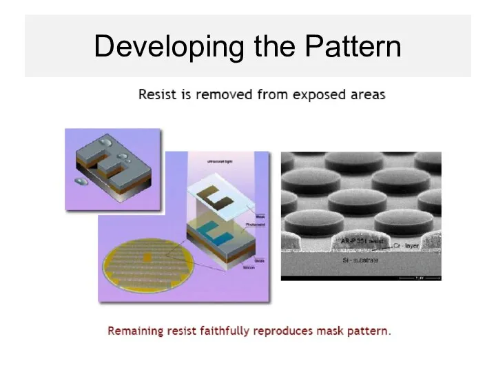
Developing the Pattern
Developing the Pattern
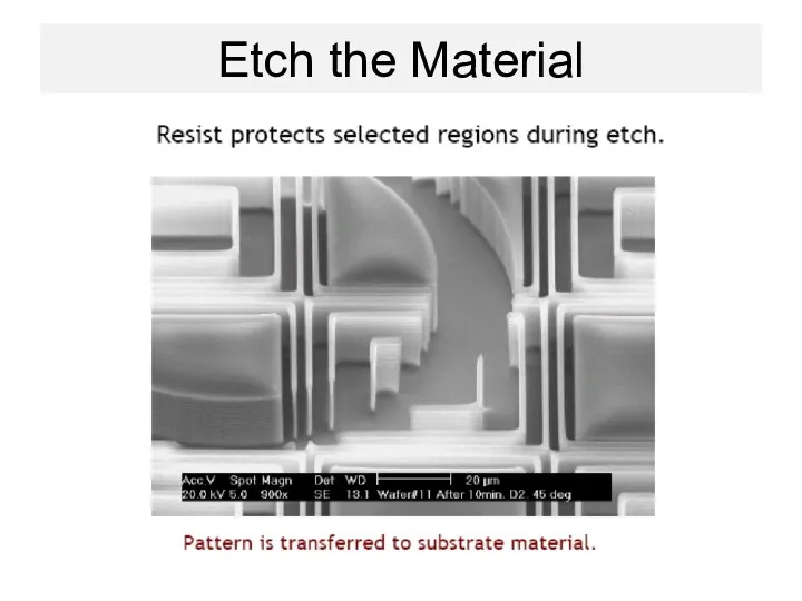
Etch the Material
Etch the Material
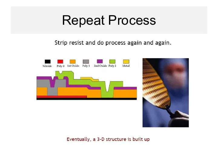
Repeat Process
Repeat Process
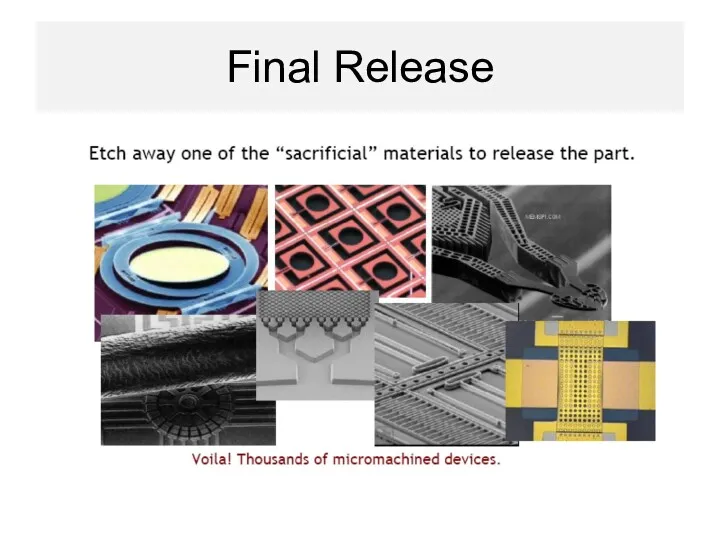
Final Release
Final Release
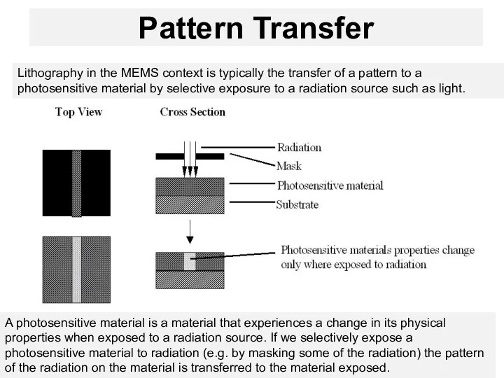
Pattern Transfer
Lithography in the MEMS context is typically the transfer of
Pattern Transfer
Lithography in the MEMS context is typically the transfer of
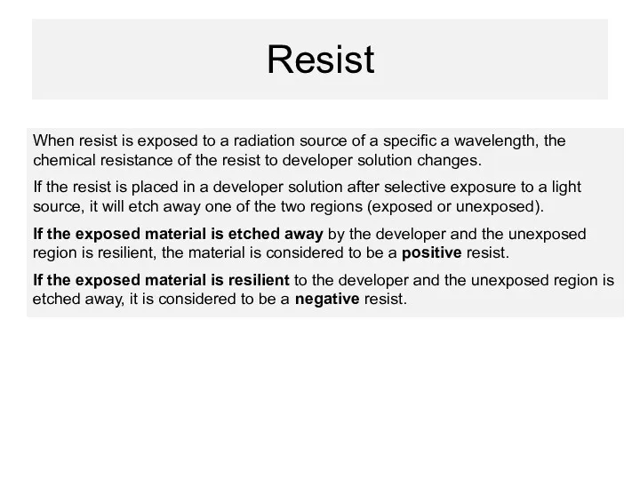
Resist
When resist is exposed to a radiation source of a specific
Resist
When resist is exposed to a radiation source of a specific
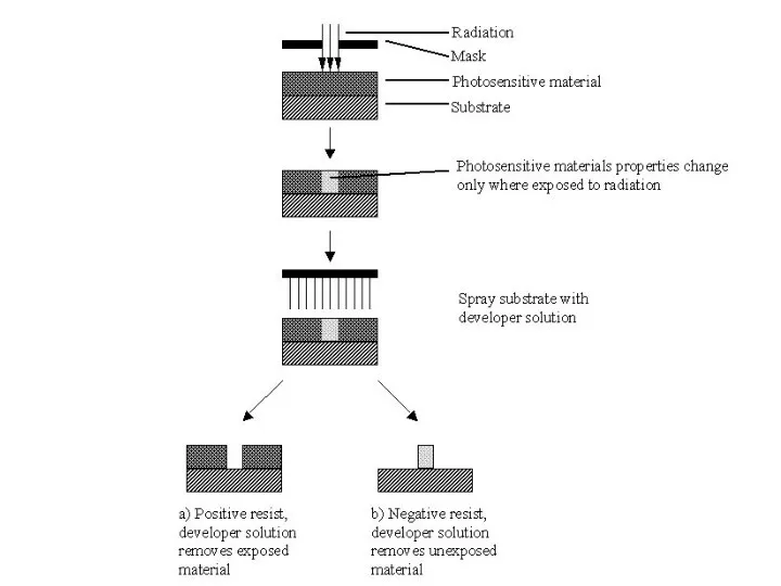
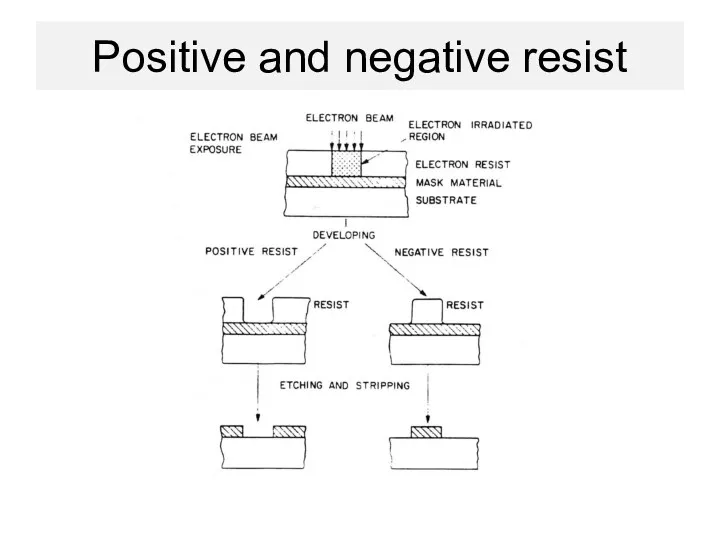
Positive and negative resist
Positive and negative resist
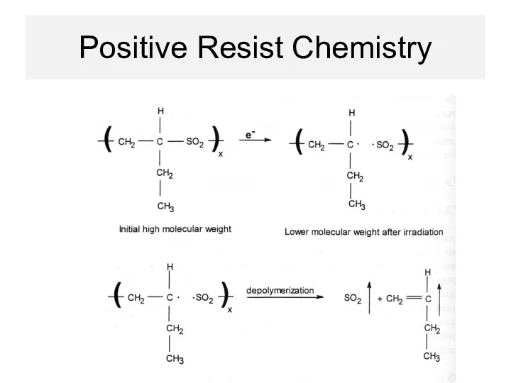
Positive Resist Chemistry
Positive Resist Chemistry
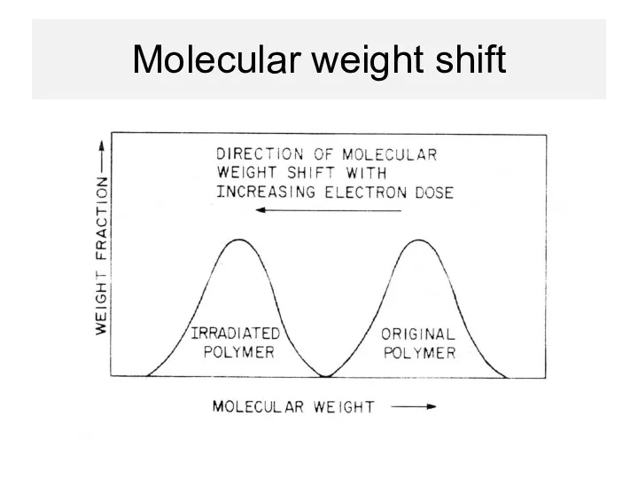
Molecular weight shift
Molecular weight shift
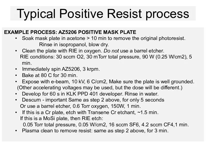
Typical Positive Resist process
EXAMPLE PROCESS: AZ5206 POSITIVE MASK PLATE
Soak mask plate
Typical Positive Resist process
EXAMPLE PROCESS: AZ5206 POSITIVE MASK PLATE
Soak mask plate
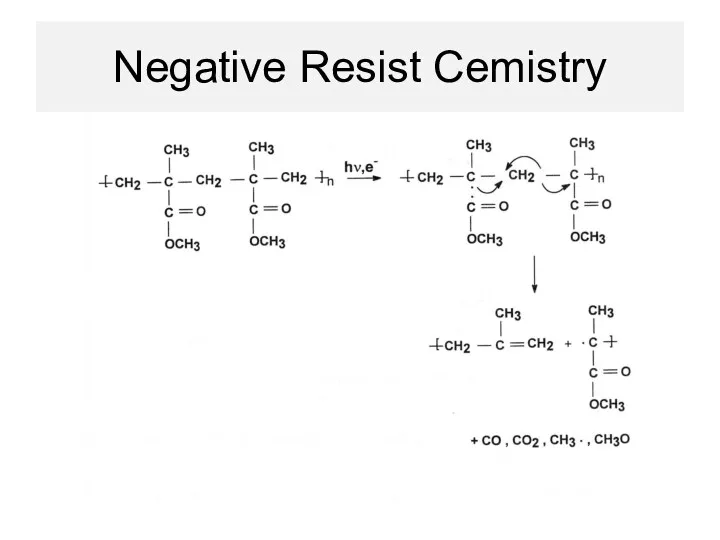
Negative Resist Cemistry
Negative Resist Cemistry
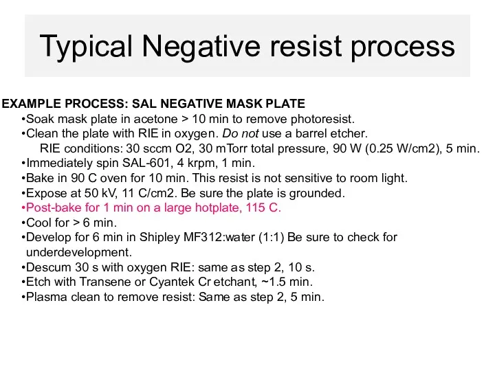
Typical Negative resist process
EXAMPLE PROCESS: SAL NEGATIVE MASK PLATE
Soak mask plate
Typical Negative resist process
EXAMPLE PROCESS: SAL NEGATIVE MASK PLATE
Soak mask plate
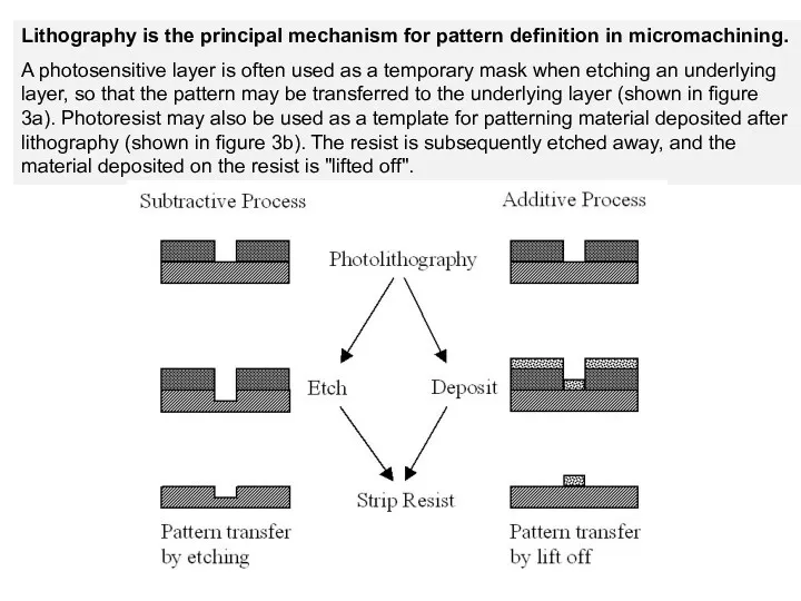
Lithography is the principal mechanism for pattern definition in micromachining.
A
Lithography is the principal mechanism for pattern definition in micromachining.
A
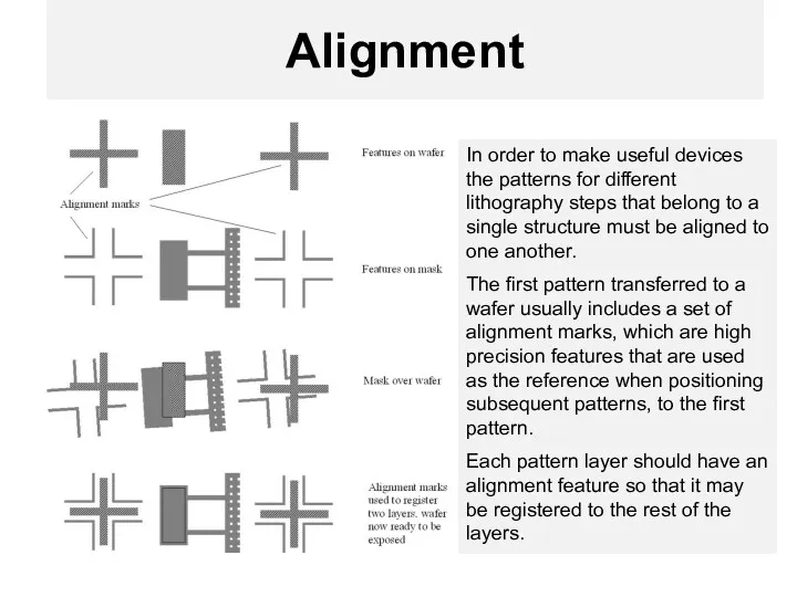
Alignment
In order to make useful devices the patterns for different lithography
Alignment
In order to make useful devices the patterns for different lithography
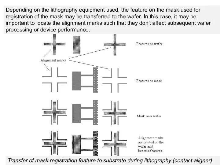
Depending on the lithography equipment used, the feature on the mask
Depending on the lithography equipment used, the feature on the mask
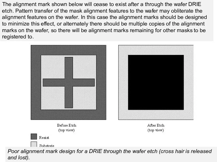
Poor alignment mark design for a DRIE through the wafer etch
Poor alignment mark design for a DRIE through the wafer etch
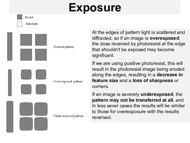
Exposure
At the edges of pattern light is scattered and diffracted, so
Exposure
At the edges of pattern light is scattered and diffracted, so
The Lithography Module
Dehydration bake - dehydrate the wafer to aid resist
The Lithography Module
Dehydration bake - dehydrate the wafer to aid resist
Etching
In order to form a functional MEMS structure on a substrate,
Etching
In order to form a functional MEMS structure on a substrate,
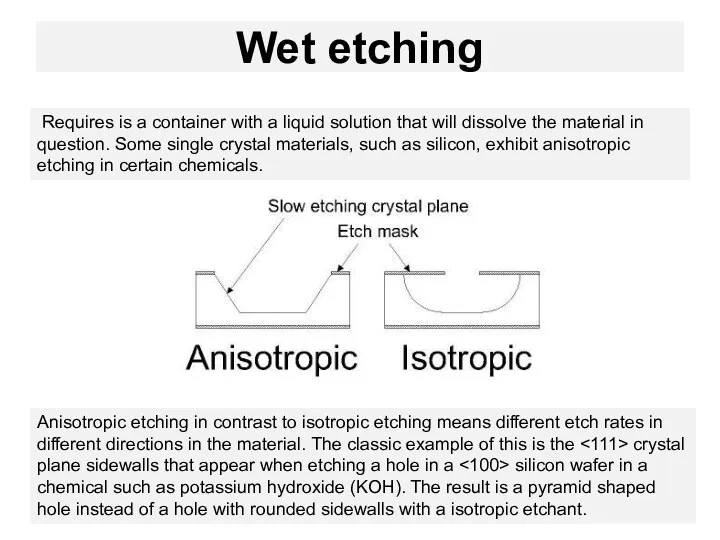
Wet etching
Requires is a container with a liquid solution that
Wet etching
Requires is a container with a liquid solution that
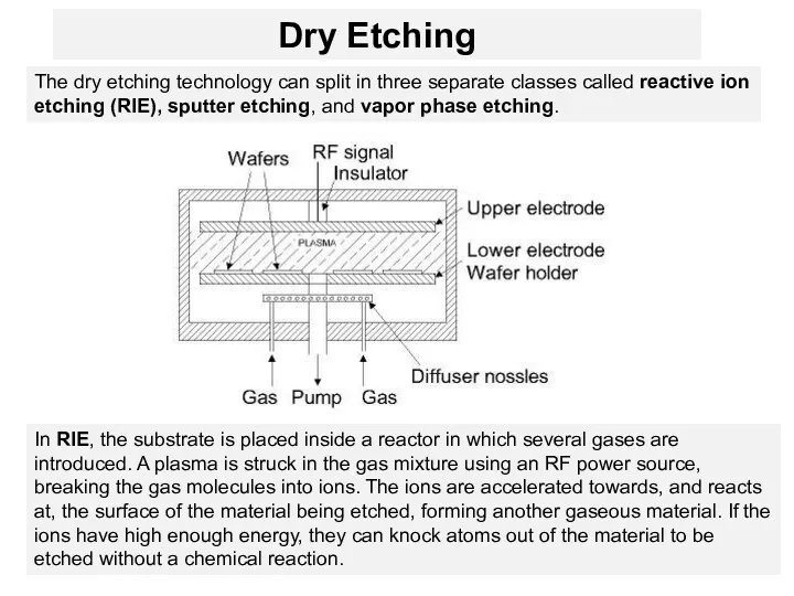
Dry Etching
In RIE, the substrate is placed inside a reactor in
Dry Etching
In RIE, the substrate is placed inside a reactor in
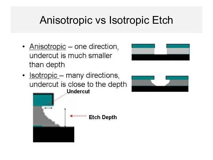
Anisotropic vs Isotropic Etch
Anisotropic vs Isotropic Etch
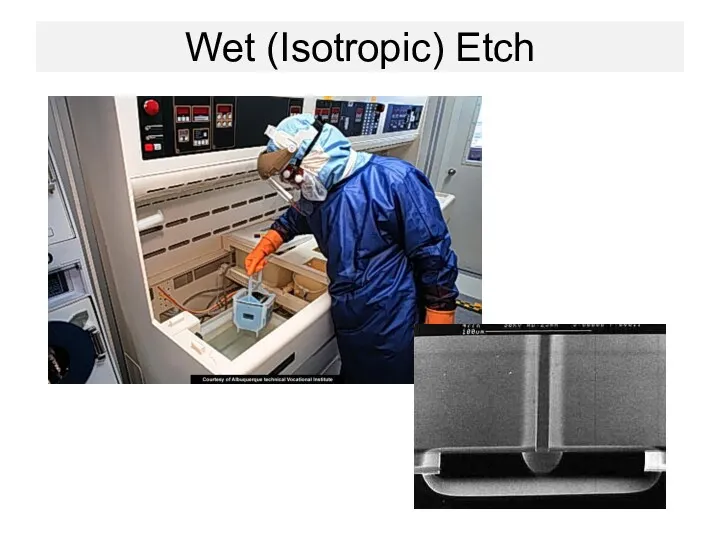
Wet (Isotropic) Etch
Wet (Isotropic) Etch
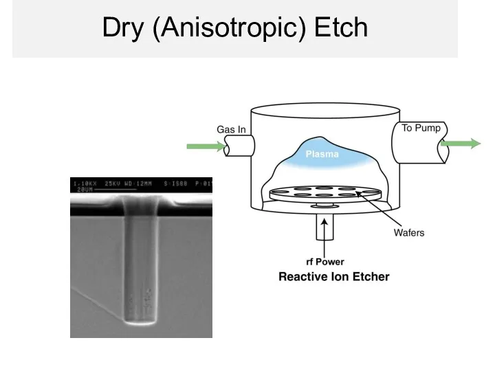
Dry (Anisotropic) Etch
Dry (Anisotropic) Etch
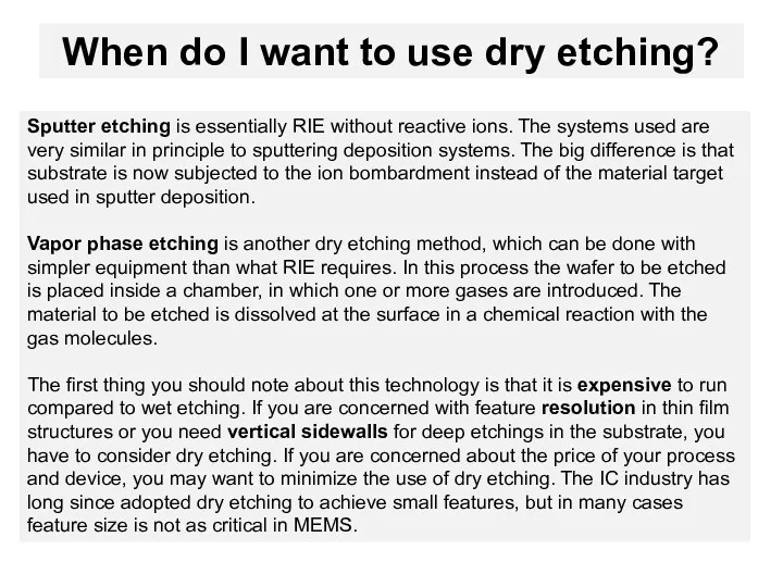
Sputter etching is essentially RIE without reactive ions. The systems used
Sputter etching is essentially RIE without reactive ions. The systems used
Wafer Example
Design Masks
Silicon Substrate
Deposit 5K Oxide
Pattern Mask 1
Wet Etch (Timed
Wafer Example
Design Masks
Silicon Substrate
Deposit 5K Oxide
Pattern Mask 1
Wet Etch (Timed
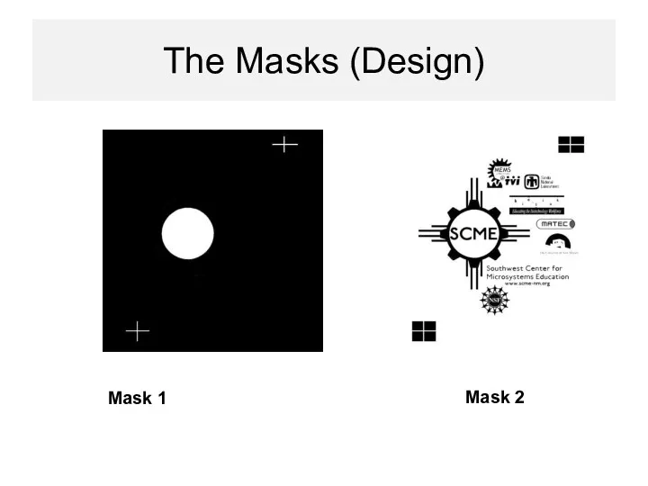
The Masks (Design)
Mask 1
Mask 2
The Masks (Design)
Mask 1
Mask 2
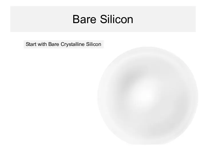
Bare Silicon
Start with Bare Crystalline Silicon
Bare Silicon
Start with Bare Crystalline Silicon
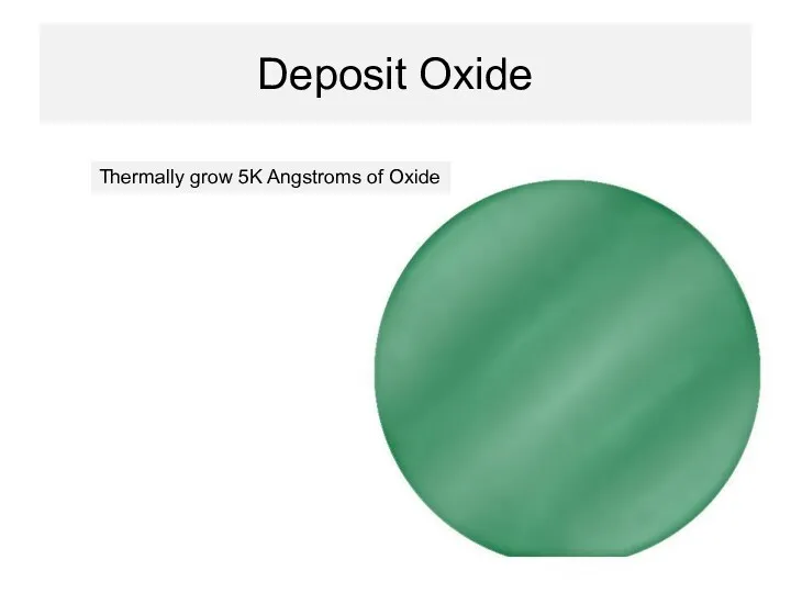
Deposit Oxide
Thermally grow 5K Angstroms of Oxide
Deposit Oxide
Thermally grow 5K Angstroms of Oxide
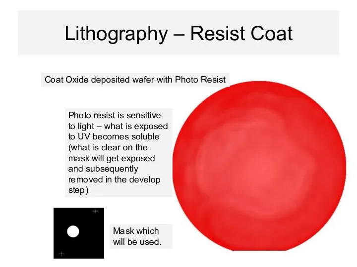
Lithography – Resist Coat
Coat Oxide deposited wafer with Photo Resist
Photo resist
Lithography – Resist Coat
Coat Oxide deposited wafer with Photo Resist
Photo resist
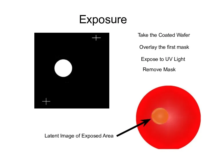
Exposure
Take the Coated Wafer
Overlay the first mask
Expose to UV Light
Remove Mask
Exposure
Take the Coated Wafer
Overlay the first mask
Expose to UV Light
Remove Mask
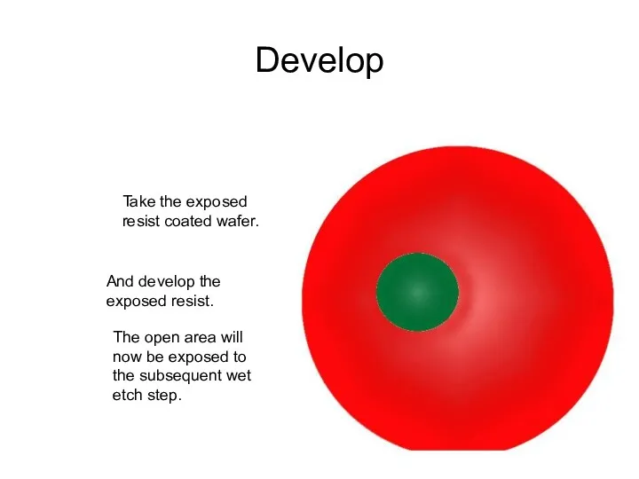
Develop
Take the exposed resist coated wafer.
And develop the exposed resist.
The open
Develop
Take the exposed resist coated wafer.
And develop the exposed resist.
The open
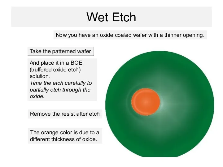
Wet Etch
The orange color is due to a different thickness of
Wet Etch
The orange color is due to a different thickness of
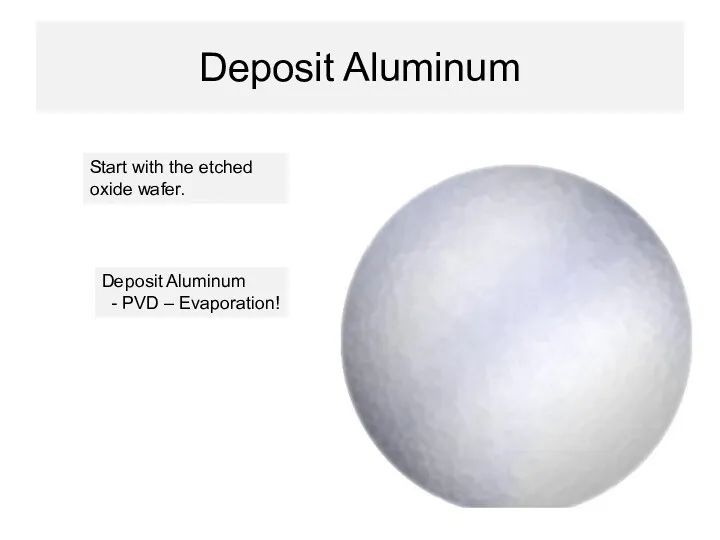
Deposit Aluminum
Start with the etched oxide wafer.
Deposit Aluminum
Start with the etched oxide wafer.
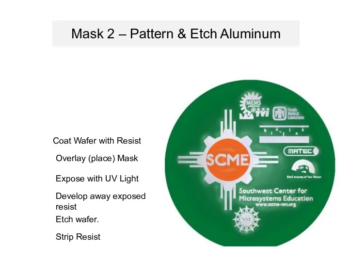
Mask 2 – Pattern & Etch Aluminum
Expose with UV Light
Mask 2 – Pattern & Etch Aluminum
Expose with UV Light
Electron Beam Lithography
Electron Beam Lithography
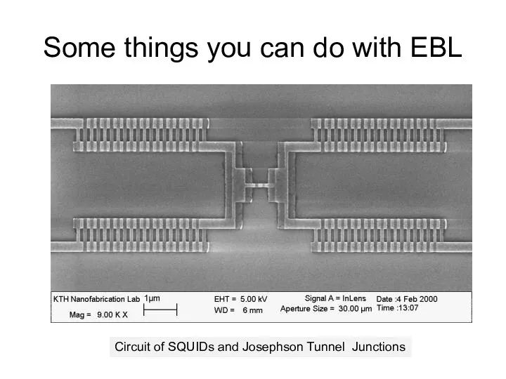
Some things you can do with EBL
Circuit of SQUIDs and Josephson
Some things you can do with EBL
Circuit of SQUIDs and Josephson
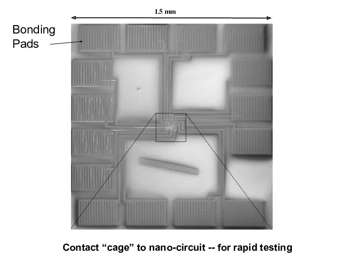
1.5 mm
Contact “cage” to nano-circuit -- for rapid testing
Bonding Pads
1.5 mm
Contact “cage” to nano-circuit -- for rapid testing
Bonding Pads
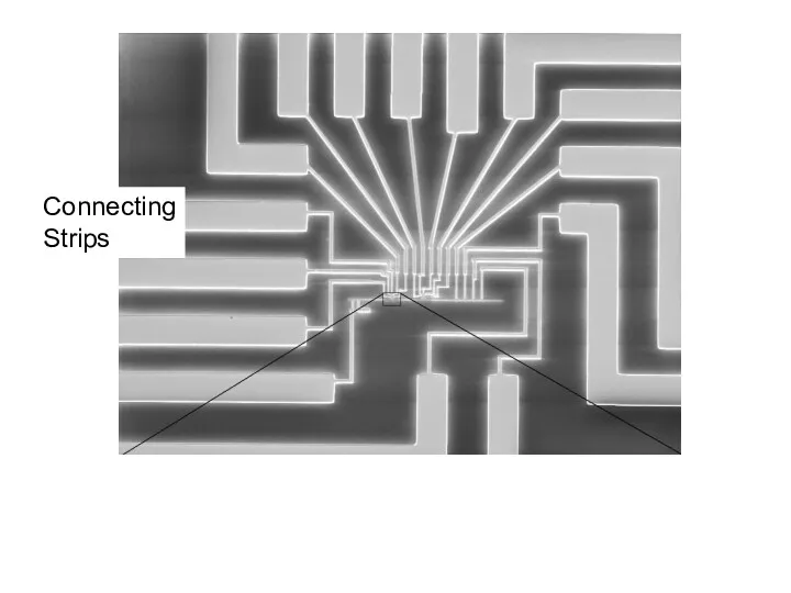
Connecting
Strips
Connecting
Strips
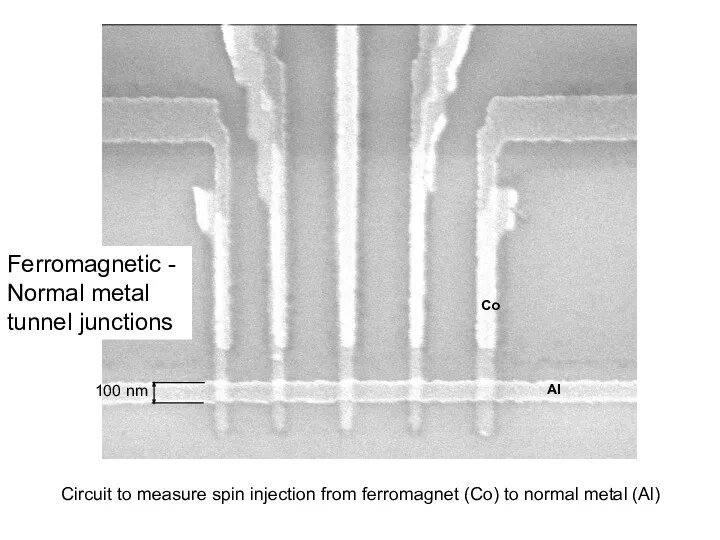
100 nm
Al
Co
Circuit to measure spin injection from ferromagnet (Co) to normal
100 nm
Al
Co
Circuit to measure spin injection from ferromagnet (Co) to normal
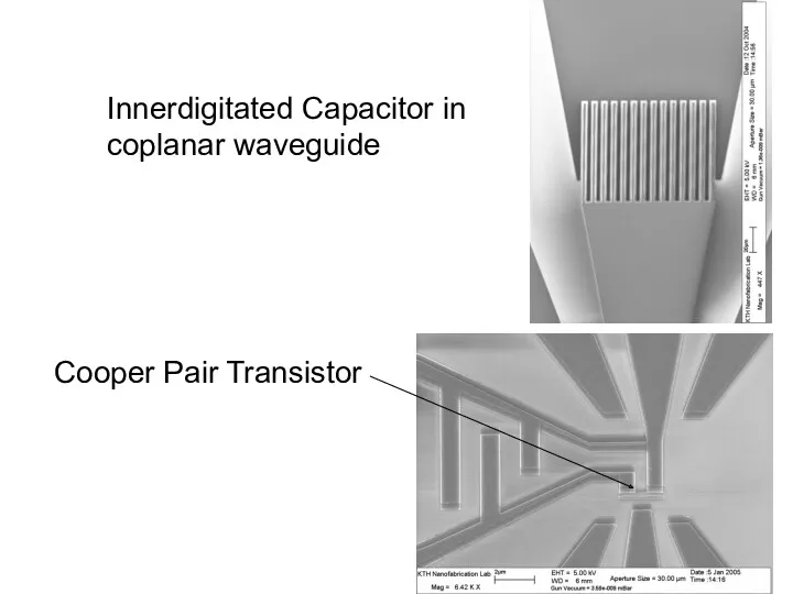
Innerdigitated Capacitor in
coplanar waveguide
Cooper Pair Transistor
Innerdigitated Capacitor in
coplanar waveguide
Cooper Pair Transistor
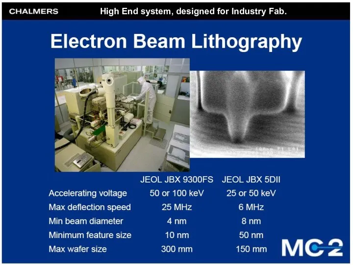
High End system, designed for Industry Fab.
High End system, designed for Industry Fab.
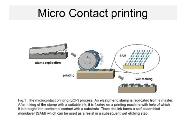
Micro Contact printing
Micro Contact printing
 Impressionism. Claude Monet
 Лекція 18 new
 Денсаулықты кешенді бағалау денсаулық критерилері және денсаулық топтарын құрастыру
 Жилищный фонд, его виды. Переустройство и перепланировка жилых помещений. Жилищный надзор и жилищный контроль
 75 лет Великой Победы!
 Промышленная безопасность
 Радіоелектронний захист ЗРЛ. Методи захисту від активних перешкод (Заняття №5.2)
 Тепловые методы увеличения нефтеотдачи
 Процесс очистки внутренней полости нефте- и нефтепродуктопроводов
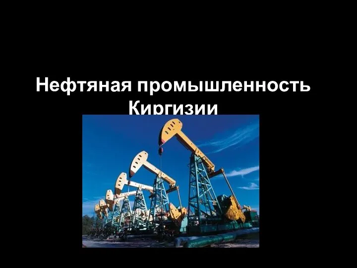 Нефтяная промышленность Киргизии
 материал к уроку Электромагнитные колебания.История открытия. 11 класс .профильный курс.Лекция с использованием презентации.
 Монашество. Иоанн Шанхайский
 City Tour Tbilisi 35 lari
 Дети моей группы Звёздочки
 Введение. Элементная база электронных устройств. Лекция 1
 Отопление зданий
 Женские лица российской прозы
 Незабываемое поздравление для мужчин
 Классный час по теме: Государственные символы России
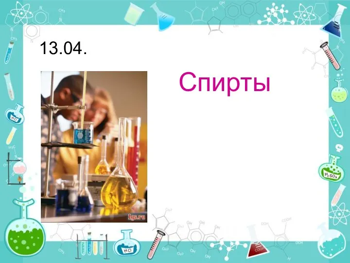 Урок по теме Спирты
 Тренажер по русскому языку Родовые окончания имён прилагательных
 Нейрогуморальная регуляция полового процесса
 Мини-музей в ДОУ
 Детские праздники и дни рождения Лазертаг
 История развития тифлопедагогики
 Архитектурные памятники Липецкой области
 Родительское собрание Первые школьные отметки
 Спортсмены-паралимпийцы Оренбургской области