- Microelectromechanical Systems (MEMS) An introduction

Содержание
- 2. Outline Introduction Applications Passive structures Sensors Actuators Future Applications MEMS micromachining technology Bulk micromachining Surface micromachining
- 3. What are MEMS? (Micro-electromechanical Systems) Fabricated using micromachining technology Used for sensing, actuation or are passive
- 4. 3-D Micromachined Structures Linear Rack Gear Reduction Drive Triple-Piston Microsteam Engine Photos from Sandia National Lab.
- 5. 3-D Micromachined Structures Movies from Sandia National Lab. Website: http://mems.sandia.gov 2 dust mites on an optical
- 6. Applications: Passive Structures Inkjet Printer Nozzle
- 7. Applications: Sensors Pressure sensor: Piezoresistive sensing Capacitive sensing Resonant sensing Application examples: Manifold absolute pressure (MAP)
- 8. Piezoresistive Pressure Sensors
- 9. Piezoresistive Pressure Sensors Wheatstone Bridge configuration Illustration from “An Introduction to MEMS Engineering”, N. Maluf
- 10. Applications: Sensors Acceleration Air bag crash sensing Seat belt tension Automobile suspension control Human activity for
- 11. Accelerometers
- 12. Accelerometers Accelerometer parameters acceleration range (G) (1G=9.81 m/s2) sensitivity (V/G) resolution (G) bandwidth (Hz) cross axis
- 13. Capacitive Accelerometers Stationary Polysilicon fingers Based on ADXL accelerometers, Analog Devices, Inc. Spring Inertial Mass Anchor
- 14. Applications: Actuators Texas Instruments Digital Micromirror DeviceTM Array of up to 1.3 million mirrors Invented by
- 15. Digital Micromirror Device From “An Introduction to Microelectromechanical Systems Engineering” by Nadim Maluf
- 16. Digital Micromirror Device From “An Introduction to Microelectromechanical Systems Engineering” by Nadim Maluf => Acheive grey
- 17. Some future applications Biological applications: Microfluidics Lab-on-a-Chip Micropumps Resonant microbalances Micro Total Analysis systems Mobile communications:
- 18. Microfluidics / DNA Analysis
- 19. Basic microfabrication technologies Deposition Chemical vapor deposition (CVD/PECVD/LPCVD) Epitaxy Oxidation Evaporation Sputtering Spin-on methods Etching Wet
- 20. Bulk micromachining Anisotropic etching of silicon
- 21. Bulk micromachining Anisotropic etch of {100} Si 54.74º a 0.707a
- 22. Bulk micromachining: Pressure sensors Piezoresistive elements SiO2 p+ Si Si
- 23. Surface Micromachining substrate Important issues: selectivity of structural, sacrificial and substrate materials stress of structural material
- 24. Surface Micromachining Most commonly used materials for surface micromachining: substrate: silicon sacrificial material: SiO2 or phosphosilicate
- 25. Surface Micromachining Polysilicon deposited by LPCVD (T~600 ºC) usually has large stress High T anneal (600-1000
- 26. Surface Micromachining Surface tension of liquid during evaporation results in capillary forces that causes the structures
- 27. LIGA – X-ray Lithography, Electroplating (Galvanoformung), Molding (Abformung) Deposit plating base Deposit photoresist Expose and develop
- 28. LIGA Photos from MCNC – MEMS group
- 29. Wafer bonding- Anodic bring sodium contating glass (Pyrex) and silicon together heat to high temperature (200-500
- 30. Summary: MEMS fabrication MEMS technology is based on silicon microelectronics technology Main MEMS techniques Bulk micromachining
- 31. Thin-film MEMS Thin films allows: Low-temperature processing Large area, low cost, flexible or biocompatible substrates Possibility
- 32. d=1 μm; h=500 nm; b=10 μm Lmax(bridge) ~ 60 μm ; Lmax(cantilever) ~ 30 μm Surface
- 33. Electrostatic force between gate and counter-electrode Electrostatic force is always attractive Electrostatic Actuation
- 34. A laser beam is focused on the structure and the reflected light is collected with an
- 35. Optical detection of electrical actuation Resonance is inversely proportional to square of the length 20 MHz
- 37. Скачать презентацию
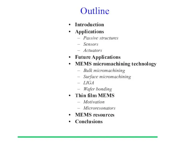
Outline
Introduction
Applications
Passive structures
Sensors
Actuators
Future Applications
MEMS micromachining technology
Bulk micromachining
Surface micromachining
LIGA
Wafer bonding
Thin film MEMS
Motivation
Microresonators
MEMS resources
Conclusions
Outline
Introduction
Applications
Passive structures
Sensors
Actuators
Future Applications
MEMS micromachining technology
Bulk micromachining
Surface micromachining
LIGA
Wafer bonding
Thin film MEMS
Motivation
Microresonators
MEMS resources
Conclusions
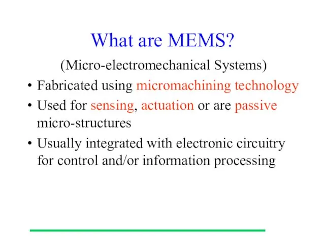
What are MEMS?
(Micro-electromechanical Systems)
Fabricated using micromachining technology
Used for sensing, actuation or
What are MEMS?
(Micro-electromechanical Systems)
Fabricated using micromachining technology
Used for sensing, actuation or
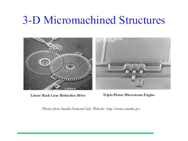
3-D Micromachined Structures
Linear Rack Gear Reduction Drive
Triple-Piston Microsteam Engine
Photos
3-D Micromachined Structures
Linear Rack Gear Reduction Drive
Triple-Piston Microsteam Engine
Photos
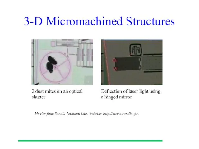
3-D Micromachined Structures
Movies from Sandia National Lab. Website: http://mems.sandia.gov
2 dust mites
3-D Micromachined Structures
Movies from Sandia National Lab. Website: http://mems.sandia.gov
2 dust mites
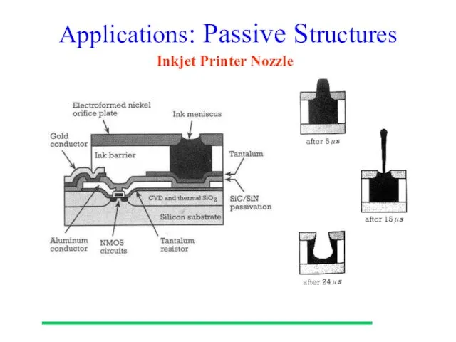
Applications: Passive Structures
Inkjet Printer Nozzle
Applications: Passive Structures
Inkjet Printer Nozzle
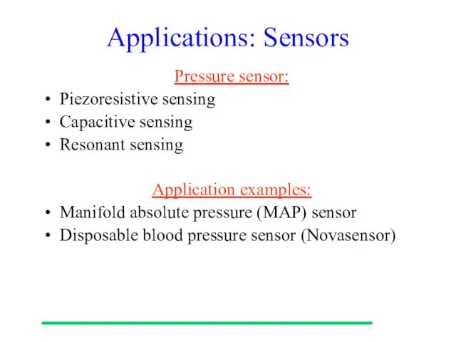
Applications: Sensors
Pressure sensor:
Piezoresistive sensing
Capacitive sensing
Resonant sensing
Application examples:
Manifold absolute pressure (MAP) sensor
Disposable
Applications: Sensors
Pressure sensor:
Piezoresistive sensing
Capacitive sensing
Resonant sensing
Application examples:
Manifold absolute pressure (MAP) sensor
Disposable
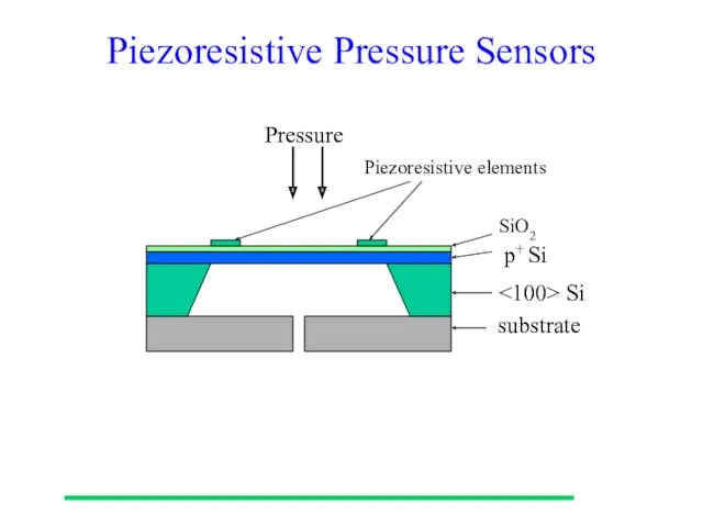
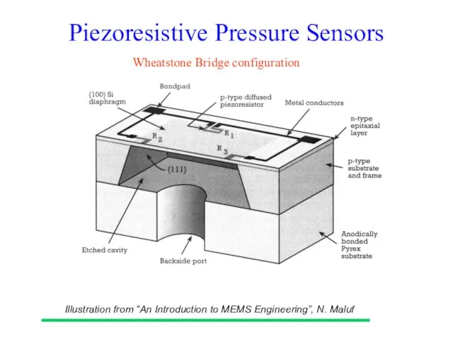
Piezoresistive Pressure Sensors
Piezoresistive Pressure Sensors
Piezoresistive Pressure Sensors
Wheatstone Bridge configuration
Illustration from “An Introduction to MEMS Engineering”,
Piezoresistive Pressure Sensors
Wheatstone Bridge configuration
Illustration from “An Introduction to MEMS Engineering”,
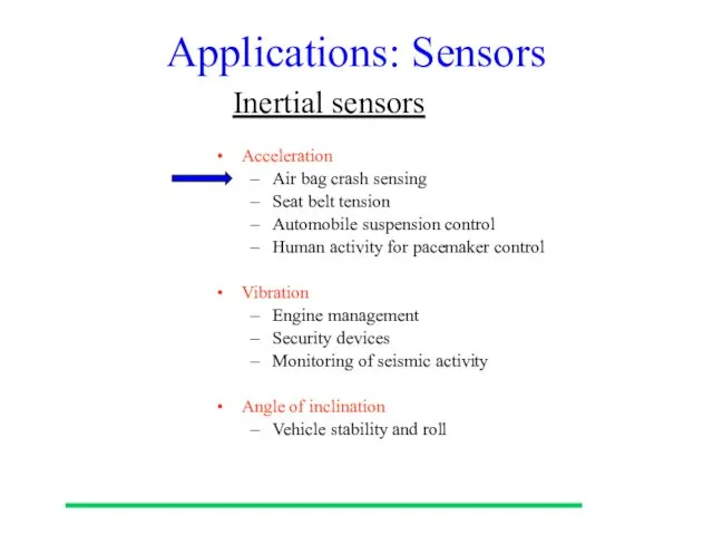
Applications: Sensors
Acceleration
Air bag crash sensing
Seat belt tension
Automobile suspension control
Human activity for
Applications: Sensors
Acceleration
Air bag crash sensing
Seat belt tension
Automobile suspension control
Human activity for
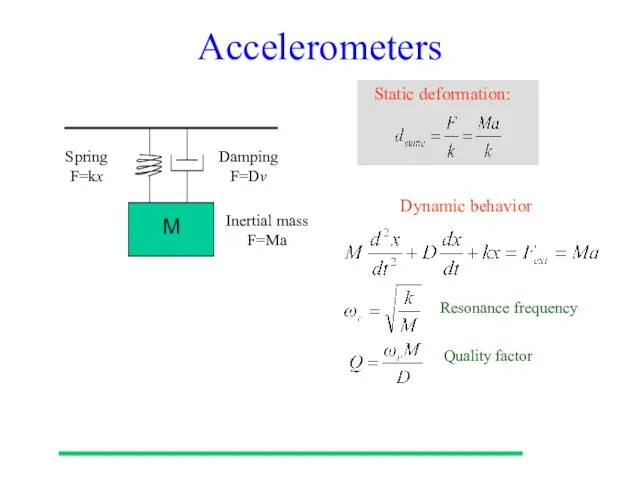
Accelerometers
Accelerometers
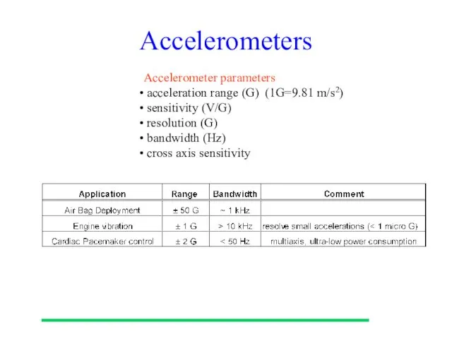
Accelerometers
Accelerometer parameters
acceleration range (G) (1G=9.81 m/s2)
sensitivity (V/G)
resolution (G)
Accelerometers
Accelerometer parameters
acceleration range (G) (1G=9.81 m/s2)
sensitivity (V/G)
resolution (G)
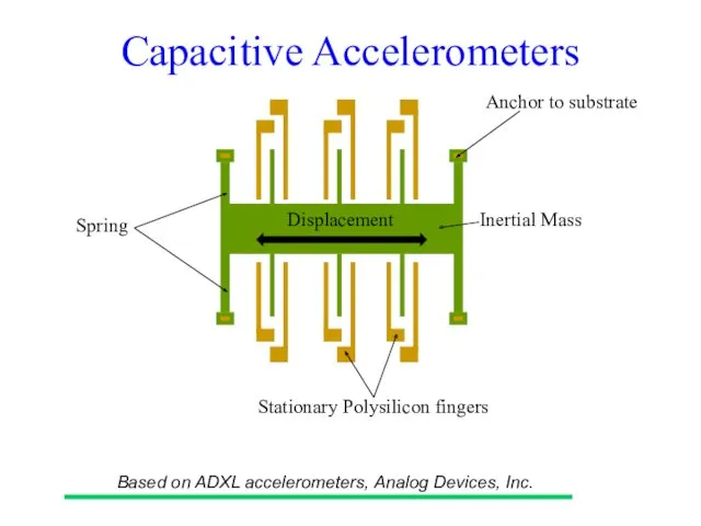
Capacitive Accelerometers
Stationary Polysilicon fingers
Based on ADXL accelerometers, Analog Devices, Inc.
Spring
Inertial Mass
Anchor
Capacitive Accelerometers
Stationary Polysilicon fingers
Based on ADXL accelerometers, Analog Devices, Inc.
Spring
Inertial Mass
Anchor
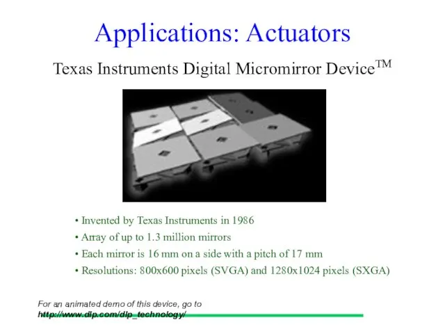
Applications: Actuators
Texas Instruments Digital Micromirror DeviceTM
Array of up to 1.3
Applications: Actuators
Texas Instruments Digital Micromirror DeviceTM
Array of up to 1.3
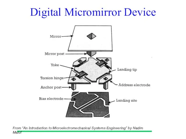
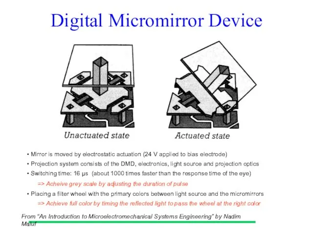
Digital Micromirror Device
From “An Introduction to Microelectromechanical Systems Engineering” by Nadim
Digital Micromirror Device
From “An Introduction to Microelectromechanical Systems Engineering” by Nadim
Digital Micromirror Device
From “An Introduction to Microelectromechanical Systems Engineering” by Nadim
Digital Micromirror Device
From “An Introduction to Microelectromechanical Systems Engineering” by Nadim
Some future applications
Biological applications:
Microfluidics
Lab-on-a-Chip
Micropumps
Resonant microbalances
Micro Total Analysis systems
Mobile communications:
Micromechanical resonator
Some future applications
Biological applications:
Microfluidics
Lab-on-a-Chip
Micropumps
Resonant microbalances
Micro Total Analysis systems
Mobile communications:
Micromechanical resonator
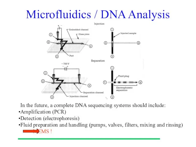
Microfluidics / DNA Analysis
Microfluidics / DNA Analysis
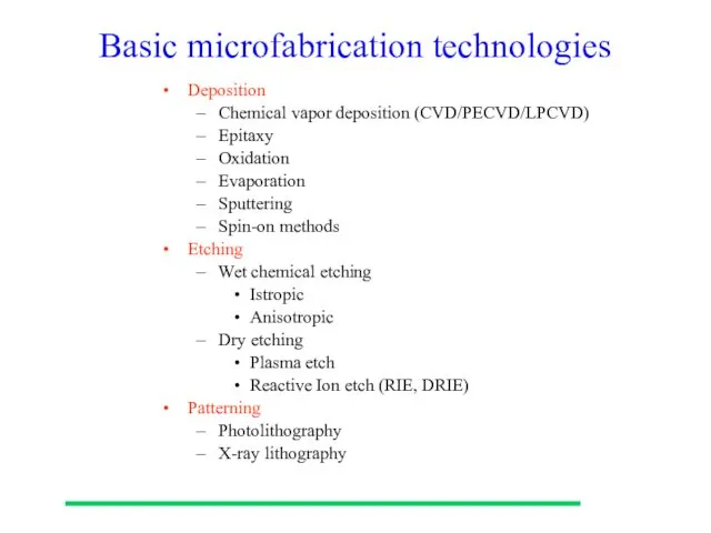
Basic microfabrication technologies
Deposition
Chemical vapor deposition (CVD/PECVD/LPCVD)
Epitaxy
Oxidation
Evaporation
Sputtering
Spin-on methods
Etching
Wet chemical etching
Istropic
Anisotropic
Dry etching
Plasma etch
Reactive
Basic microfabrication technologies
Deposition
Chemical vapor deposition (CVD/PECVD/LPCVD)
Epitaxy
Oxidation
Evaporation
Sputtering
Spin-on methods
Etching
Wet chemical etching
Istropic
Anisotropic
Dry etching
Plasma etch
Reactive
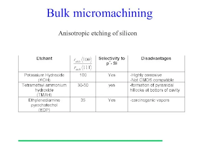
Bulk micromachining
Anisotropic etching of silicon
Bulk micromachining
Anisotropic etching of silicon
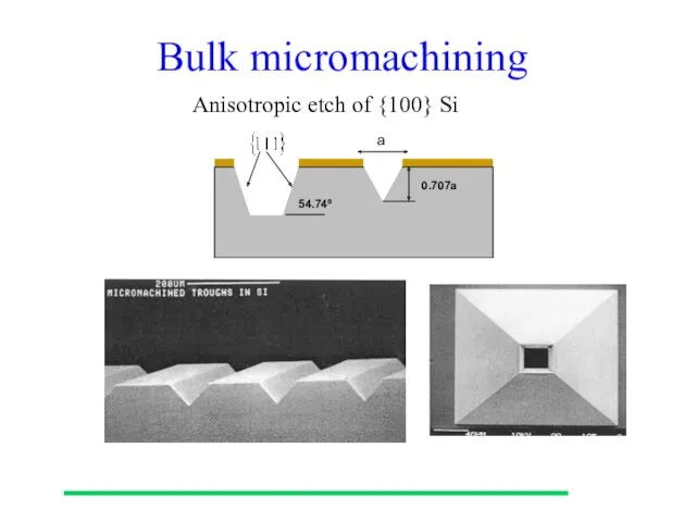
Bulk micromachining
Anisotropic etch of {100} Si
54.74º
a
0.707a
Bulk micromachining
Anisotropic etch of {100} Si
54.74º
a
0.707a
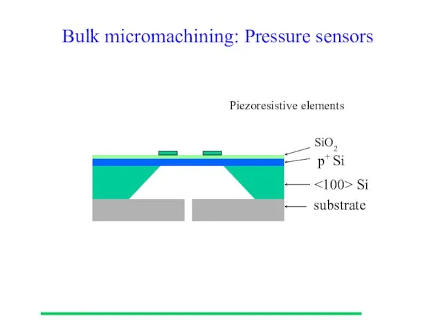
Bulk micromachining: Pressure sensors
Piezoresistive elements
SiO2
p+ Si
<100> Si
Bulk micromachining: Pressure sensors
Piezoresistive elements
SiO2
p+ Si
<100> Si
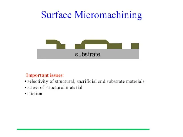
Surface Micromachining
substrate
Important issues:
selectivity of structural, sacrificial and substrate materials
stress
Surface Micromachining
substrate
Important issues:
selectivity of structural, sacrificial and substrate materials
stress
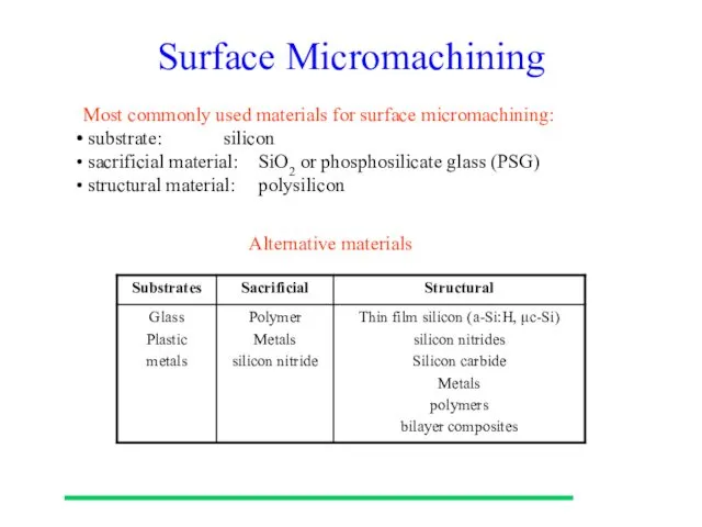
Surface Micromachining
Most commonly used materials for surface micromachining:
substrate: silicon
sacrificial material: SiO2
Surface Micromachining
Most commonly used materials for surface micromachining:
substrate: silicon
sacrificial material: SiO2
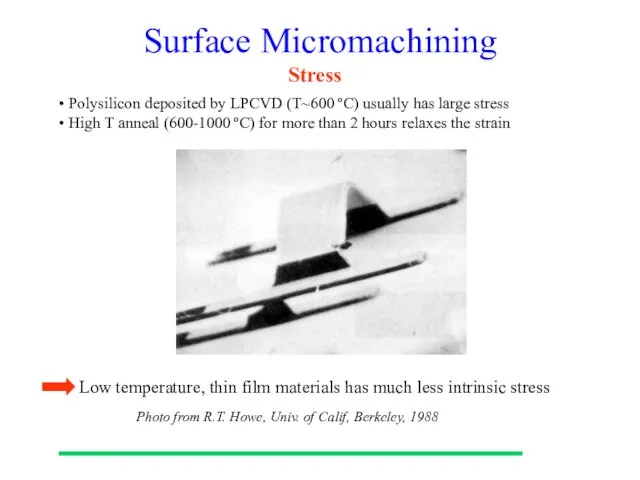
Surface Micromachining
Polysilicon deposited by LPCVD (T~600 ºC) usually has large
Surface Micromachining
Polysilicon deposited by LPCVD (T~600 ºC) usually has large
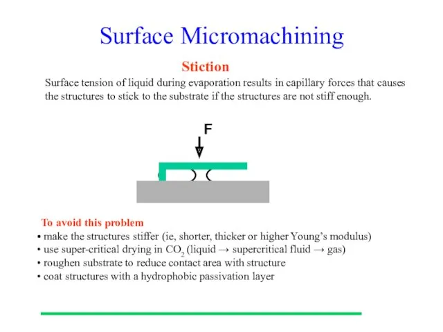
Surface Micromachining
Surface tension of liquid during evaporation results in capillary forces
Surface Micromachining
Surface tension of liquid during evaporation results in capillary forces
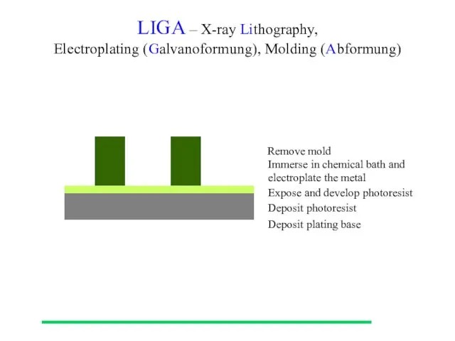
LIGA – X-ray Lithography,
Electroplating (Galvanoformung), Molding (Abformung)
Deposit plating base
Deposit photoresist
Expose
LIGA – X-ray Lithography,
Electroplating (Galvanoformung), Molding (Abformung)
Deposit plating base
Deposit photoresist
Expose
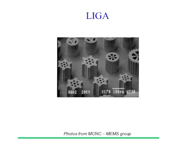
LIGA
Photos from MCNC – MEMS group
LIGA
Photos from MCNC – MEMS group
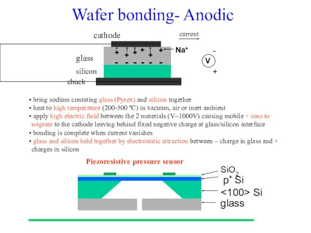
Wafer bonding- Anodic
bring sodium contating glass (Pyrex) and silicon together
Wafer bonding- Anodic
bring sodium contating glass (Pyrex) and silicon together
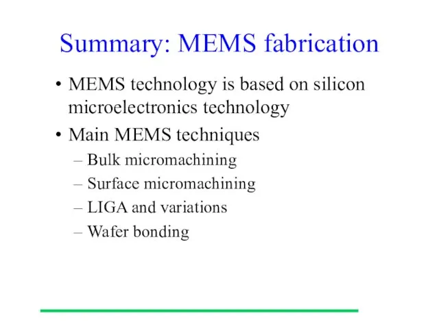
Summary: MEMS fabrication
MEMS technology is based on silicon microelectronics technology
Main MEMS
Summary: MEMS fabrication
MEMS technology is based on silicon microelectronics technology
Main MEMS
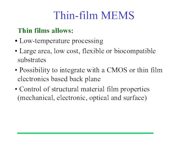
Thin-film MEMS
Thin films allows:
Low-temperature processing
Large area, low cost, flexible
Thin-film MEMS
Thin films allows:
Low-temperature processing
Large area, low cost, flexible
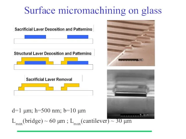
d=1 μm; h=500 nm; b=10 μm
Lmax(bridge) ~ 60 μm ; Lmax(cantilever)
d=1 μm; h=500 nm; b=10 μm
Lmax(bridge) ~ 60 μm ; Lmax(cantilever)
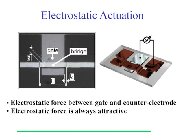
Electrostatic force between gate and counter-electrode
Electrostatic force is always
Electrostatic force between gate and counter-electrode
Electrostatic force is always
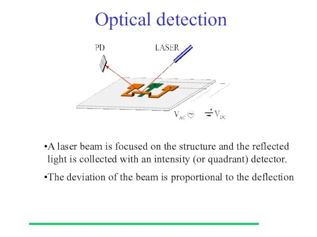
A laser beam is focused on the structure and the reflected
A laser beam is focused on the structure and the reflected
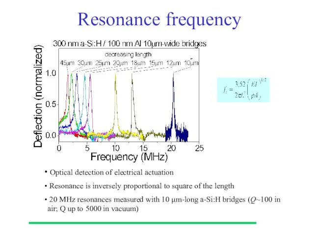
Optical detection of electrical actuation
Resonance is inversely proportional to
Optical detection of electrical actuation
Resonance is inversely proportional to
 Презентация 8 Марта - праздник мам!
 Квартирная электропроводка. 8 класс
 Игры и игровые упражнения в логопедической работе с детьми. Развитие мелкой моторики рук
 Основы технической диагностики. Общие требования по безопасности промышленных объектов, установленные законами РФ
 Методы изучения генетики человека
 Итоги о проделанной работе районного методического объединения воспитателей дошкольных образовательных организаций
 Транзисторы и тиристоры
 Великдень. Куличи на Пасху
 Презентация Разделение неоднородный смесей.
 Ырғақ бұзылыстары
 Организация деятельности приёмной Апатитского городского суда
 Коллективный проект Перемена
 Презентация к уроку технология 4 класс с творческими проектами детей. Тема Дизайн календаря
 Космический аналог ядерной угрозы
 Культура Беларуси в XIV - первой половине XVI в. Образование белорусской народности. Происхождение названия Белая Русь
 Общая психология
 Світове господарство та тенденції його розвитку
 Землеройно-транспортные машины
 тренажёры Диск
 Зелёный ад
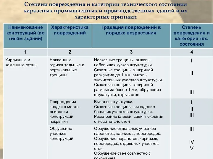 Степени повреждения и категории технического состояния промышленных и производственных зданий и их характерные признаки
 Ғылым тілі
 Моделирование и формализация. Система управления базами данных
 образец
 Методические разработки уроков
 Краткий тезаурус по ВВЭР-1200
 На юге Европы. Греция и Италия
 Парентеральный путь введения лекарственных средств в организм