- Мікропроцесорна техніка PSoC Creator 4.2 Designing with PSoC 3/5. (Лекція 5)

Содержание
- 2. PSoC@3/5 IDAC8 PSoC Creator 4.2 Designing with PSoC 3/5
- 3. Модулі PSoC@3/5
- 4. Модулі PSoC@3/5
- 5. IDAC8 Block Diagram IDAC8
- 6. Lab_5 IDAC8
- 7. IDAC8
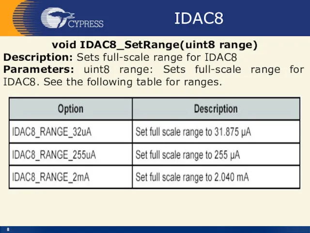
- 8. IDAC8 void IDAC8_SetRange(uint8 range) Description: Sets full-scale range for IDAC8 Parameters: uint8 range: Sets full-scale range
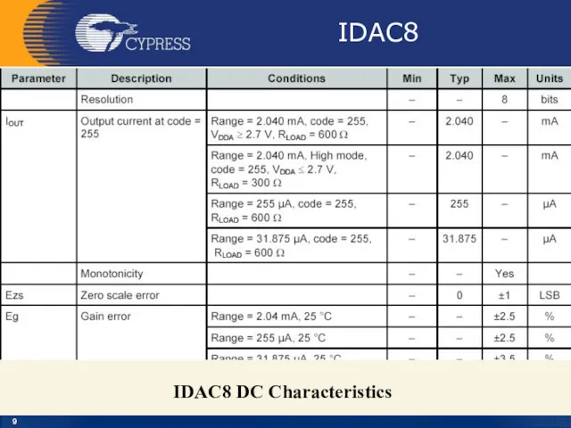
- 9. IDAC8 IDAC8 DC Characteristics
- 10. IDAC8 Iout – Analog The Iout terminal, the terminal on the right side of the symbol,
- 11. IDAC8 ipolarity – Input* The ipolarity input is an optional signal input pin. This pin can
- 12. IDAC8
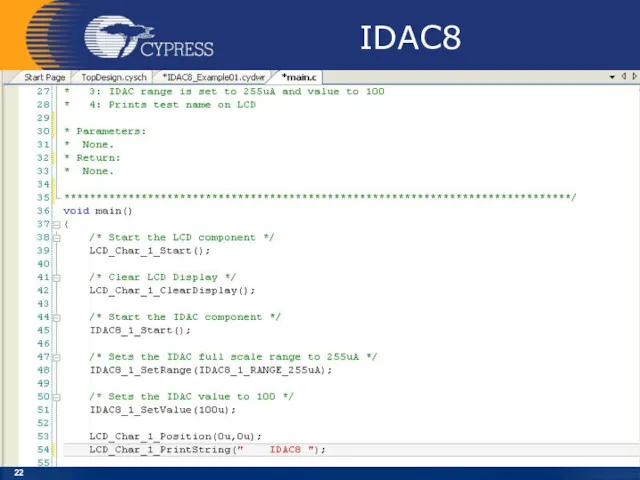
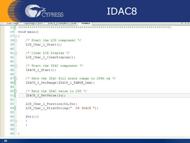
- 13. IDAC8 Follow the below steps to do this: The Lab already has the LCD Character component
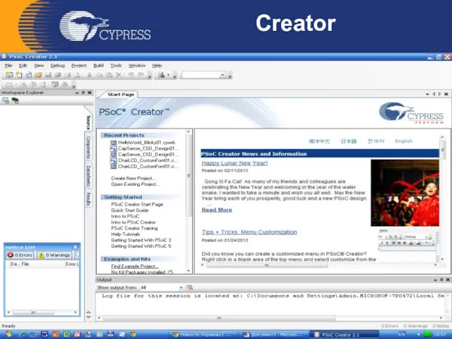
- 14. Creator
- 15. File – New - Projekt
- 16. Empty PSoC 3 Design
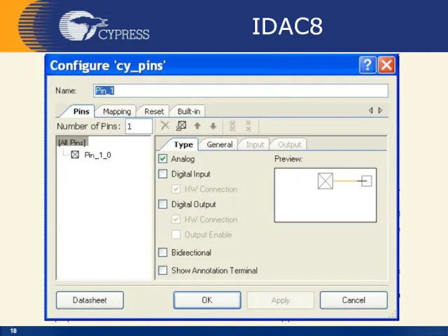
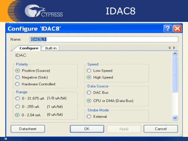
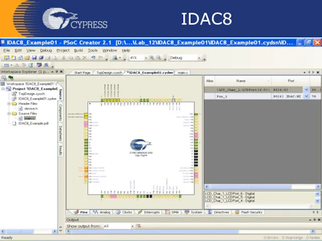
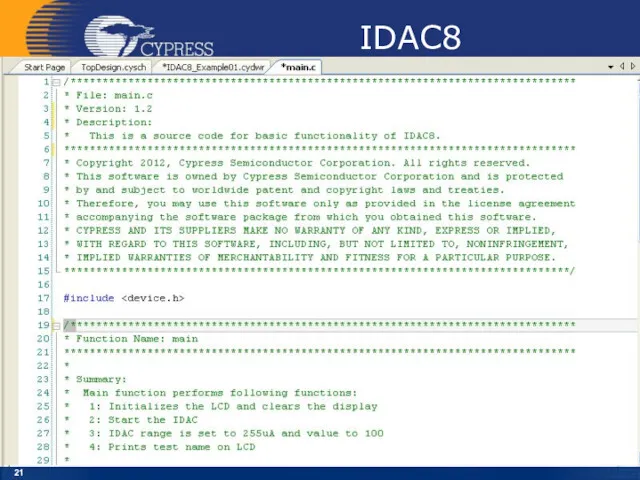
- 17. IDAC8
- 18. IDAC8
- 19. IDAC8
- 20. IDAC8
- 21. IDAC8
- 22. IDAC8
- 23. IDAC8
- 24. IDAC8 Overview: Activate and use the IDAC8 on the DVK board and output the results to
- 25. IDAC8 Зняти вольт-амперну характеристику напівпровідникового діода
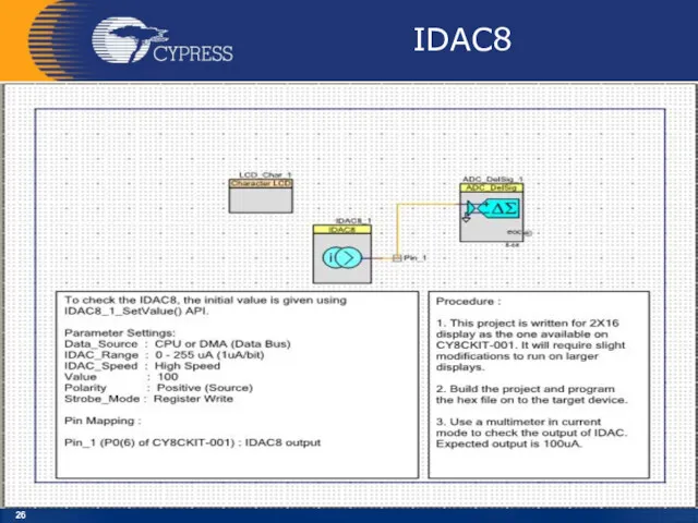
- 26. IDAC8
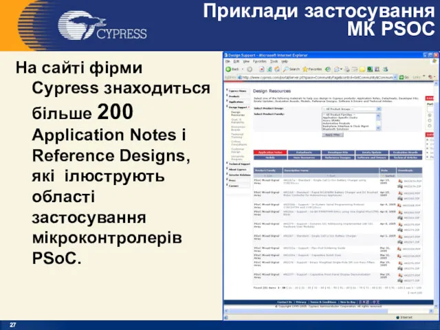
- 27. Приклади застосування МК PSOC На сайті фірми Cypress знаходиться більше 200 Application Notes і Reference Designs,
- 29. Скачать презентацию
PSoC@3/5
IDAC8
PSoC Creator 4.2
Designing with PSoC 3/5
PSoC@3/5
IDAC8
PSoC Creator 4.2
Designing with PSoC 3/5
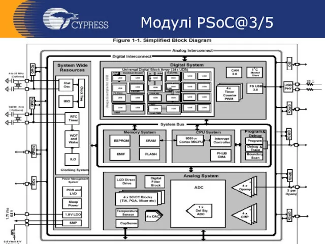
Модулі PSoC@3/5
Модулі PSoC@3/5
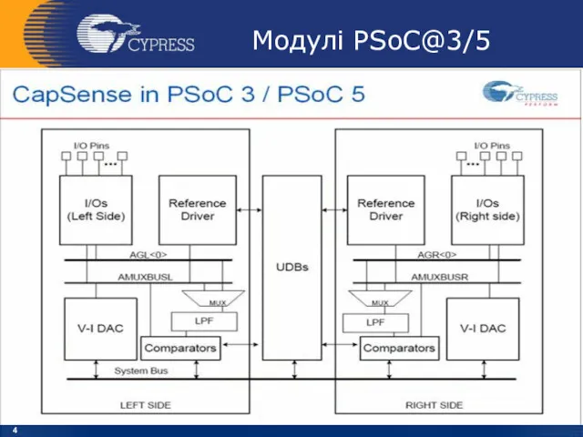
Модулі PSoC@3/5
Модулі PSoC@3/5
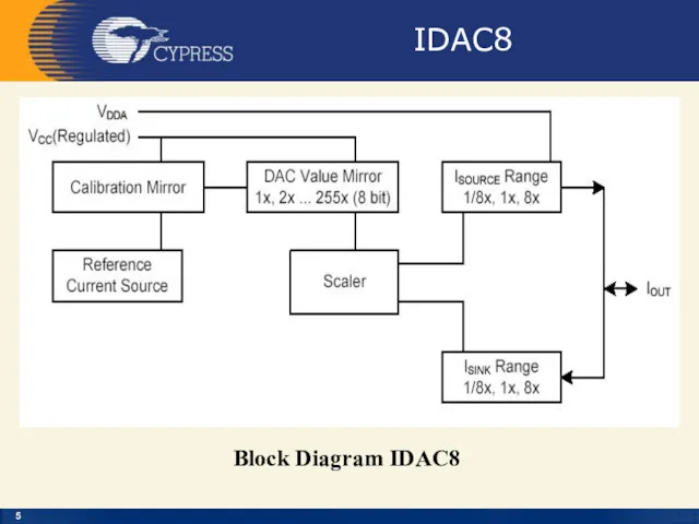
IDAC8
Block Diagram IDAC8
IDAC8
Block Diagram IDAC8
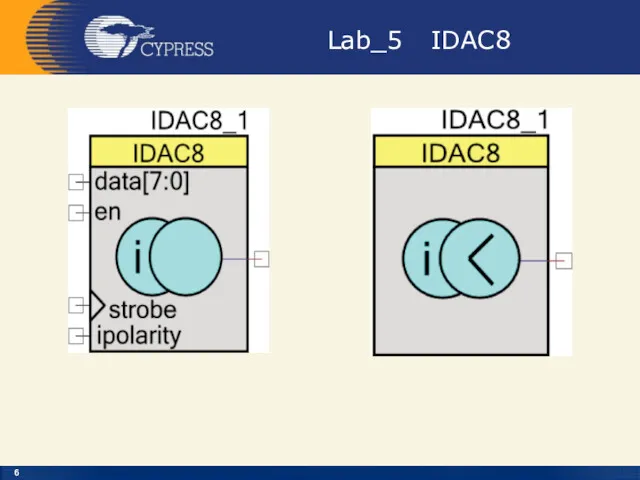
Lab_5 IDAC8
Lab_5 IDAC8
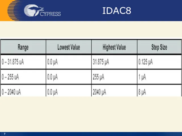
IDAC8
IDAC8
IDAC8
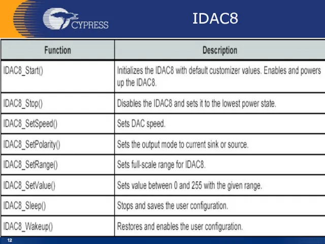
void IDAC8_SetRange(uint8 range)
Description: Sets full-scale range for IDAC8
Parameters: uint8 range:
IDAC8
void IDAC8_SetRange(uint8 range)
Description: Sets full-scale range for IDAC8
Parameters: uint8 range:
IDAC8
IDAC8 DC Characteristics
IDAC8
IDAC8 DC Characteristics
IDAC8
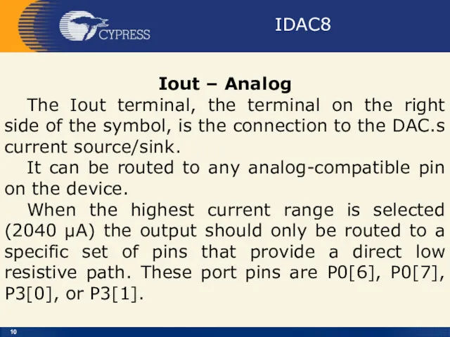
Iout – Analog
The Iout terminal, the terminal on the right
IDAC8
Iout – Analog
The Iout terminal, the terminal on the right
IDAC8
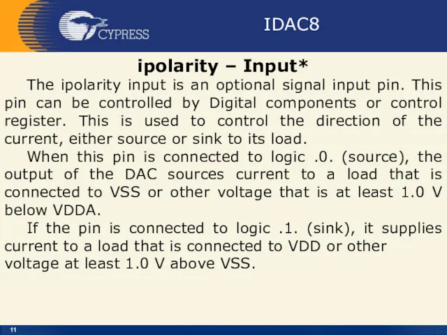
ipolarity – Input*
The ipolarity input is an optional signal input
IDAC8
ipolarity – Input*
The ipolarity input is an optional signal input
IDAC8
IDAC8
IDAC8
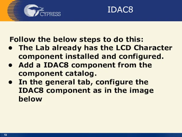
Follow the below steps to do this:
The Lab already has
IDAC8
Follow the below steps to do this:
The Lab already has
Creator
Creator
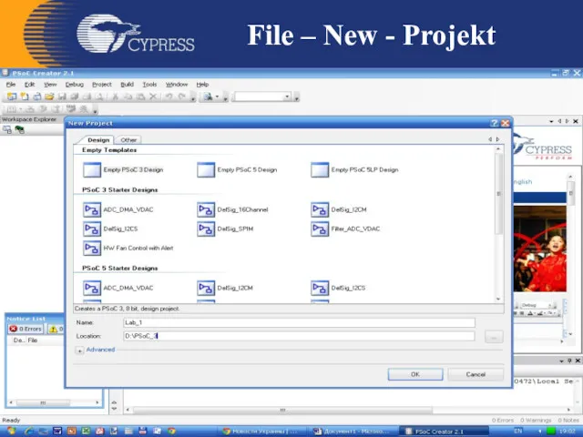
File – New - Projekt
File – New - Projekt
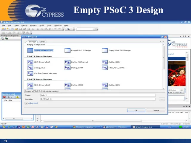
Empty PSoC 3 Design
Empty PSoC 3 Design
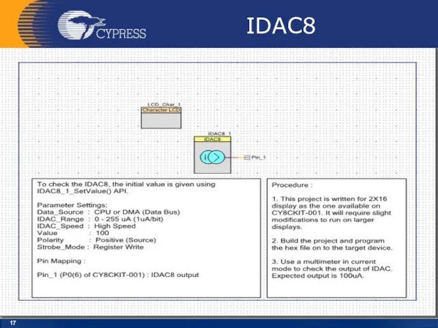
IDAC8
IDAC8
IDAC8
IDAC8
IDAC8
IDAC8
IDAC8
IDAC8
IDAC8
IDAC8
IDAC8
IDAC8
IDAC8
IDAC8
IDAC8
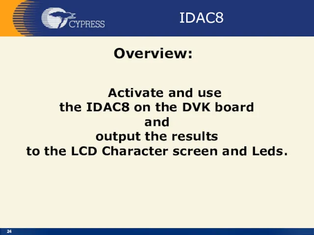
Overview:
Activate and use
the IDAC8 on the DVK board
and
IDAC8
Overview:
Activate and use
the IDAC8 on the DVK board
and
IDAC8
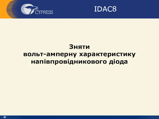
Зняти
вольт-амперну характеристику
напівпровідникового діода
IDAC8
Зняти
вольт-амперну характеристику
напівпровідникового діода
IDAC8
IDAC8
Приклади застосування
МК PSOC
На сайті фірми Cypress знаходиться більше 200 Application
Приклади застосування
МК PSOC
На сайті фірми Cypress знаходиться більше 200 Application
 Христианская семья
 Инновации в мире технологий
 Повышение эффективности технического обеспечения молочно-товарного Комплекса в СПК Гожа Гродненского района
 Аксиомы стереометрии и их следствия
 Великдень. Куличи на Пасху
 Карамель. Формування споживних властивостей карамелі. Класифікація і формування асортименту карамелі
 Система менеджмента безопасности движения
 Основы VBA. Арифметические операторы VBA
 Лидеры и элиты в политической жизни
 Мейоз. Механизм мейоза
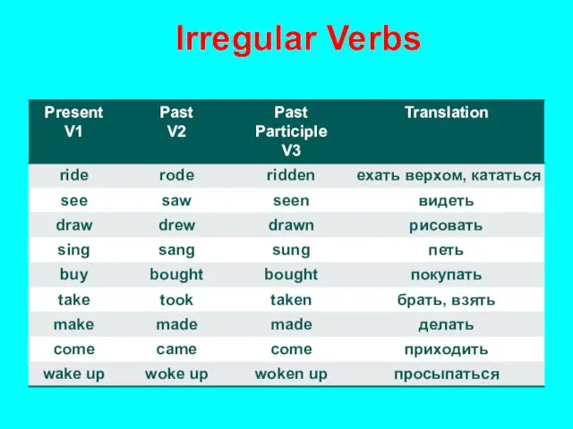 Irregular Verbs
 Правила обращения за региональной социальной доплатой к пенсии, порядок ее установления, выплаты и пересмотра ее размера
 Дробные выражения. Устный счет
 Эпидемиология и профилактика сибирской язвы
 Биологическое и социальное в структуре личности
 Ударение
 Презентация по творчеству С.Есенина
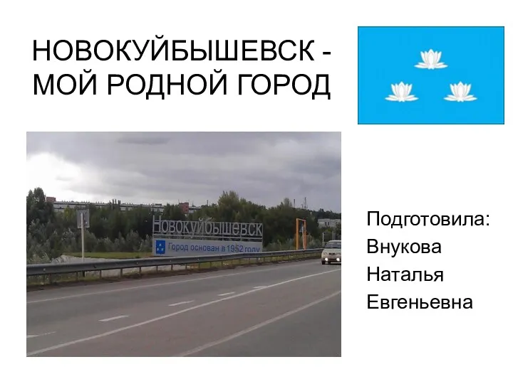 Презентация для детей Новокуйбышевск - мой родной город
 Неделя профилактики употребления алкоголя. Классный час в 5-Н классе – Альтернатива вредным привычкам
 Охранно - пожарная сигнализация. Виды сигнализаций
 Технология изготовления металлического мангала
 Ми ісіктері мен инфекциялары кезіндегі психикалық бұзылыстар
 День матери
 Государственная идеология как социально-политический феномен
 Компьютер – помощник и друг
 активированный уголь
 Прорастание семян
 Приёмные антенны и их параметры. Лекция № 7. АФУ