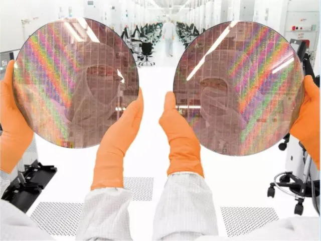
- Semiconductor technology

Содержание
- 3. This is the position of the bandgap in a semiconductor crystal - between the valence band
- 4. In the band structure of semiconductors, there is such a parameter as the Fermi level, which
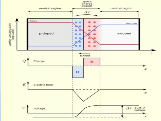
- 5. The most interesting processes begin when semiconductors of p- and n-types are arranged with each other.
- 7. The transistor has a relatively simple design, but at the same time there are some difficulties
- 9. Скачать презентацию
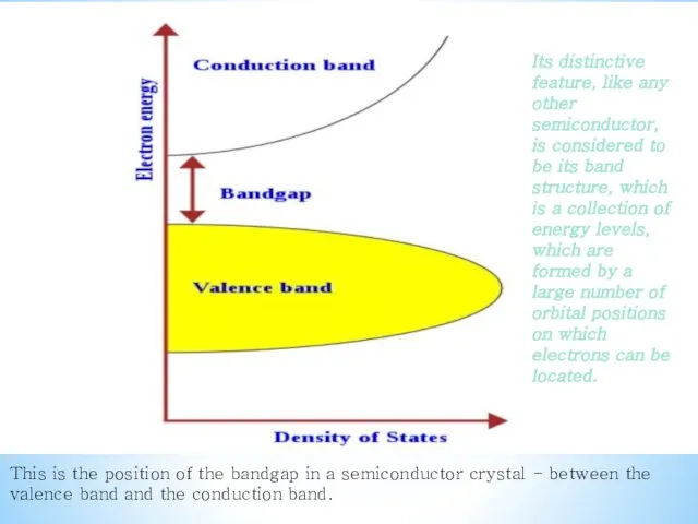
This is the position of the bandgap in a semiconductor crystal
This is the position of the bandgap in a semiconductor crystal
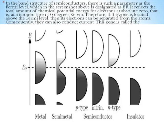
In the band structure of semiconductors, there is such a parameter
In the band structure of semiconductors, there is such a parameter
The most interesting processes begin when semiconductors of p- and n-types
The most interesting processes begin when semiconductors of p- and n-types
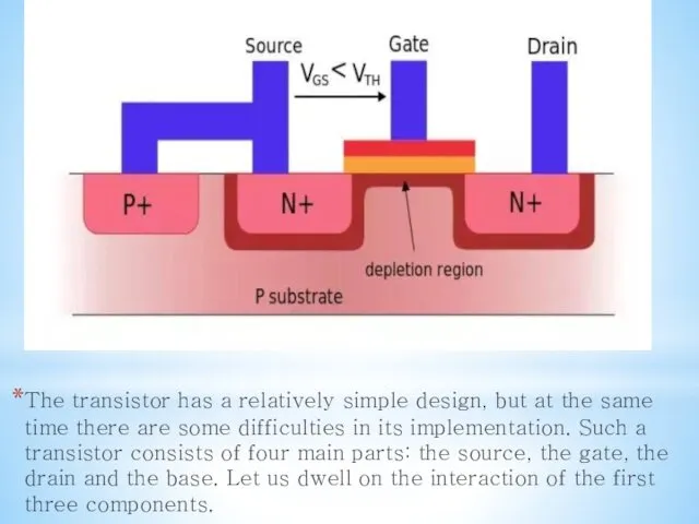
The transistor has a relatively simple design, but at the same
The transistor has a relatively simple design, but at the same
 Оборудование используемое для искривления ствола скважин
 Печатные формы высокой печати
 Эффективные маркетинговые коммуникации в менеджменте
 Кодирование звука. Временная дискретизация
 Методическая разработка
 Безопасное поведение детей в сети
 Подготовка поверхности под улучшенную окраску. Сплошное шпатлевание поверхности под улучшенную окраску
 Викторина по деятельности К.Д. Ушинского
 Сказочный зверинец в Санкт-Петербурге (Конные памятники)
 Духовно-нравственное воспитание
 Філософія Стародавніх Китаю та Індії. Лекція 2
 Erntedankfest. День благодарения
 ОГЭ тренажер
 Государственные должности и должности государственной службы
 Благодарность, смысл жизни. Сочинение на ОГЭ-2017. (Задание 15.3)
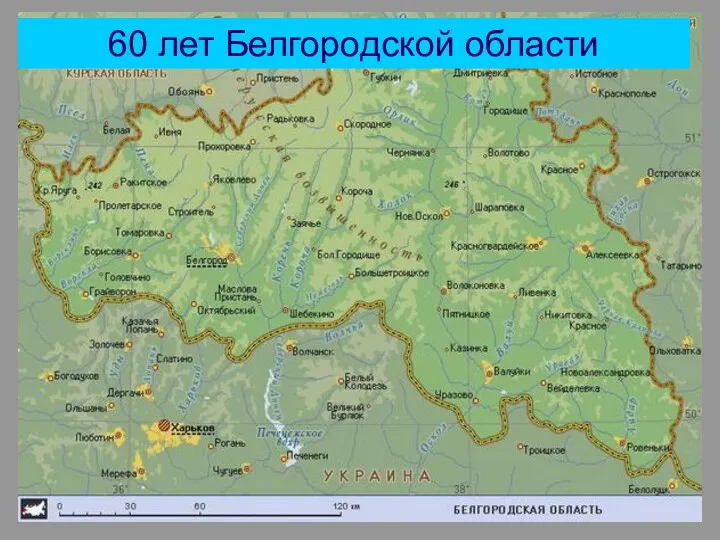 60 лет Белгородской области
 Сравнение, сложение и вычитание дробей с разными знаменателями
 Синдром Вильсона - Коновалова
 Места обитания животных
 Вариативные программы обучения
 Падение Рима
 Ткань. Виды ткани.
 Правила технической эксплуатации, инструкция по сигнализации железных дорог РФ
 Развивающие образовательные технологии и системно-деятельностный подход в обучении школьников на уроках иностранного языка
 Олимпийские игры Сочи 2014
 Понятие системы права. Отрасли права. Публичное и частное право
 Зеленая дорога детства
 Семейное хобби