- Microelectronic front-end of receivers for wireless systems

Содержание
- 2. Wireless communication systems Cell phones (GSM, WCDMA), Bluetooth, Wireless local area network (WLAN), Digital enhanced cordless
- 3. Transceiver quadratur modulator Input signal Heterodyne Mixers Output signals
- 4. Receiver architecture RF bandpass filter (RF BPF), low noise amplifier (LNA) I/Q channels: 2 mixers, local
- 5. Transceiver architecture
- 6. Signals in the receiver interface Let us consider an input signal as Signals from mixers are
- 7. Advantages of zero IF receiver High-performance off-chip bandpass filter in the IF part of receivers can
- 8. General requirements for receivers
- 9. General requirements for multistandard receivers
- 10. Non-linear parameters «характеристические точки мощности интермодуляционных искажений N–ого порядка» IIPN (N-th order Intermodulation Intercept Point). N
- 11. IIP3 Выходной сигнал В этом случае IIP3 – это мощность входного сигнала на одной из частот,
- 12. Low-Noise Amplifier for Receiver Согласование по мощности в узкой полосе частот осуществляется Lg, в то время
- 13. Low-Noise Amplifier for Multistandard Receiver (а) (b)
- 14. Mixers for Receiver (Multistandard Receiver) Эквивалентная схема преобразователя Гильберта по переменному току.
- 15. Voltage-Controlled Oscillator for Receiver Фазовые шумы, отстройка 100 кГц - 100 -110 дБ/Гц Типовой диапазон перестройки
- 16. Voltage-Controlled Oscillator for Multistandard Receiver
- 17. Filter Design: Some common features The order of filters is of 5th at least. The cut-off
- 18. Low-pass channel selected filter requirements
- 19. Conception Cascaded design allows implementation of high performance filters. Cascaded realizations are not optimal from a
- 20. Gm-C filter design a) CMOS transconductance amplifier design Cross-coupled stage Stage with degeneration Low-voltage stages: 2
- 21. Proposed transconductor circuit Input stage [1] Complete structure [2], [3]
- 22. b)Gm-C filter design Layout Structure of the filter [2], [3] Tuning system
- 23. Practical results Amplitude response Output spectrum Noise spectrum (simulation and experiment)
- 24. Filter characteristics
- 25. Current conveyor (CCII) based filter design An alternative way for the high-frequency filter realization is using
- 26. CCII and SC-integrators on its basis
- 27. a) Filter blocks Current conveyor [5] Voltage buffer [5] CMOS dummy switch
- 28. b) Filter structure The synthesized filter is based on the parasitic insensitive integrators [4]. The filter
- 29. Practical results Amplitude response Output spectrum Noise spectrum
- 30. Filter characteristics
- 31. Analog-to-Digital Converters Main types of ADC’s are - Parallel-flash (параллельный) - Successive Approximation (последовательных приближений) -
- 32. SWITCHED-CAPACITOR DELTA-SIGMA MODULATORS Advantages: - Wide dynamic range; - Low noise; - High linearity; - Low
- 33. First Order Delta-Sigma ADC Block Diagram
- 34. A representation of the first-order delta-sigma (ΔΣ) modulator DELTA-SIGMA MODULATOR SC implementation of first-order ΔΣ modulator
- 35. SIMULATION PROGRAMS OVERVIEW
- 36. A representation of the SC circuit by the set of linear differential equations in the nodal
- 37. SOLVING OF NONLINEAR CIRCUIT EQUATIONS where f(·) is a function describing nonlinear properties of elements. The
- 38. A. Capacitance nonlinearities Nonlinear properties of the each parasitic drain-bulk and source-bulk capacitors of MOS transistors
- 39. After two-dimensional Laplace transform the solution of the set is expressed as where U2k(0,s2), U2k(s1,0) are
- 40. B. Active elements nonlinearities The nonlinear DC characteristic of balanced amplifier can be approximated as following
- 41. The partial initial conditions are obtained from nodal analysis model given t1=0, t2=0, t3=0 respectively.
- 42. Implementation of second-order ΔΣ modulator The equivalent circuit of the second-order ΔΣ modulator SC part in
- 43. line 1 – results of behavioral simulation using Simulink, line 2 – gon=1 1/Ohm, ideal OpA,
- 44. Simulation results of second-order ΔΣ modulator for stray capacitor nonlinearities
- 45. Classification of Integrated Circuits ASIC – Application Specific IC MPIC – Mask Programmed IC UPIC –
- 46. Typical FPAA Block Diagram Input/Output Blocks – For Antialiasing and Smoothing purposes CAB (Configurable Analog Block
- 47. Main FPAA Vendors Anadigm – specialized on switched capacitor ICs Motorola – specialized on switched capacitor
- 48. Basic features of FPAA’s AN10E40, MPAA020,TRAC020LH and ispPAC20 *) SC – switched capacitor circuit CT –
- 49. Anadigm’s CAB Block Diagram
- 50. Sample-and-Hold Adder - Subtractor block Integrator Comparator First-order DAC FPAA implementation of Delta-Sigma Modulator (Anadigm Designer
- 51. Computer Simulation Initial Conditions Clock Frequency 1MHz Test signal Frequency 5kHz Amplitude of test signal 2V
- 52. Voltage oscillogramms: output of Sample-and-Hold (Magenta), output of Delta-Sigma Modulator (Yellow), output of integrator (Blue) *Anadigm
- 53. Switched Capacitor Schematic of 1-st Order Delta-Sigma Modulator based on FPAA
- 54. Measuring Scheme
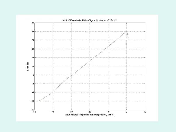
- 55. Output signal spectrum of 1-st order Delta-Sigma Modulator with 1Mhz clock frequency
- 56. Output signal spectrum of 1-st order Delta-Sigma Modulator with 250kHz clock frequency
- 58. Conclusions 1.Proposed approaches are perspective and can be used for the CMOS design of selective circuits
- 59. CONCLUSIONS 4. Simulation program has been proposed for analysis of oversampled switched-capacitor Delta-Sigma modulator. 5. The
- 60. CONCLUSIONS Delta-Sigma modulator has been realized on a basis of FPAA Anadigm AN10E40; For the proposed
- 62. Скачать презентацию
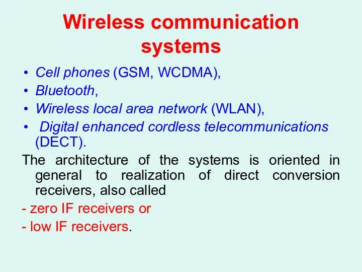
Wireless communication systems
Cell phones (GSM, WCDMA),
Bluetooth,
Wireless local area network
Wireless communication systems
Cell phones (GSM, WCDMA),
Bluetooth,
Wireless local area network
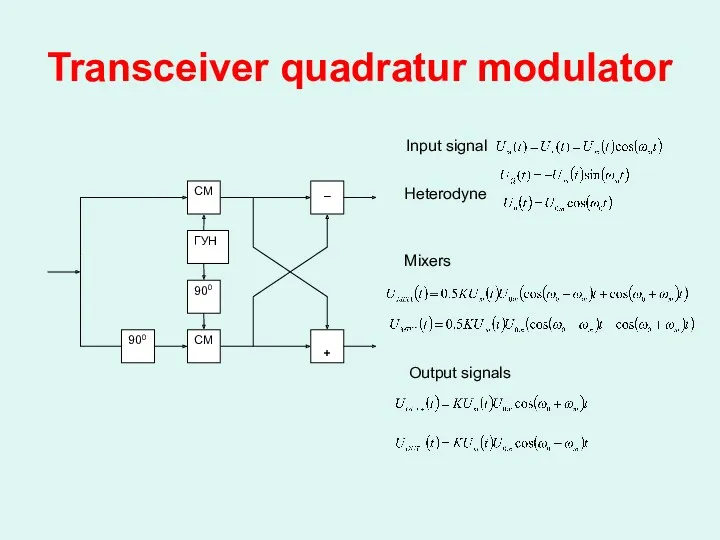
Transceiver quadratur modulator
Input signal
Heterodyne
Mixers
Output signals
Transceiver quadratur modulator
Input signal
Heterodyne
Mixers
Output signals
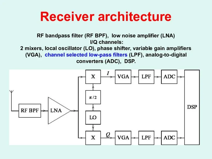
Receiver architecture
RF bandpass filter (RF BPF), low noise amplifier (LNA) I/Q
Receiver architecture RF bandpass filter (RF BPF), low noise amplifier (LNA) I/Q
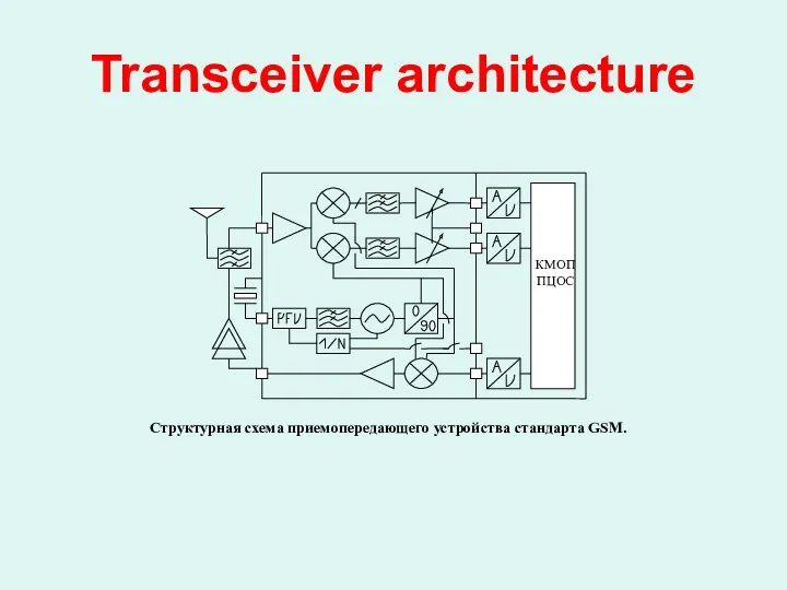
Transceiver architecture
Transceiver architecture
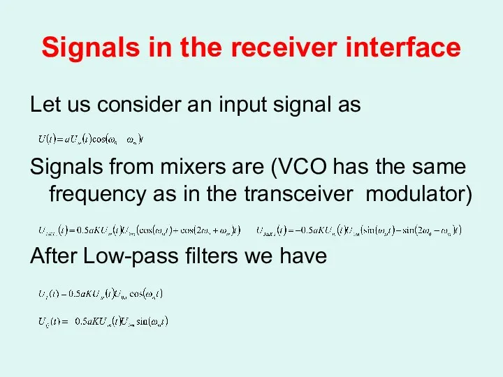
Signals in the receiver interface
Let us consider an input signal as
Signals
Signals in the receiver interface
Let us consider an input signal as
Signals
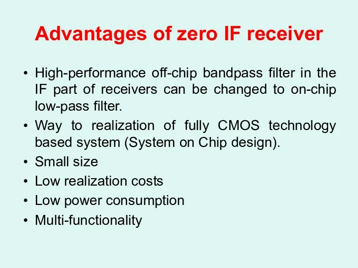
Advantages of zero IF receiver
High-performance off-chip bandpass filter in the IF
Advantages of zero IF receiver
High-performance off-chip bandpass filter in the IF
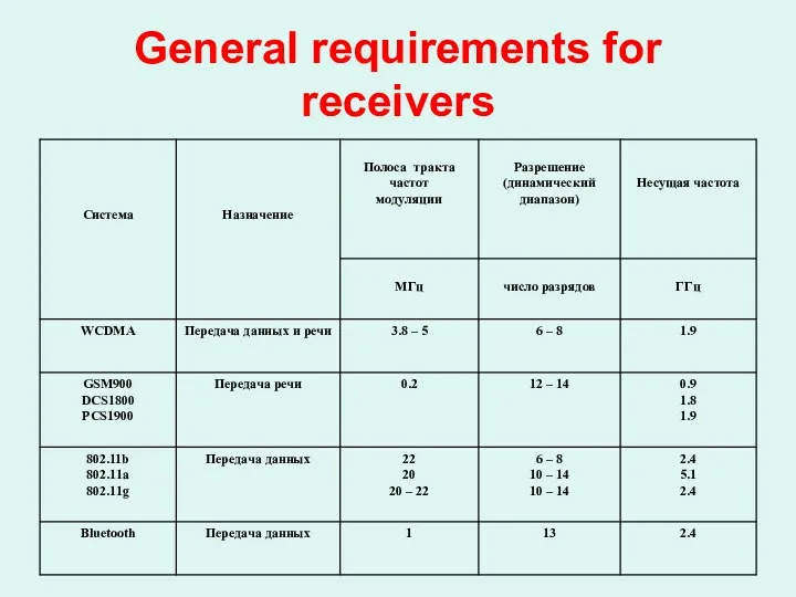
General requirements for receivers
General requirements for receivers
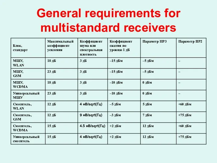
General requirements for multistandard receivers
General requirements for multistandard receivers
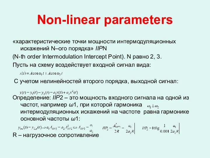
Non-linear parameters
«характеристические точки мощности интермодуляционных искажений N–ого порядка» IIPN
(N-th order
Non-linear parameters
«характеристические точки мощности интермодуляционных искажений N–ого порядка» IIPN
(N-th order
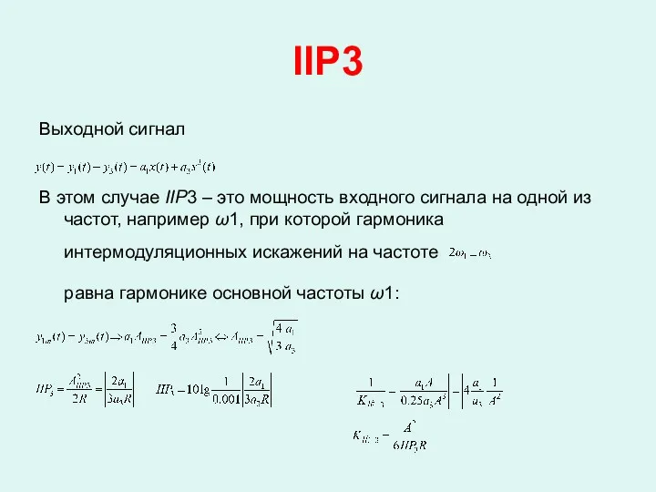
IIP3
Выходной сигнал
В этом случае IIP3 – это мощность входного сигнала на
IIP3
Выходной сигнал
В этом случае IIP3 – это мощность входного сигнала на
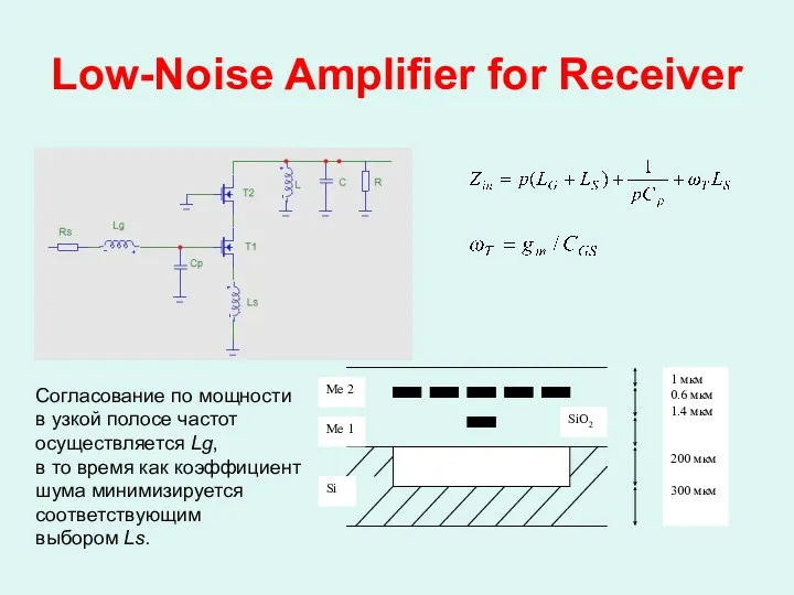
Low-Noise Amplifier for Receiver
Согласование по мощности
в узкой полосе частот
осуществляется
Low-Noise Amplifier for Receiver
Согласование по мощности
в узкой полосе частот
осуществляется
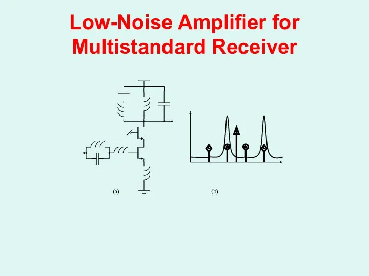
Low-Noise Amplifier for Multistandard Receiver
(а)
(b)
Low-Noise Amplifier for Multistandard Receiver
(а)
(b)
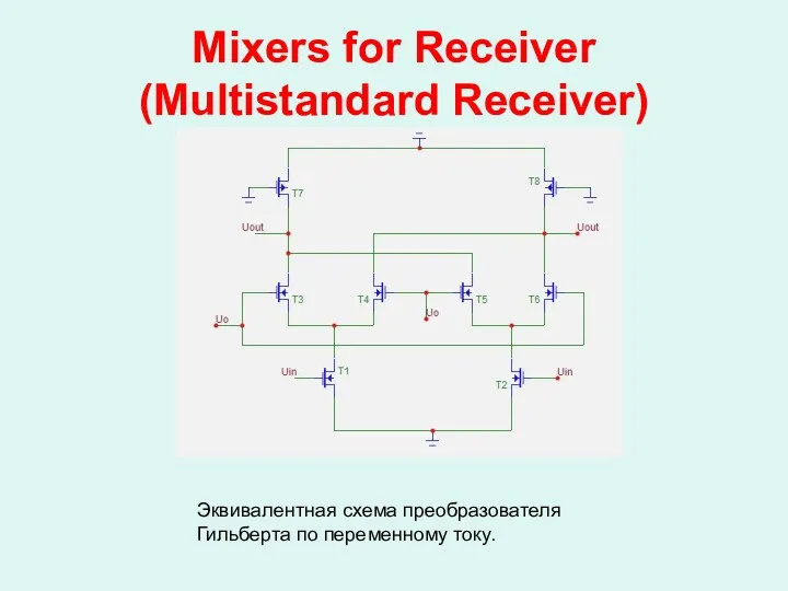
Mixers for Receiver (Multistandard Receiver)
Эквивалентная схема преобразователя
Гильберта по переменному току.
Mixers for Receiver (Multistandard Receiver)
Эквивалентная схема преобразователя
Гильберта по переменному току.
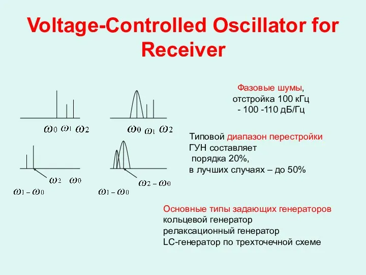
Voltage-Controlled Oscillator for Receiver
Фазовые шумы,
отстройка 100 кГц
- 100 -110
Voltage-Controlled Oscillator for Receiver
Фазовые шумы,
отстройка 100 кГц
- 100 -110
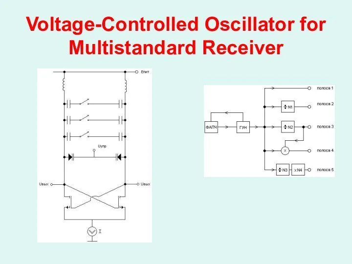
Voltage-Controlled Oscillator for Multistandard Receiver
Voltage-Controlled Oscillator for Multistandard Receiver
Filter Design:
Some common features
The order of filters is of 5th at
Filter Design:
Some common features
The order of filters is of 5th at
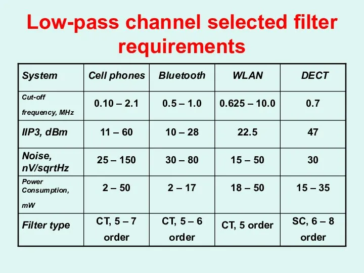
Low-pass channel selected filter requirements
Low-pass channel selected filter requirements
Conception
Cascaded design allows implementation of high performance filters.
Cascaded realizations are
Conception
Cascaded design allows implementation of high performance filters.
Cascaded realizations are
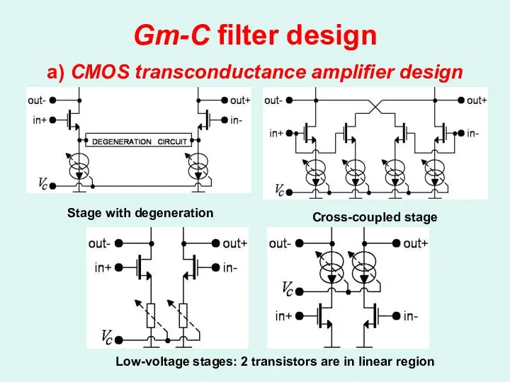
Gm-C filter design
a) CMOS transconductance amplifier design
Cross-coupled stage
Stage with degeneration
Low-voltage
Gm-C filter design
a) CMOS transconductance amplifier design
Cross-coupled stage
Stage with degeneration
Low-voltage
![Proposed transconductor circuit Input stage [1] Complete structure [2], [3]](/_ipx/f_webp&q_80&fit_contain&s_1440x1080/imagesDir/jpg/203703/slide-20.jpg)
Proposed transconductor circuit
Input stage [1]
Complete structure [2], [3]
Proposed transconductor circuit
Input stage [1]
Complete structure [2], [3]
![b)Gm-C filter design Layout Structure of the filter [2], [3] Tuning system](/_ipx/f_webp&q_80&fit_contain&s_1440x1080/imagesDir/jpg/203703/slide-21.jpg)
b)Gm-C filter design
Layout
Structure of the filter [2], [3]
Tuning system
b)Gm-C filter design
Layout
Structure of the filter [2], [3]
Tuning system
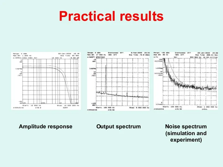
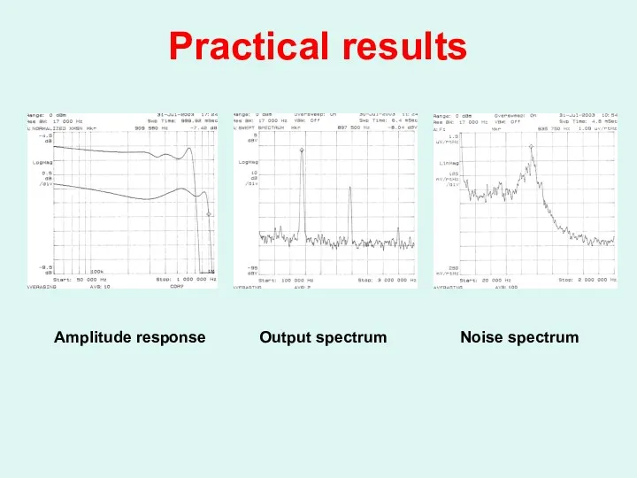
Practical results
Amplitude response
Output spectrum
Noise spectrum
(simulation and
experiment)
Practical results
Amplitude response
Output spectrum
Noise spectrum
(simulation and
experiment)
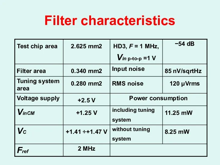
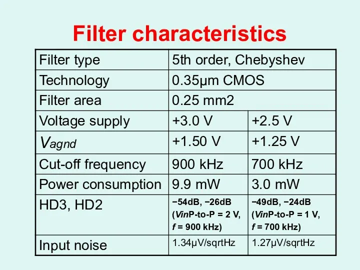
Filter characteristics
Filter characteristics
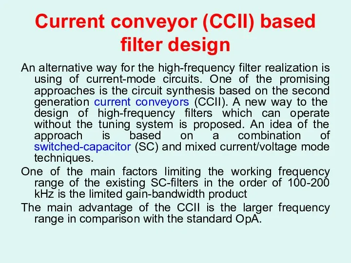
Current conveyor (CCII) based filter design
An alternative way for the
Current conveyor (CCII) based filter design
An alternative way for the
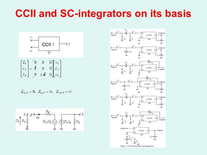
CCII and SC-integrators on its basis
CCII and SC-integrators on its basis
![a) Filter blocks Current conveyor [5] Voltage buffer [5] CMOS dummy switch](/_ipx/f_webp&q_80&fit_contain&s_1440x1080/imagesDir/jpg/203703/slide-26.jpg)
a) Filter blocks
Current conveyor [5]
Voltage buffer [5]
CMOS dummy switch
a) Filter blocks
Current conveyor [5]
Voltage buffer [5]
CMOS dummy switch
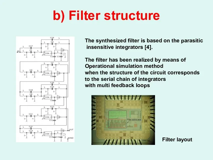
b) Filter structure
The synthesized filter is based on the parasitic
insensitive
b) Filter structure
The synthesized filter is based on the parasitic
insensitive
Practical results
Amplitude response
Output spectrum
Noise spectrum
Practical results
Amplitude response
Output spectrum
Noise spectrum
Filter characteristics
Filter characteristics
Analog-to-Digital Converters
Main types of ADC’s are
- Parallel-flash (параллельный)
- Successive Approximation (последовательных
Analog-to-Digital Converters
Main types of ADC’s are
- Parallel-flash (параллельный)
- Successive Approximation (последовательных
SWITCHED-CAPACITOR DELTA-SIGMA MODULATORS
Advantages:
- Wide dynamic range;
- Low noise;
- High linearity;
- Low
SWITCHED-CAPACITOR DELTA-SIGMA MODULATORS Advantages: - Wide dynamic range; - Low noise; - High linearity; - Low
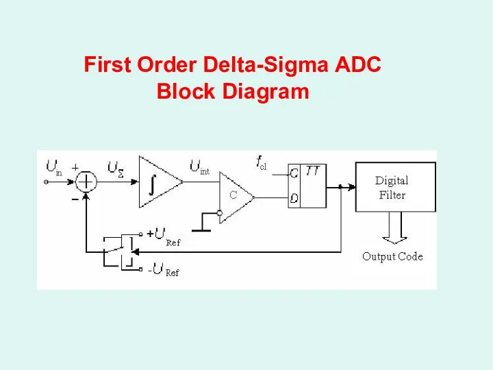
First Order Delta-Sigma ADC Block Diagram
First Order Delta-Sigma ADC Block Diagram
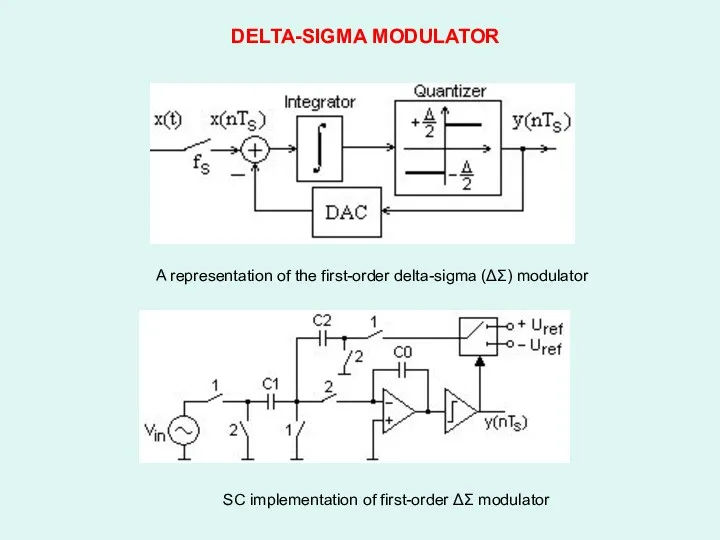
A representation of the first-order delta-sigma (ΔΣ) modulator
DELTA-SIGMA MODULATOR
SC implementation of
A representation of the first-order delta-sigma (ΔΣ) modulator
DELTA-SIGMA MODULATOR
SC implementation of
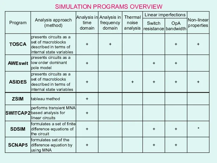
SIMULATION PROGRAMS OVERVIEW
SIMULATION PROGRAMS OVERVIEW
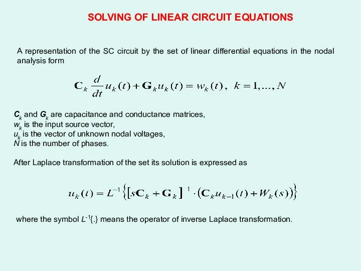
A representation of the SC circuit by the set of linear
A representation of the SC circuit by the set of linear
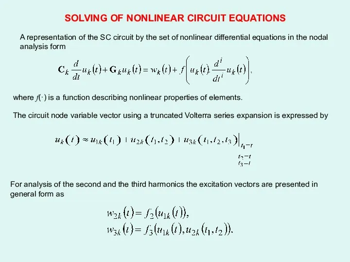
SOLVING OF NONLINEAR CIRCUIT EQUATIONS
where f(·) is a function describing nonlinear
SOLVING OF NONLINEAR CIRCUIT EQUATIONS
where f(·) is a function describing nonlinear
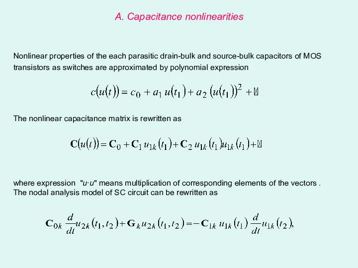
A. Capacitance nonlinearities
Nonlinear properties of the each parasitic drain-bulk and source-bulk
A. Capacitance nonlinearities
Nonlinear properties of the each parasitic drain-bulk and source-bulk
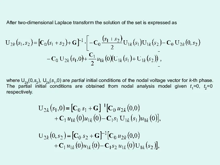
After two-dimensional Laplace transform the solution of the set is expressed
After two-dimensional Laplace transform the solution of the set is expressed
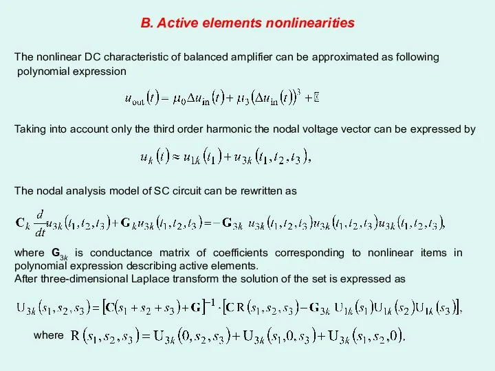
B. Active elements nonlinearities
The nonlinear DC characteristic of balanced amplifier can
B. Active elements nonlinearities
The nonlinear DC characteristic of balanced amplifier can
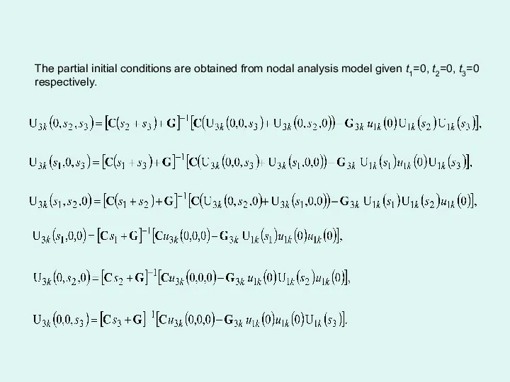
The partial initial conditions are obtained from nodal analysis model given
The partial initial conditions are obtained from nodal analysis model given
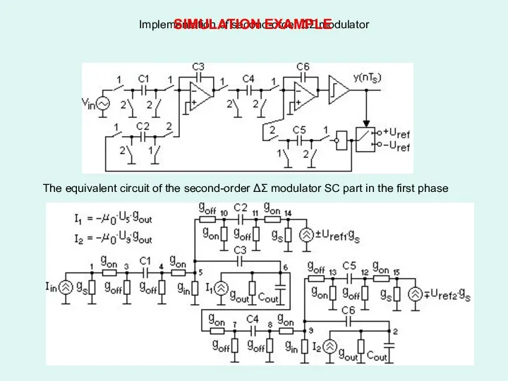
Implementation of second-order ΔΣ modulator
The equivalent circuit of the second-order ΔΣ
Implementation of second-order ΔΣ modulator
The equivalent circuit of the second-order ΔΣ
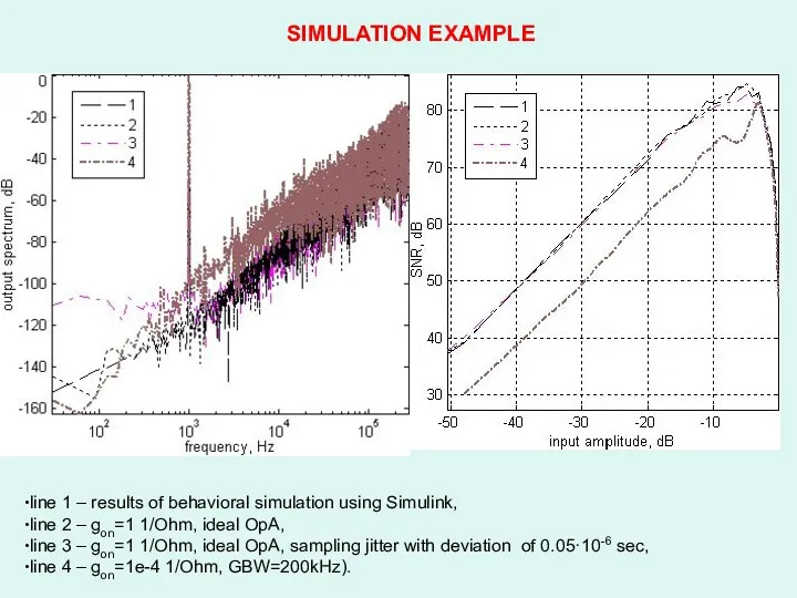
line 1 – results of behavioral simulation using Simulink,
line 2
line 1 – results of behavioral simulation using Simulink,
line 2
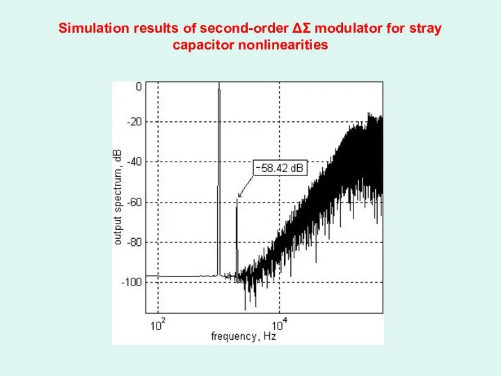
Simulation results of second-order ΔΣ modulator for stray capacitor nonlinearities
Simulation results of second-order ΔΣ modulator for stray capacitor nonlinearities
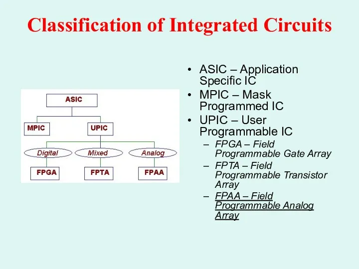
Classification of Integrated Circuits
ASIC – Application Specific IC
MPIC – Mask Programmed
Classification of Integrated Circuits
ASIC – Application Specific IC
MPIC – Mask Programmed
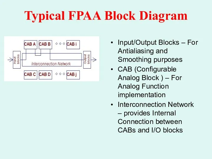
Typical FPAA Block Diagram
Input/Output Blocks – For Antialiasing and Smoothing purposes
CAB
Typical FPAA Block Diagram
Input/Output Blocks – For Antialiasing and Smoothing purposes
CAB
Main FPAA Vendors
Anadigm – specialized on switched capacitor ICs
Motorola –
Main FPAA Vendors
Anadigm – specialized on switched capacitor ICs
Motorola –
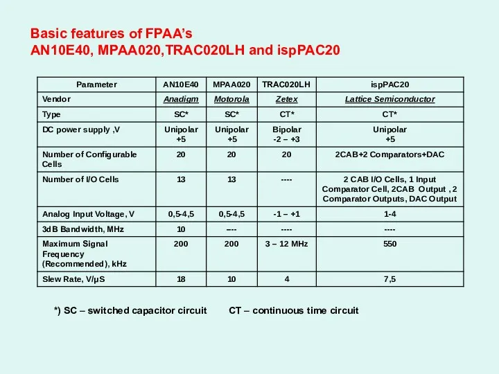
Basic features of FPAA’s
AN10E40, MPAA020,TRAC020LH and ispPAC20
*) SC – switched capacitor
AN10E40, MPAA020,TRAC020LH and ispPAC20
*) SC – switched capacitor
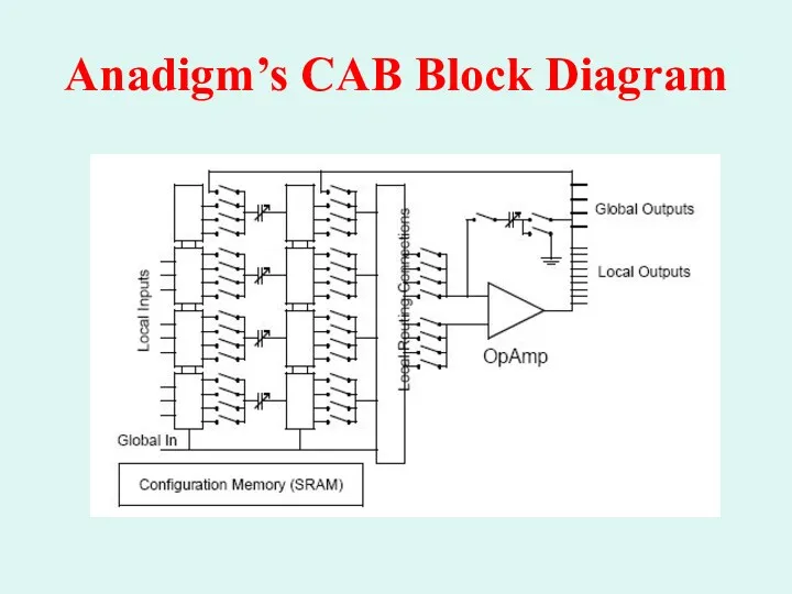
Anadigm’s CAB Block Diagram
Anadigm’s CAB Block Diagram
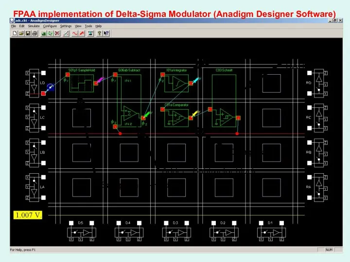
Sample-and-Hold
Adder - Subtractor block
Integrator
Comparator
First-order DAC
FPAA implementation of Delta-Sigma Modulator (Anadigm Designer
Sample-and-Hold
Adder - Subtractor block
Integrator
Comparator
First-order DAC
FPAA implementation of Delta-Sigma Modulator (Anadigm Designer
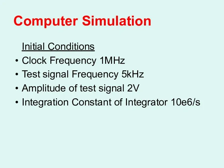
Computer Simulation
Initial Conditions
Clock Frequency 1MHz
Test signal Frequency 5kHz
Amplitude of test
Computer Simulation
Initial Conditions
Clock Frequency 1MHz
Test signal Frequency 5kHz
Amplitude of test
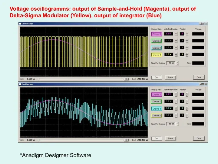
Voltage oscillogramms: output of Sample-and-Hold (Magenta), output of Delta-Sigma Modulator (Yellow),
Voltage oscillogramms: output of Sample-and-Hold (Magenta), output of Delta-Sigma Modulator (Yellow),
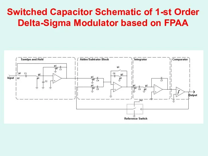
Switched Capacitor Schematic of 1-st Order Delta-Sigma Modulator based on FPAA
Switched Capacitor Schematic of 1-st Order Delta-Sigma Modulator based on FPAA
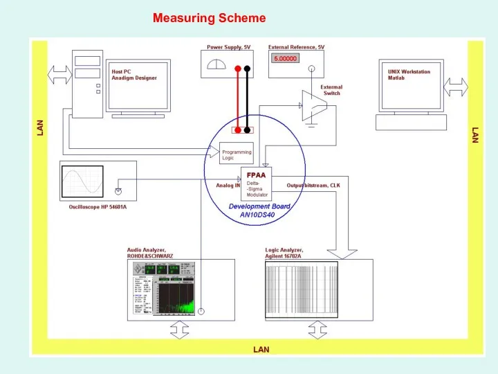
Measuring Scheme
Measuring Scheme
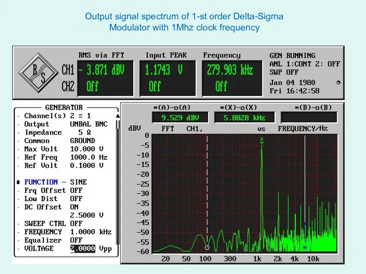
Output signal spectrum of 1-st order Delta-Sigma Modulator with 1Mhz clock
Output signal spectrum of 1-st order Delta-Sigma Modulator with 1Mhz clock
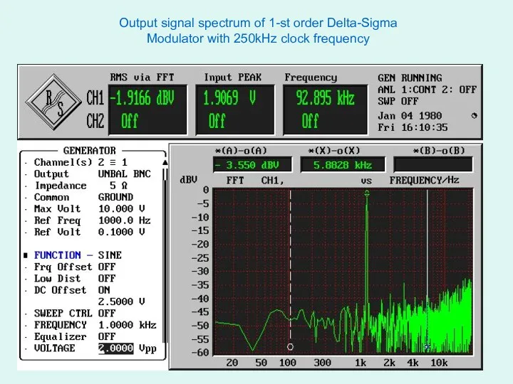
Output signal spectrum of 1-st order Delta-Sigma Modulator with 250kHz clock
Output signal spectrum of 1-st order Delta-Sigma Modulator with 250kHz clock
Conclusions
1.Proposed approaches are perspective and can be used for the CMOS
Conclusions
1.Proposed approaches are perspective and can be used for the CMOS
CONCLUSIONS
4. Simulation program has been proposed for analysis of oversampled switched-capacitor
CONCLUSIONS
4. Simulation program has been proposed for analysis of oversampled switched-capacitor
CONCLUSIONS
Delta-Sigma modulator has been realized on a basis of FPAA Anadigm
CONCLUSIONS
Delta-Sigma modulator has been realized on a basis of FPAA Anadigm
 Презентация к уроку физики в 7 классе Путешествие в Королевство Сил
 Использование ИКТ на уроках физики. Основная роль ИКТ в работе учителя
 Diffraction grating
 Жұмыс орындарындағы электромагниттік сәулеленулер
 Приборы электромагнитной и электродинамической систем
 Расчет давления жидкости на дно и стенки сосуда
 Определение по заданному обозначению посадки, предельных отклонений и размеров элементов деталей, допусков отверстия вала
 Основные понятия теории механизмов и машин
 Эксперимент – как метод активизации мыслительной деятельности учащихся на уроках физики
 Механизмдердің күштік талдауының кинеитостатикалық әдісі
 Оптика
 Методическая разработка урока Плотность вещества
 Кольца Ньютона
 Водородоподобные системы в квантовой механике
 Квалиметриялық шкалалар
 Презентация для 8 класса Испарение и конденсация
 Векторная диаграмма токов и напряжений
 Общая химическая технология. Кинетика ХТП. Понятия движущей силы. Лекция №1
 Ремонт и обслуживание проточного водонагревателя
 Гидравлический пресс
 Решение задач по геометрической оптике
 Механічна робота. Потужність
 Рентгенофазовый анализ
 Курс физики
 Презентация. Построение векторной диаграммы
 Презентация по физике для 10 класса МКТ газов
 Основные положения МКТ.
 Действие электрического тока на организм человека. (Лекция 6)