- Physical chemistry of nanostructured systems.( lecture no. 7)

Содержание
- 2. LECTURE No. 7 BASIC METHODS OF STUDYING NANOSTRUCTURED MATERIALS
- 3. INTRODUCTION The importance of the studying methods of nanostructured materials. Various techniques for detecting, measuring and
- 4. OBJECTIVES To describe how to characterize nanomaterials.
- 5. OUTLINE Electronic Microscopy Spectral methods of research Scanning Probe Test Methods
- 6. Electronic Microscopy Transmission Electron Microscope (TEM) Scanning Electron Microscope (SEM)
- 7. Electronic Microscopy Transmission Electron Microscope (TEM) Measures: particle size and characterization. Sample preparation: Sample preparation is
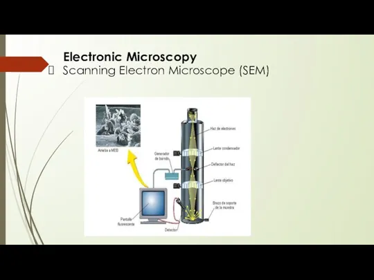
- 8. Electronic Microscopy Scanning Electron Microscope (SEM) Measures particle size and characterization. Sample: conductive or sputter coated.
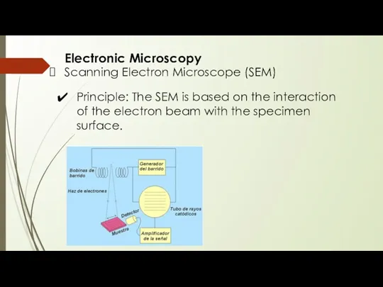
- 9. Electronic Microscopy Scanning Electron Microscope (SEM) Principle: The SEM is based on the interaction of the
- 10. Electronic Microscopy Scanning Electron Microscope (SEM)
- 11. Spectral methods of research Electronic Auger Spectroscopy (AES) Analytical technique used specifically in the study of
- 12. Spectral methods of research Secondary ion mass spectroscopy Analyze the composition of solid surfaces and thin
- 13. Spectral methods of research Laser microprobe analysis It uses a focused laser for microanalysis. It employs
- 14. Scanning Probe Test Methods The most widely used in the field of nanomaterials and nanotechnology. The
- 15. Scanning Probe Test Methods The cost and size of probe microscopes are usually much lower than
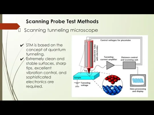
- 16. Scanning Probe Test Methods Scanning tunneling microscope STM is based on the concept of quantum tunneling.
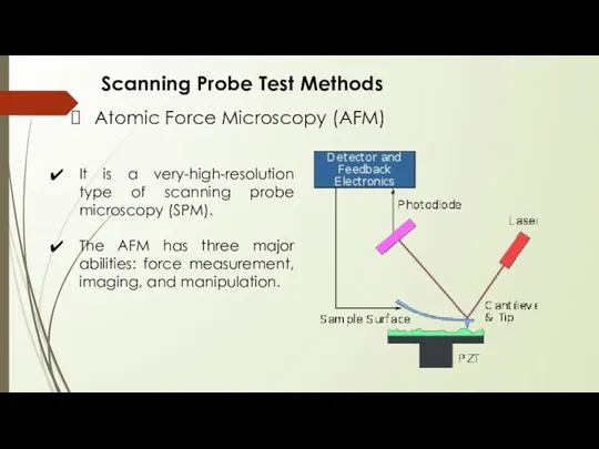
- 17. Scanning Probe Test Methods Atomic Force Microscopy (AFM) It is a very-high-resolution type of scanning probe
- 18. X-Ray Diffraction (XRD) Dynamic light scattering (DLS) Nanoparticle Surface Area Monitor (NSAM) Condensation Particle Counter (CPC)
- 19. Control questions What are the key parameters in the physical characterization of nanostructured materials? Describe the
- 21. Скачать презентацию
LECTURE No. 7
BASIC METHODS OF STUDYING NANOSTRUCTURED MATERIALS
LECTURE No. 7
BASIC METHODS OF STUDYING NANOSTRUCTURED MATERIALS
INTRODUCTION
The importance of the studying methods of nanostructured materials.
Various techniques for
INTRODUCTION
The importance of the studying methods of nanostructured materials.
Various techniques for
OBJECTIVES
To describe how to characterize nanomaterials.
OBJECTIVES
To describe how to characterize nanomaterials.
OUTLINE
Electronic Microscopy
Spectral methods of research
Scanning Probe Test Methods
OUTLINE
Electronic Microscopy
Spectral methods of research
Scanning Probe Test Methods
Electronic Microscopy
Transmission Electron Microscope (TEM)
Scanning Electron Microscope (SEM)
Electronic Microscopy
Transmission Electron Microscope (TEM)
Scanning Electron Microscope (SEM)
Electronic Microscopy
Transmission Electron Microscope (TEM)
Measures: particle size and characterization.
Sample preparation:
Electronic Microscopy
Transmission Electron Microscope (TEM)
Measures: particle size and characterization.
Sample preparation:
Electronic Microscopy
Scanning Electron Microscope (SEM)
Measures particle size and characterization.
Sample: conductive
Electronic Microscopy
Scanning Electron Microscope (SEM)
Measures particle size and characterization.
Sample: conductive
Electronic Microscopy
Scanning Electron Microscope (SEM)
Principle: The SEM is based on
Electronic Microscopy
Scanning Electron Microscope (SEM)
Principle: The SEM is based on
Electronic Microscopy
Scanning Electron Microscope (SEM)
Electronic Microscopy
Scanning Electron Microscope (SEM)
Spectral methods of research
Electronic Auger Spectroscopy (AES)
Analytical technique used specifically in
Spectral methods of research
Electronic Auger Spectroscopy (AES)
Analytical technique used specifically in
Spectral methods of research
Secondary ion mass spectroscopy
Analyze the composition of solid
Spectral methods of research
Secondary ion mass spectroscopy
Analyze the composition of solid
Spectral methods of research
Laser microprobe analysis
It uses a focused laser for
Spectral methods of research
Laser microprobe analysis
It uses a focused laser for
Scanning Probe Test Methods
The most widely used in the field of
Scanning Probe Test Methods
The most widely used in the field of
Scanning Probe Test Methods
The cost and size of probe microscopes are
Scanning Probe Test Methods
The cost and size of probe microscopes are
Scanning Probe Test Methods
Scanning tunneling microscope
STM is based on the
Scanning Probe Test Methods
Scanning tunneling microscope
STM is based on the
Scanning Probe Test Methods
Atomic Force Microscopy (AFM)
It is a very-high-resolution type
Scanning Probe Test Methods
Atomic Force Microscopy (AFM)
It is a very-high-resolution type
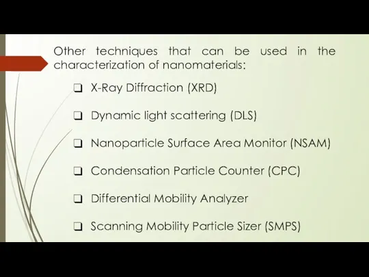
X-Ray Diffraction (XRD)
Dynamic light scattering (DLS)
Nanoparticle Surface Area Monitor (NSAM)
Dynamic light scattering (DLS)
Nanoparticle Surface Area Monitor (NSAM)
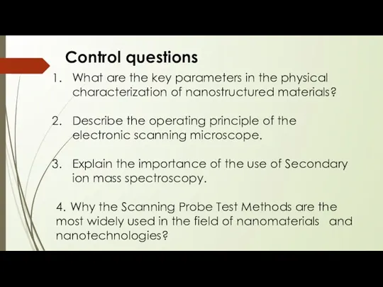
Control questions
What are the key parameters in the physical characterization of
Control questions
What are the key parameters in the physical characterization of
 Винтовые поверхности и изделия с резьбой. Крепежные изделия
 Зубчатые передачи
 Моменты импульса (угловые моменты). Часть вторая
 Градуировка спектроскопа
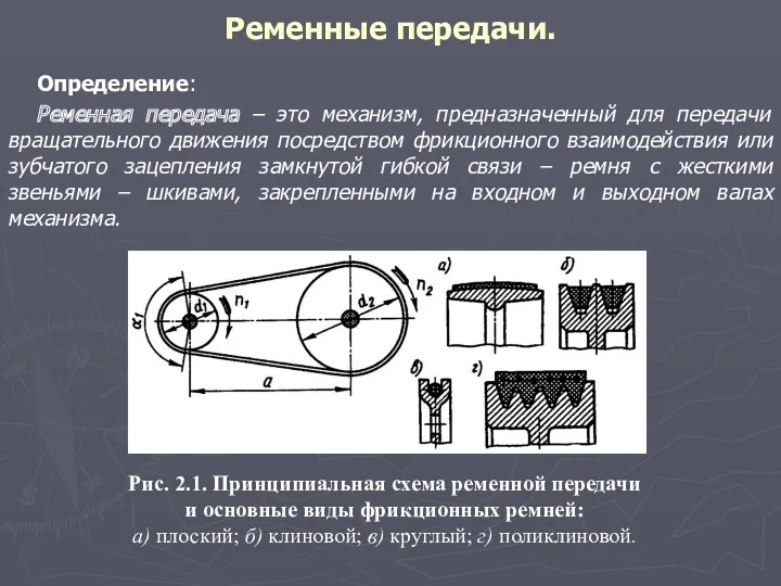 Ременные передачи
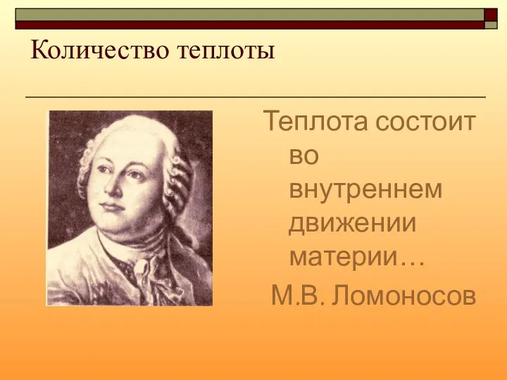 Количество теплоты
 Источники оптического импульсного когерентного излучения для информационных систем II. Полупроводниковые лазеры
 Разработка лаборатории по ремонту и диагностики топливных систем дизельных двигателей
 Техническое диагностирование автомобильной техники
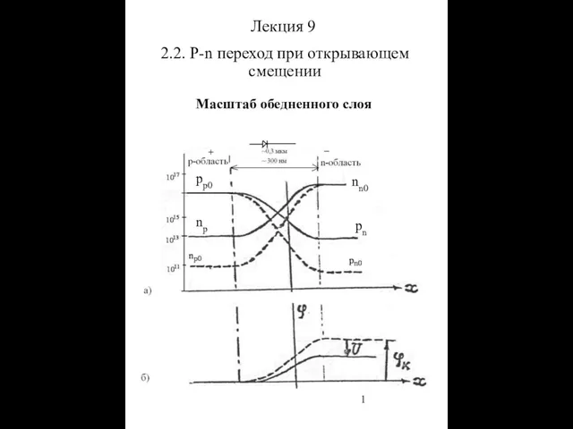 P-n переход при открывающем смещении. Масштаб обедненного слоя
 Тепломассообмен. Конвекция
 Кинематика материальной точки. Физические модели
 Основы физической реабилитации
 Физические и геологические основы сейсморазведки
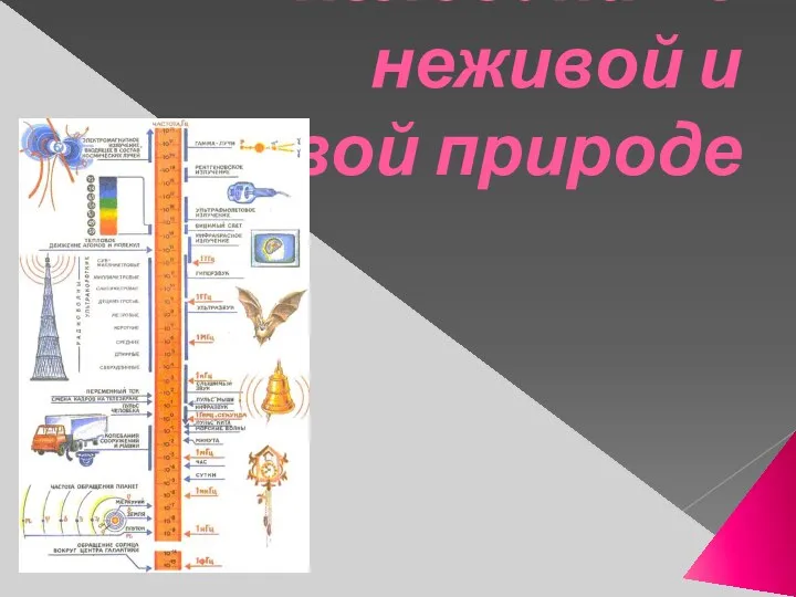 Колебания в неживой и живой природе. Урок 11
 Презентация. Законы Ньютона
 Презентация по теме Механические колебания
 Работа, кинетическая энергия
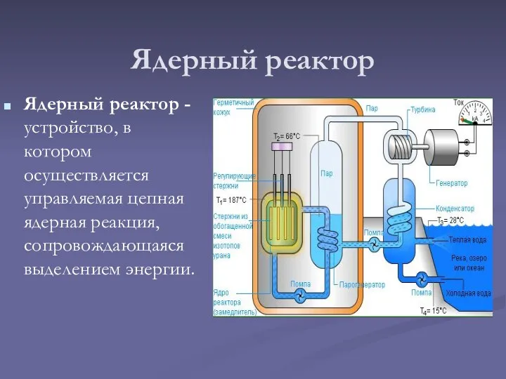 Ядерный реактор
 Проводниковые материалы
 Осесимметричные тонкостенные оболочки. Лекция 12
 Выяснение условия равновесия рычага
 Открытия М.В. Ломоносова в области физики и астрономии
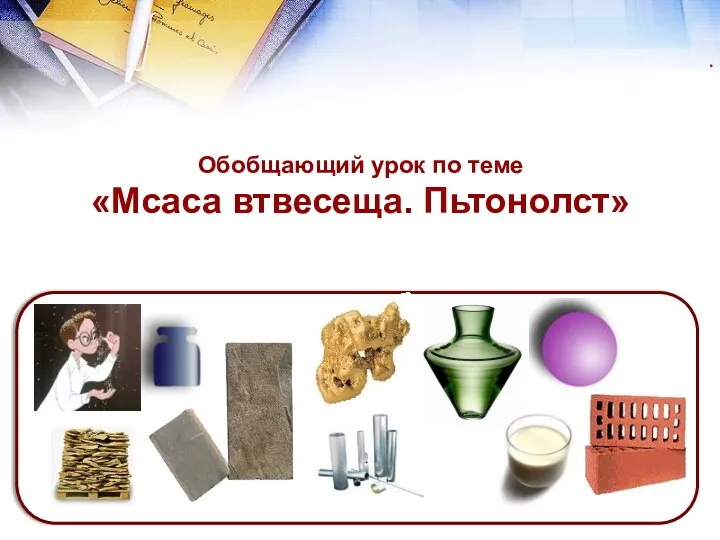 Масса вещества. Плотность
 Электрическая цепь и ее элементы
 Migrating from Streams to GoldenGate12c
 Электроразведка. Методы профилирования
 Управляемость автомобиля. Лекция № 11