- Surface plasma polaritons flow control using external fields

Содержание
- 2. Introduction Surface plasmon polaritons (SPPs) are generated as a result of the interaction of photons, phonons
- 3. Boundary conditions for the SPP for TM-mode SPP wavelength and propagation constant: – SPP wave vector
- 4. The real part of must be negative modulo should be greater than SPP excitation conditions -
- 5. Energy density flux distribution in a metal-insulator system The plasmon wave decays exponentially in the metal
- 6. (а) (б) Plasmofield effect transistor operating on the principle of a semiconductor n field effect transistor
- 7. A metal strip waveguide of length L, width 2a, thickness b, embedded in the dielectric. The
- 8. SPPs at the metal-insulator interface can exist only in the frequency region in which the dielectric
- 10. Скачать презентацию
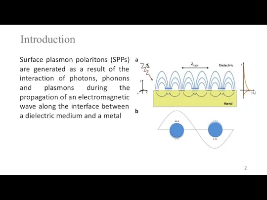
Introduction
Surface plasmon polaritons (SPPs) are generated as a result of the
Introduction
Surface plasmon polaritons (SPPs) are generated as a result of the
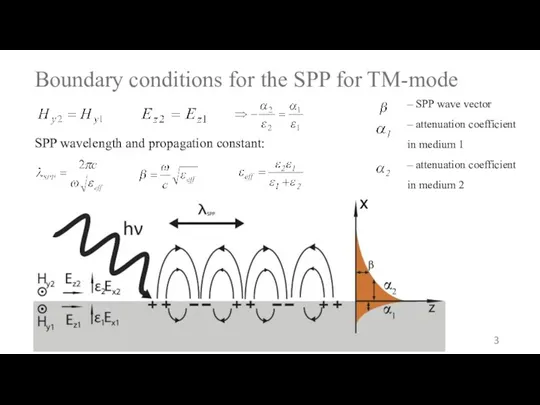
Boundary conditions for the SPP for TM-mode
SPP wavelength and propagation constant:
–
Boundary conditions for the SPP for TM-mode
SPP wavelength and propagation constant:
–
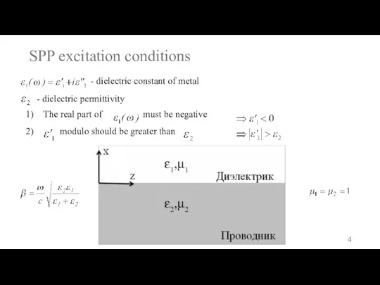
The real part of must be negative
modulo should be greater than
The real part of must be negative
modulo should be greater than
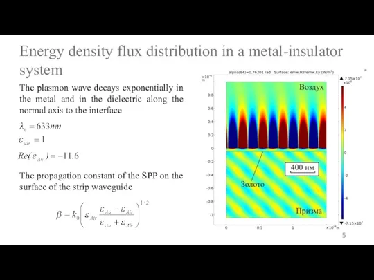
Energy density flux distribution in a metal-insulator system
The plasmon wave decays
Energy density flux distribution in a metal-insulator system
The plasmon wave decays
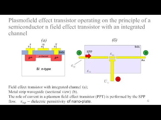
(а)
(б)
Plasmofield effect transistor operating on the principle of a semiconductor n
(а)
(б)
Plasmofield effect transistor operating on the principle of a semiconductor n
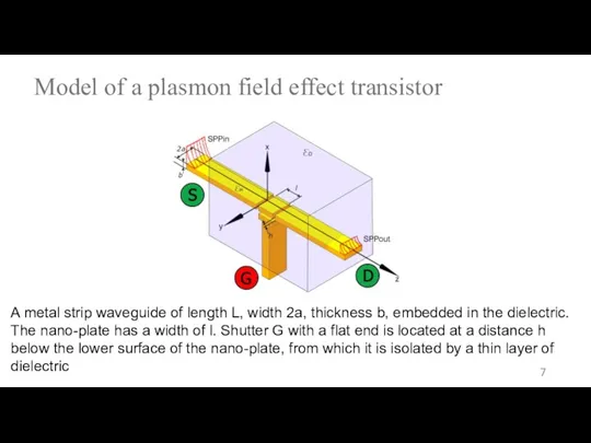
A metal strip waveguide of length L, width 2a, thickness b,
A metal strip waveguide of length L, width 2a, thickness b,
 Термодинамические циклы холодильных машин
 Замена радиатора в квартире
 Принцип работы тепловых машин
 Электродинамика. Электрический заряд
 Проводниковые материалы
 Плавление и отвердевание кристаллических тел. Удельная теплота плавления (урок 18)
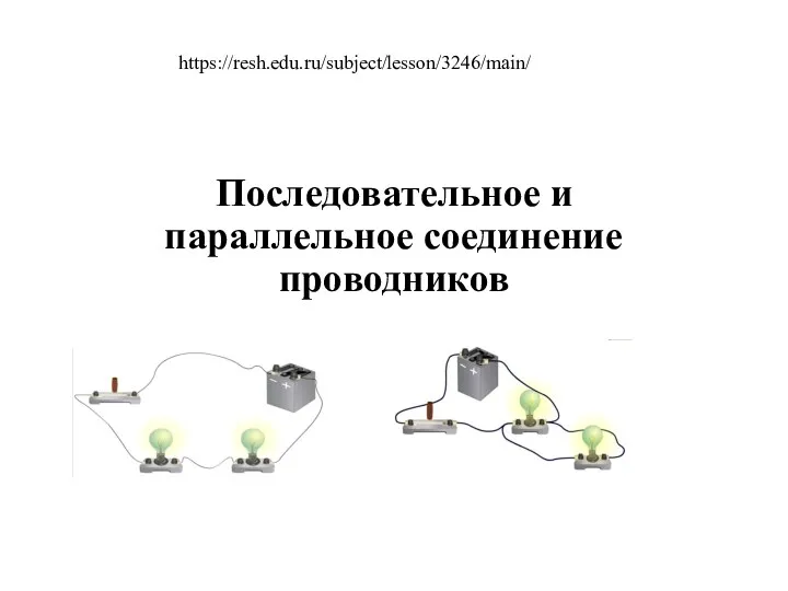 8Последовательное и параллельное соединение проводников
 Техническая термодинамика. Термодинамичекие потенциалы, эффект Джоуля-Томсона
 Основы теории напряженного состояния. Лекция 9
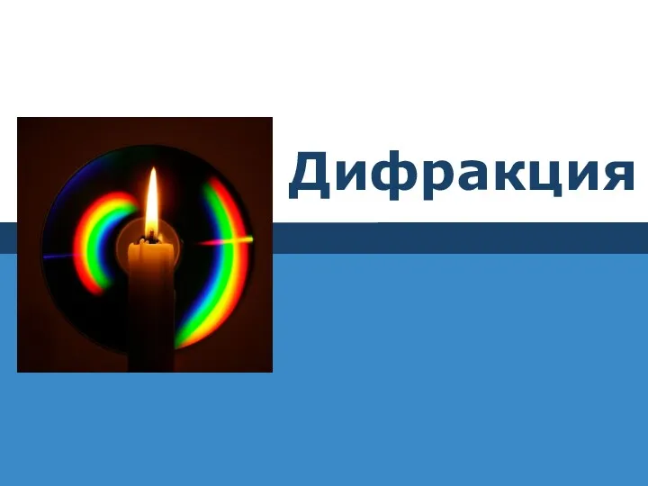 Дифракция.
 Земне тяжіння. Сила тяжіння. Вага тіла. Невагомість
 Насоси. Загальна характеристика насосів
 Урок мастерская Конвекция 8 класс первая часть
 Основні положення теорії надійності. (Лекція 6)
 Обобщающий урок в 8 классе по теме Электрические явления
 Теорема о движении центра масс
 Основное уравнение молекулярно-кинетической теории
 Уравнение состояния идеального газа. Газовые законы
 Электрохимические методы анализа. (Лекция 7)
 Формирование эксплуатационных характеристик энергоустановок современных транспортно-технологических машин
 teoriya_avtomaticheskogo_upravleniya_Polulah_parth4
 Резка металла
 Интегрированный урок физики и информатики
 Презентация к уроку Изменение агрегатных состояний вещества
 Реактивное движение. Ракеты. Урок физики в 9 классе
 Кинематика твердого тела введение
 Закон инерции Галилея – Ньютона. Принцип относительности Галилея. Преобразования Галилея
 Передача электромагнитной энергии. Волноводы