- Топологии импульсных преобразователей

Содержание
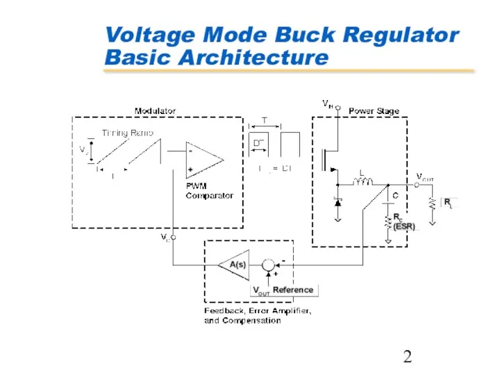
- 2. Voltage Mode Buck Regulator Basic Architecture
- 3. Feedback, Error Amplifier, and Compensation – Two Types Gm Amp: Op-Amp: Gain is a function of
- 4. Modulator and Power Stage gain: Feedback, Error Amplifier, and Compensation gain (Gm-type Error Amp): Regulator loop
- 5. Voltage-Mode Buck Regulator Frequency Response Gain (dB) freq (Hz) φ (deg) 0 0 φM f0 -40dB/dec
- 6. Current Mode Buck Regulator Basic Architecture
- 7. Gain of Modulator and Power Stage: Se = corrective ramp slope Sn = positive slope current-sense
- 8. Current Mode Buck Regulator Loop Gain Feedback, Error Amplifier, and Compensation gain (Gm-type Error Amp): Regulator
- 9. Current-Mode Buck Regulator Frequency Response Gain (dB) freq (Hz) φ (deg) 0 0 φM f0 -20dB/dec
- 10. Hysteretic Buck Regulator Basic Architecture
- 11. Hysteretic Buck Regulator Switching Waveforms tON and tOFF are functions of VIN, VOUT, L, ESR, ESL,
- 12. In most cases, switching frequency is determined by output ripple voltage (ΔVOUT) resulting from ESR. Amplitude
- 13. Compensating for excessive ESL in output capacitor COUT has excessive ESL, so ΔVOUT has large voltage
- 14. Constant On-Time Buck Regulator Basic Architecture
- 15. Constant On-time Buck Regulator Switching Waveforms tON is set by a one-shot timer that decreases tON
- 17. Скачать презентацию
Voltage Mode Buck Regulator
Basic Architecture
Voltage Mode Buck Regulator
Basic Architecture
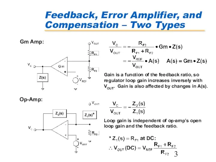
Feedback, Error Amplifier, and Compensation – Two Types
Gm Amp:
Op-Amp:
Gain is a
Feedback, Error Amplifier, and Compensation – Two Types
Gm Amp:
Op-Amp:
Gain is a
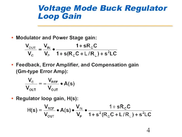
Modulator and Power Stage gain:
Feedback, Error Amplifier, and Compensation gain
(Gm-type Error
Modulator and Power Stage gain:
Feedback, Error Amplifier, and Compensation gain
(Gm-type Error
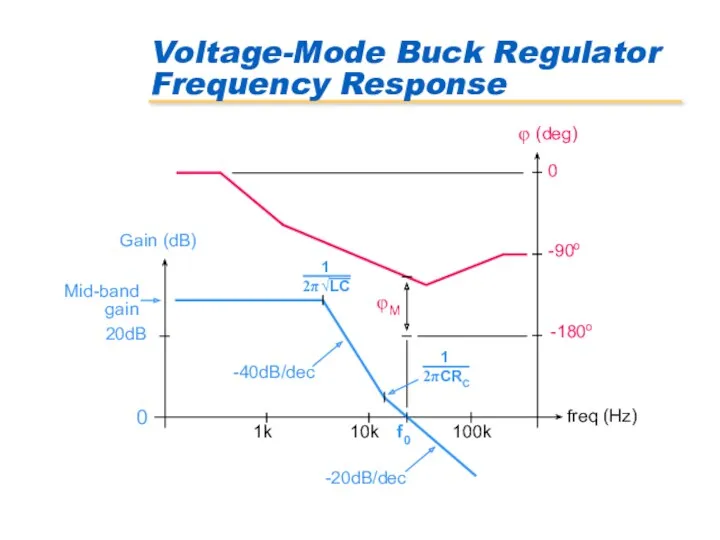
Voltage-Mode Buck Regulator
Frequency Response
Gain (dB)
freq (Hz)
φ (deg)
0
0
φM
f0
-40dB/dec
-20dB/dec
-90o
-180o
20dB
1k
10k
100k
Mid-band gain
Voltage-Mode Buck Regulator
Frequency Response
Gain (dB)
freq (Hz)
φ (deg)
0
0
φM
f0
-40dB/dec
-20dB/dec
-90o
-180o
20dB
1k
10k
100k
Mid-band gain
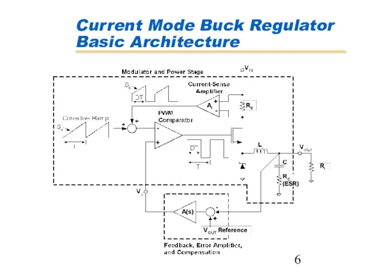
Current Mode Buck Regulator Basic Architecture
Current Mode Buck Regulator Basic Architecture
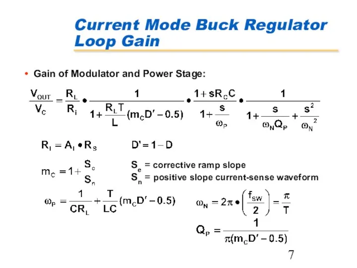
Gain of Modulator and Power Stage:
Se = corrective ramp slope
Sn =
Gain of Modulator and Power Stage:
Se = corrective ramp slope
Sn =
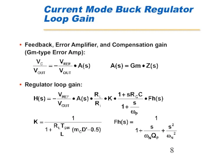
Current Mode Buck Regulator
Loop Gain
Feedback, Error Amplifier, and Compensation gain
(Gm-type Error
Current Mode Buck Regulator
Loop Gain
Feedback, Error Amplifier, and Compensation gain
(Gm-type Error
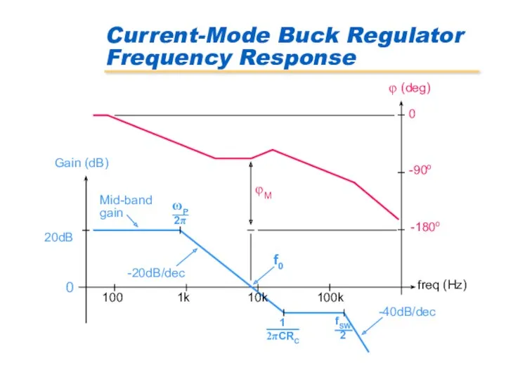
Current-Mode Buck Regulator
Frequency Response
Gain (dB)
freq (Hz)
φ (deg)
0
0
φM
f0
-20dB/dec
-90o
-180o
20dB
1k
10k
100k
Mid-band gain
100
fSW
2
-40dB/dec
Current-Mode Buck Regulator
Frequency Response
Gain (dB)
freq (Hz)
φ (deg)
0
0
φM
f0
-20dB/dec
-90o
-180o
20dB
1k
10k
100k
Mid-band gain
100
fSW
2
-40dB/dec
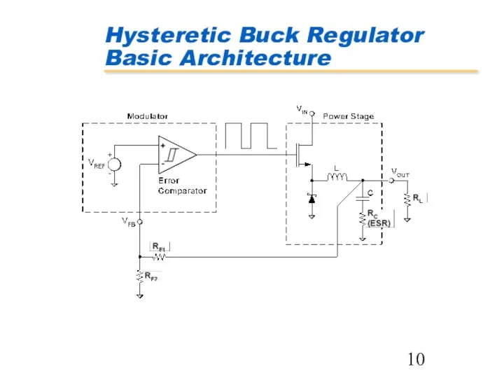
Hysteretic Buck Regulator Basic Architecture
Hysteretic Buck Regulator Basic Architecture
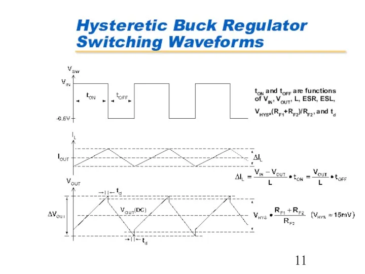
Hysteretic Buck Regulator Switching Waveforms
tON and tOFF are functions of VIN,
Hysteretic Buck Regulator Switching Waveforms
tON and tOFF are functions of VIN,
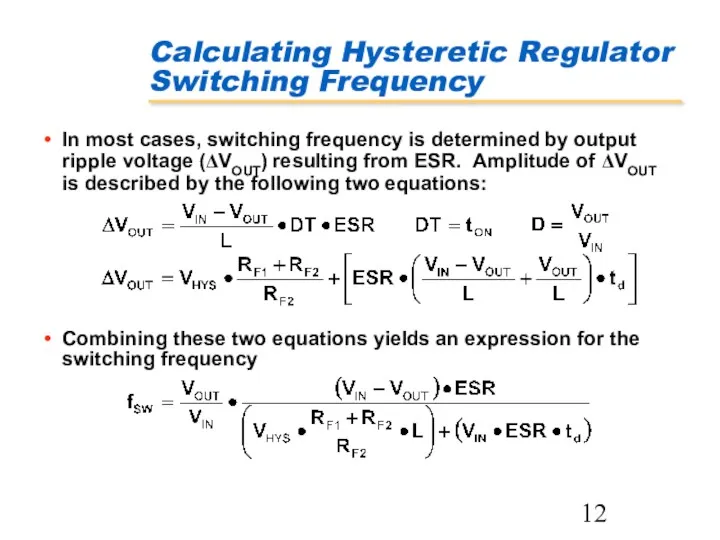
In most cases, switching frequency is determined by output ripple voltage
In most cases, switching frequency is determined by output ripple voltage
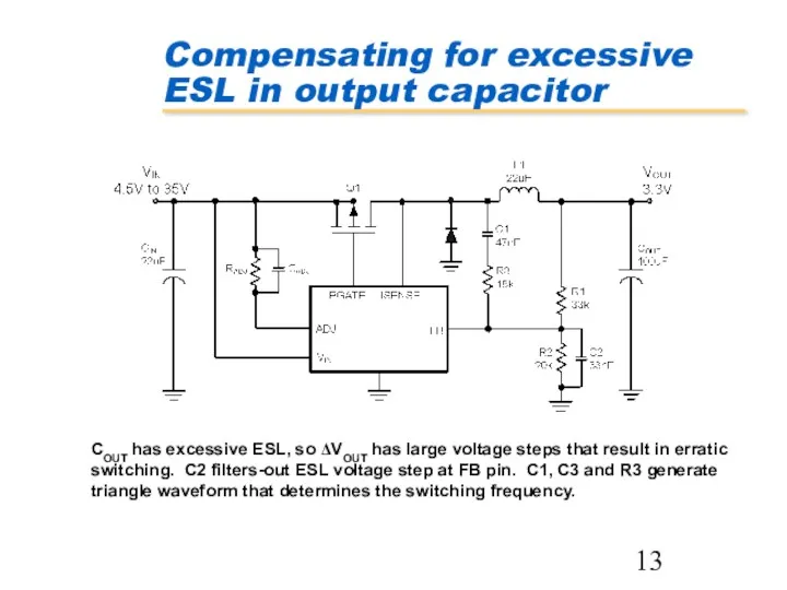
Compensating for excessive ESL in output capacitor
COUT has excessive ESL, so
Compensating for excessive ESL in output capacitor
COUT has excessive ESL, so
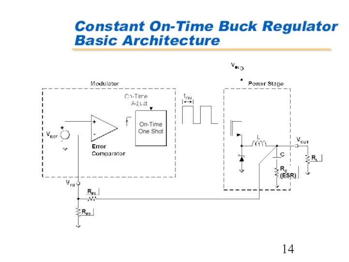
Constant On-Time Buck Regulator Basic Architecture
Constant On-Time Buck Regulator Basic Architecture
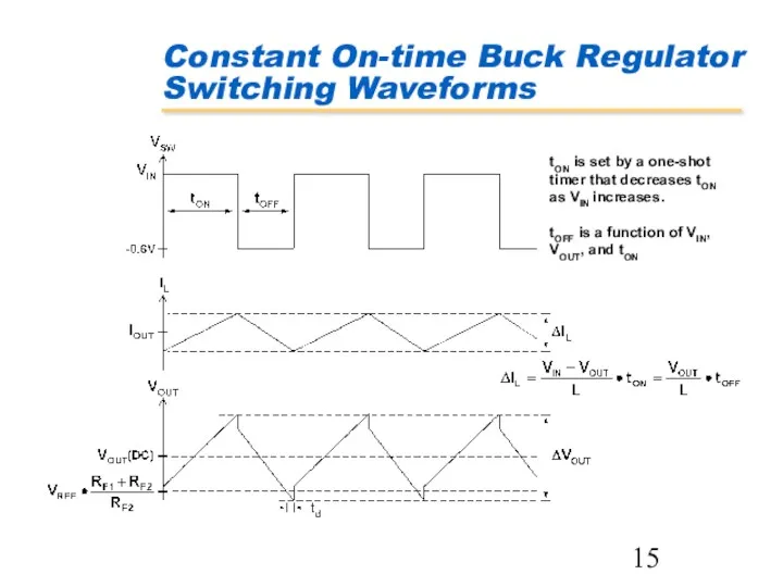
Constant On-time Buck Regulator Switching Waveforms
tON is set by a one-shot
Constant On-time Buck Regulator Switching Waveforms
tON is set by a one-shot
 Кривошипно- шатунный механизм
 Исследование колебаний маятников различных видов
 История радиосвязи
 презентация Чудеса света
 Электромагнитная индукция
 Презентация Дорога человечества в космос
 Открытый урок по теме Молекулярная физика
 Определение предмета биофизики
 Сила трения. Трение в природе и технике
 Защита от грозовых и коммутационных перенапряжений
 Магнит өрісіндегі тогы бар контур
 Магнитное поле и его графическое изображение
 Биохимический анализ. Фотометрия. Основные принципы
 Физика. Разделы физики
 урок по теме плотность вещества
 Техническое обслуживание и ремонт систем энергообеспечения и запуска двигателя
 Антенні та фідерні пристрої ЗРЛ. Загальні відомості і принцип дії фідерних пристроїв. (Тема 3.1)
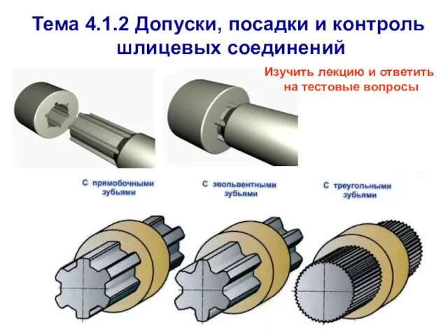 Допуски, посадки и контроль шлицевых соединений деталей
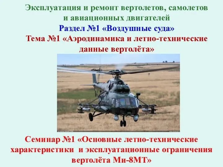 Аэродинамика и летно-технические данные вертолёта. Тема №1. Основные летно-технические характеристики. Семинар №1
 Общие сведения о направляющих системах
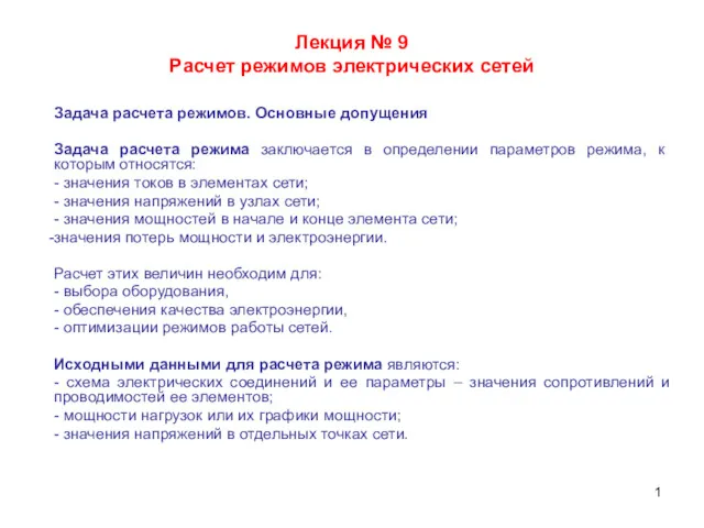 Расчет режимов электрических сетей
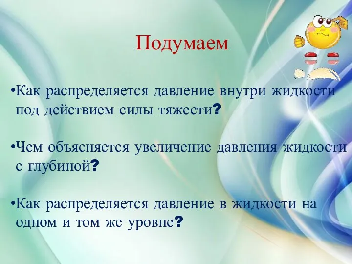 Действие жидкости и газа на погруженное в них тело
 Элементарные частицы
 Техническое обслуживание и ремонт тормозной системы трактора
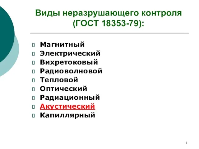 Раздел 1. Акустические преобразователи. Классификация
 Теплоотдача при поперечном обтекании труб
 Режущий инструмент. Основные функции. Основы теории режущих инструментов
 Эксергия. Термодинамические процессы в газах, парах и их смесях. (Занятие 4)