- Computer Architecture WS 2005-2006

Содержание
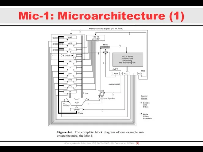
- 2. Mic-1: Microarchitecture (1) ()
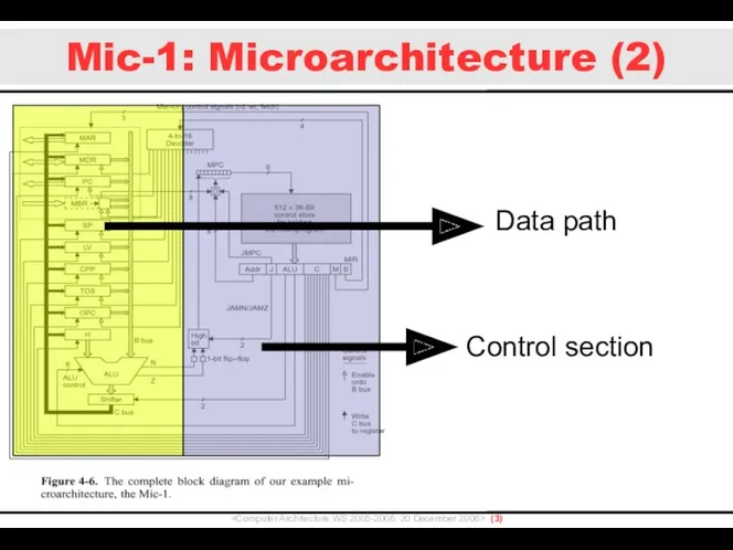
- 3. Mic-1: Microarchitecture (2) () Data path Control section
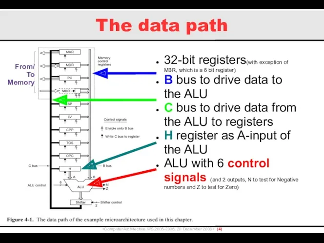
- 4. The data path () 32-bit registers(with exception of MBR, which is a 8 bit register) B
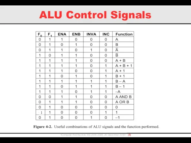
- 5. ALU Control Signals () 1
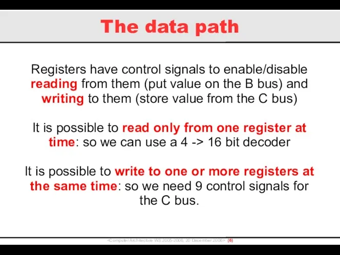
- 6. The data path () Registers have control signals to enable/disable reading from them (put value on
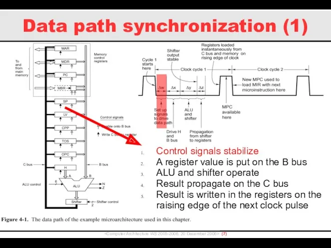
- 7. Data path synchronization (1) () Control signals stabilize A register value is put on the B
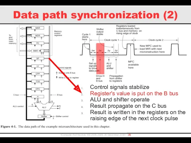
- 8. Data path synchronization (2) () Control signals stabilize Register's value is put on the B bus
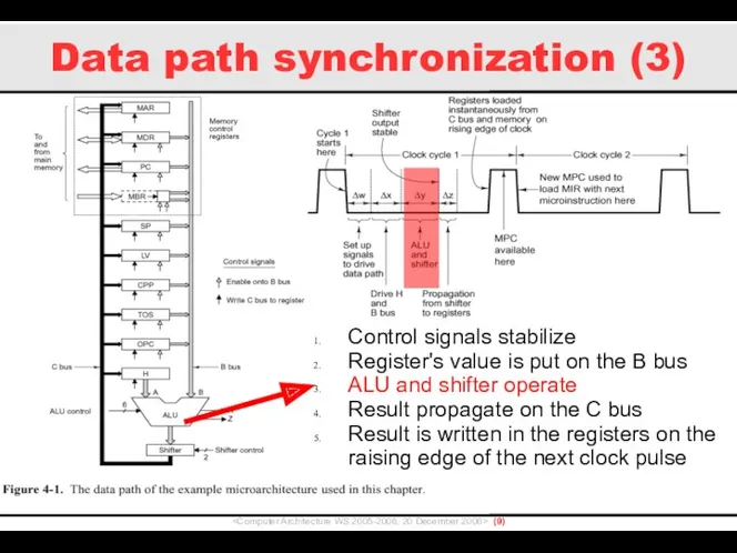
- 9. Data path synchronization (3) () Control signals stabilize Register's value is put on the B bus
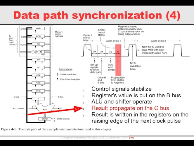
- 10. Data path synchronization (4) () Control signals stabilize Register's value is put on the B bus
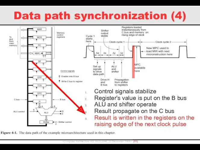
- 11. Data path synchronization (4) () Control signals stabilize Register's value is put on the B bus
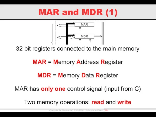
- 12. MAR and MDR (1) () 32 bit registers connected to the main memory MAR = Memory
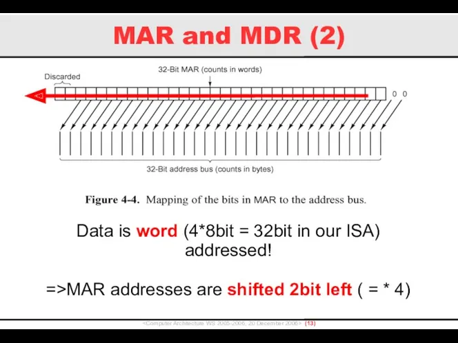
- 13. MAR and MDR (2) () Data is word (4*8bit = 32bit in our ISA) addressed! =>MAR
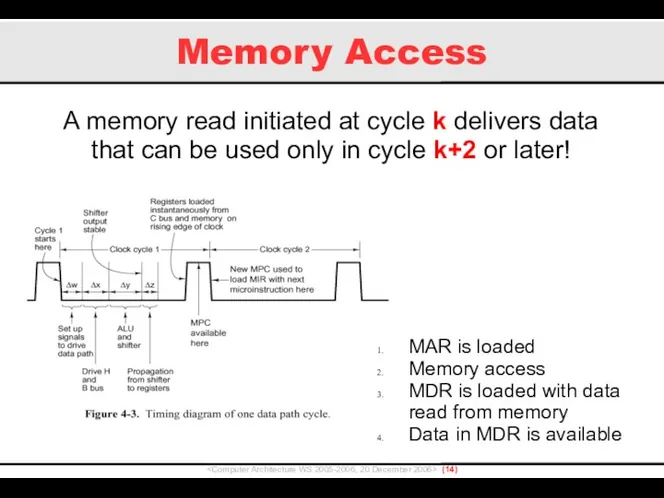
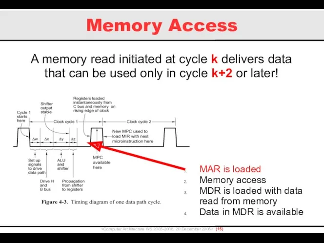
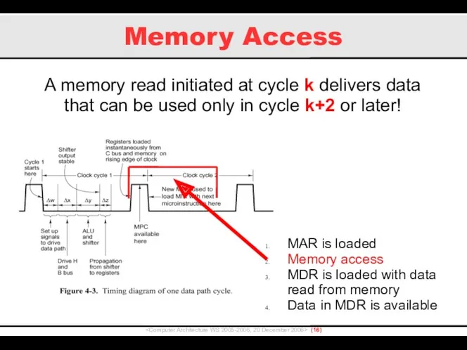
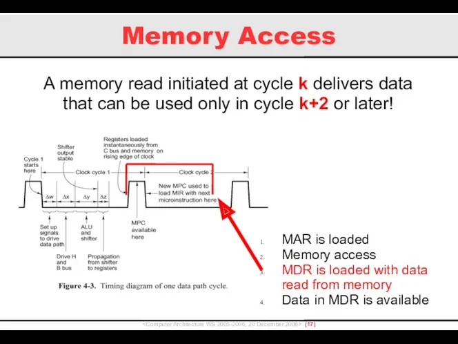
- 14. Memory Access () A memory read initiated at cycle k delivers data that can be used
- 15. Memory Access () A memory read initiated at cycle k delivers data that can be used
- 16. Memory Access () A memory read initiated at cycle k delivers data that can be used
- 17. Memory Access () A memory read initiated at cycle k delivers data that can be used
- 18. Memory Access () A memory read initiated at cycle k delivers data that can be used
- 19. Memory Access (2) () Until start of cycle k+2 the MDR register contains old data It
- 20. PC and MBR () 8 bit registers connected to the main memory used to read (fetch)
- 21. H register () Is the A-input of the ALU Has only one control signal; output to
- 22. ISA, IJVM, Microarchitecture () ISA = Instruction Set Architecture (defines instructions, memory model, available registers,...) IJVM
- 23. Mic-1 implementation () The Mic-1 is a microprogrammed architecture: each IJVM instruction (Macroinstruction) is divided one
- 24. Control section () MicroProgram Counter (MPC) Control store holding microinstructions MicroInstruction Register (MIR) containing current microinstruction
- 25. Microinstructions () 36bit wide microinstructions Microinstructions are “executed” in the control section (“a CPU in the
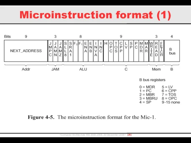
- 26. Microinstruction format (1) ()
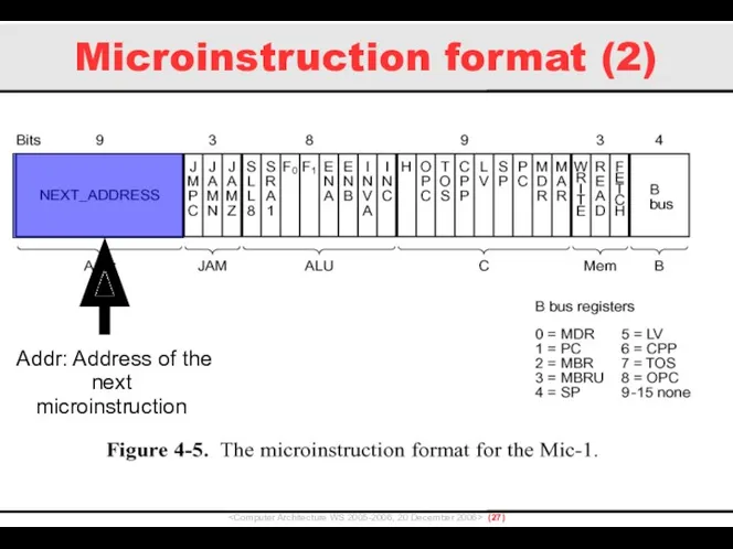
- 27. Microinstruction format (2) () Addr: Address of the next microinstruction
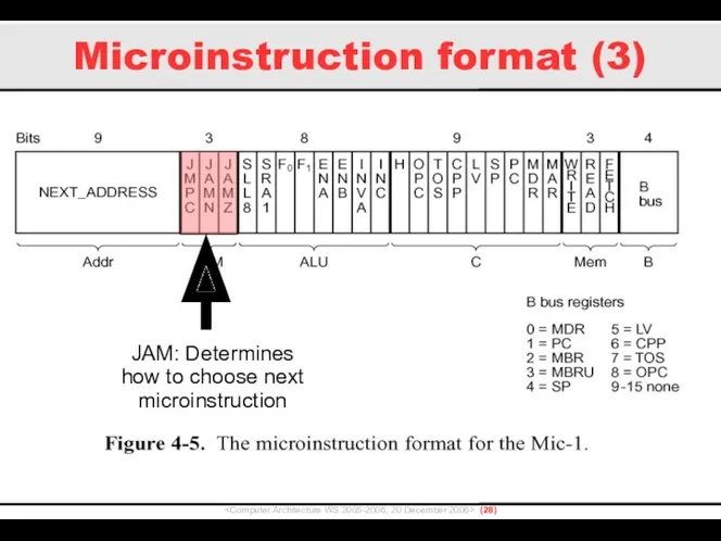
- 28. Microinstruction format (3) () JAM: Determines how to choose next microinstruction
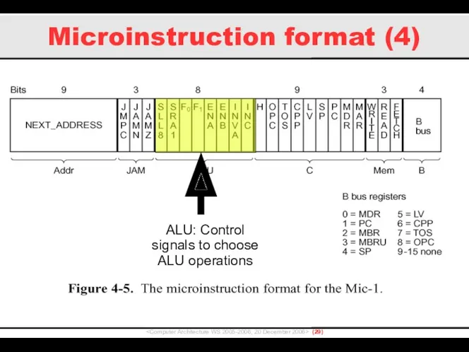
- 29. Microinstruction format (4) () ALU: Control signals to choose ALU operations
- 30. Microinstruction format (5) () C: Enables writing from C bus to the selected registers
- 31. Microinstruction format (6) () Mem: Controls memory read/write/fetch operations
- 32. Microinstruction format (7) () B: Controls which register can write to the B bus
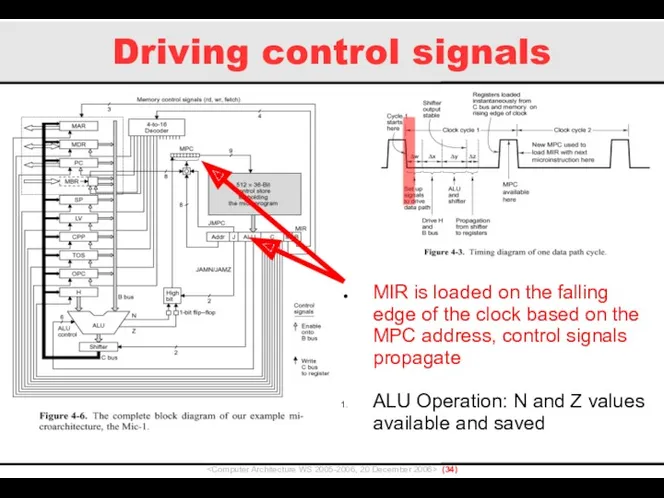
- 33. Driving control signals () MIR is loaded on the falling edge of the clock based on
- 34. Driving control signals () MIR is loaded on the falling edge of the clock based on
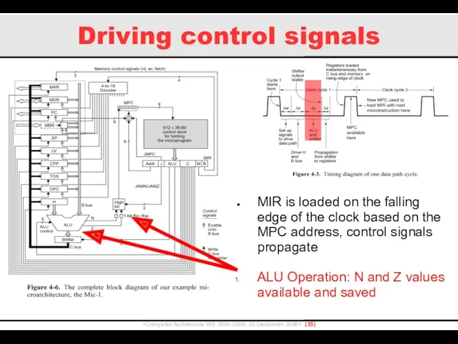
- 35. Driving control signals () MIR is loaded on the falling edge of the clock based on
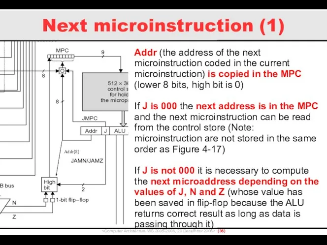
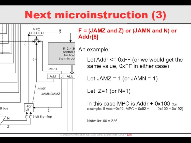
- 36. Next microinstruction (1) () Addr (the address of the next microinstruction coded in the current microinstruction)
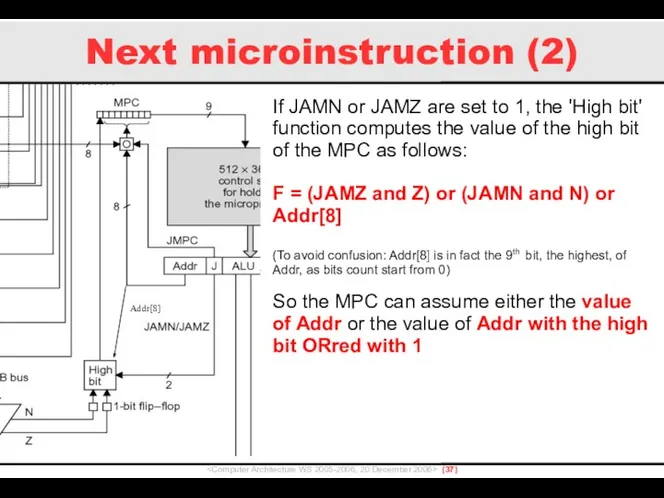
- 37. Next microinstruction (2) () If JAMN or JAMZ are set to 1, the 'High bit' function
- 38. Next microinstruction (3) () F = (JAMZ and Z) or (JAMN and N) or Addr[8] An
- 39. Microinstructions (4) () ...but why is all that stuff required to determine the next microinstruction ?
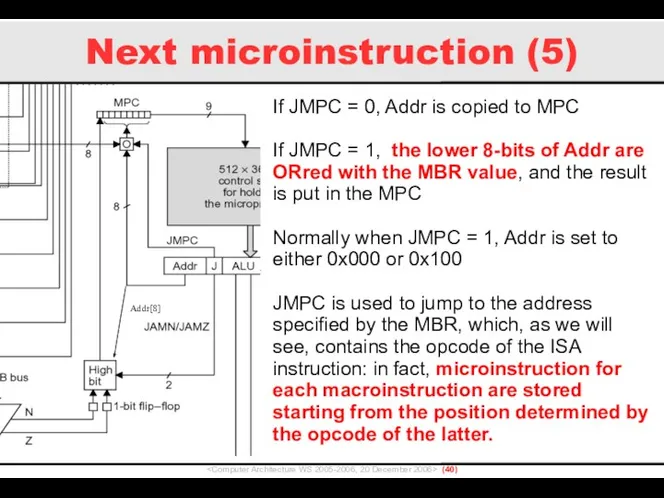
- 40. Next microinstruction (5) () If JMPC = 0, Addr is copied to MPC If JMPC =
- 42. Скачать презентацию
Mic-1: Microarchitecture (1)
()
Mic-1: Microarchitecture (1)
Mic-1: Microarchitecture (2)
()
Data path
Control
Mic-1: Microarchitecture (2)
Data path
Control
The data path
()
32-bit registers(with
The data path
32-bit registers(with
ALU Control Signals
()
1
ALU Control Signals
1
The data path
()
Registers have
The data path
Registers have
Data path synchronization (1)
()
Control
Data path synchronization (1)
Control
Data path synchronization (2)
()
Control
Data path synchronization (2)
Control
Data path synchronization (3)
()
Control
Data path synchronization (3)
Control
Data path synchronization (4)
()
Control
Data path synchronization (4)
Control
Data path synchronization (4)
()
Control
Data path synchronization (4)
Control
MAR and MDR (1)
()
32
MAR and MDR (1)
32
MAR and MDR (2)
()
Data
MAR and MDR (2)
Data
Memory Access
()
A memory read
Memory Access
A memory read
Memory Access
()
A memory read
Memory Access
A memory read
Memory Access
()
A memory read
Memory Access
A memory read
Memory Access
()
A memory read
Memory Access
A memory read
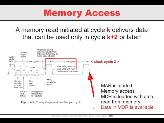
Memory Access
()
A memory read
Memory Access
A memory read
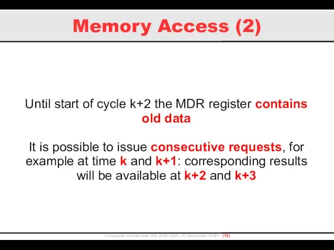
Memory Access (2)
()
Until start
Memory Access (2)
Until start
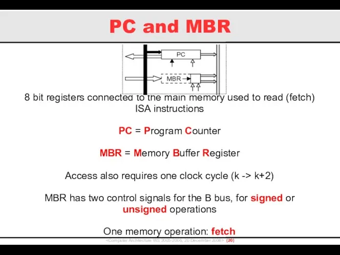
PC and MBR
()
8 bit
PC and MBR
8 bit
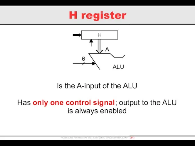
H register
()
Is the A-input
H register
Is the A-input
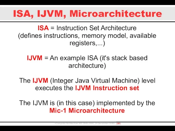
ISA, IJVM, Microarchitecture
()
ISA =
ISA, IJVM, Microarchitecture
ISA =
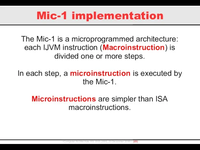
Mic-1 implementation
()
The Mic-1 is
Mic-1 implementation
The Mic-1 is
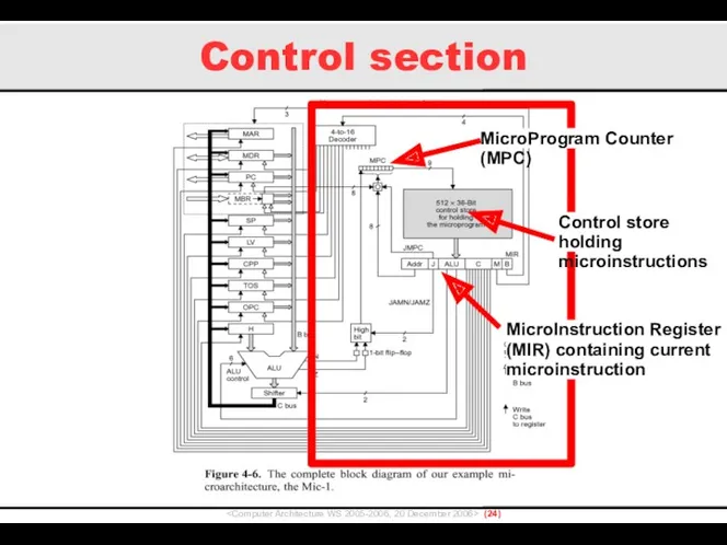
Control section
()
MicroProgram Counter
Control section
MicroProgram Counter
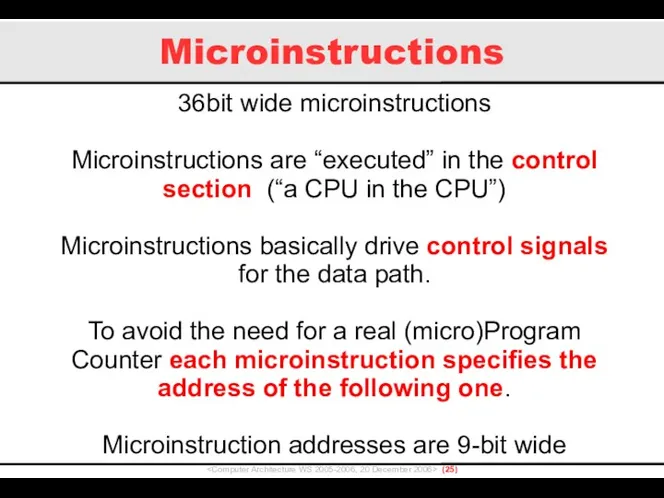
Microinstructions
()
36bit wide microinstructions
Microinstructions are
Microinstructions
36bit wide microinstructions
Microinstructions are
Microinstruction format (1)
()
Microinstruction format (1)
Microinstruction format (2)
()
Addr:
Microinstruction format (2)
Addr:
Microinstruction format (3)
()
JAM:
Microinstruction format (3)
JAM:
Microinstruction format (4)
()
ALU:
Microinstruction format (4)
ALU:
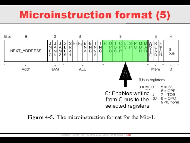
Microinstruction format (5)
()
C:
Microinstruction format (5)
C:
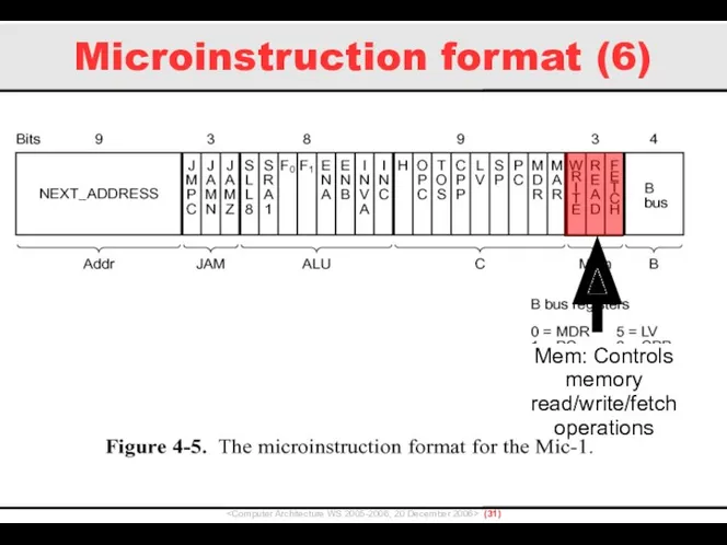
Microinstruction format (6)
()
Mem:
Microinstruction format (6)
Mem:
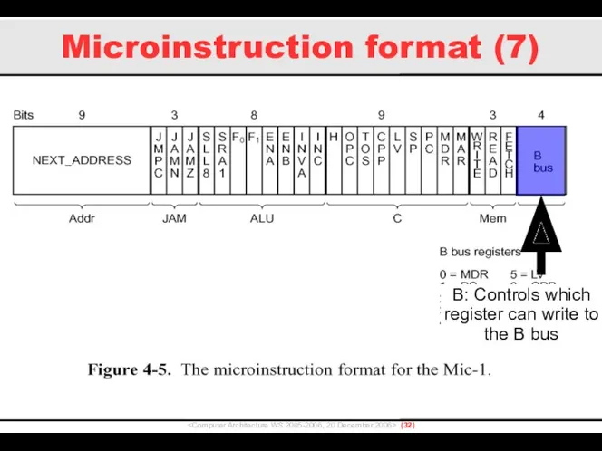
Microinstruction format (7)
()
B:
Microinstruction format (7)
B:
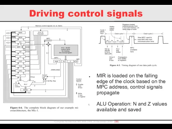
Driving control signals
()
MIR is
Driving control signals
MIR is
Driving control signals
()
MIR is
Driving control signals
MIR is
Driving control signals
()
MIR is
Driving control signals
MIR is
Next microinstruction (1)
()
Addr (the
Next microinstruction (1)
Addr (the
Next microinstruction (2)
()
If JAMN
Next microinstruction (2)
If JAMN
Next microinstruction (3)
()
F =
Next microinstruction (3)
F =
Microinstructions (4)
()
...but why is
Microinstructions (4)
...but why is
Next microinstruction (5)
()
If JMPC
Next microinstruction (5)
If JMPC
 Алгоритмы и исполнители. (5 класс)
 Настройка маршрутизаторов DIR-300 и DIR-400 для работы в сети провайдера SKYNET* при помощи авторизатора
 Элементы теории алгоритмов
 Растровая и векторная графика
 Актуалізація опорних знань. (інформатика 7 класс)
 Как сделать сайт максимально эффективным?
 Программирование на стороне сервера. PHP
 Алгоритмдеу жєне программалау
 Алгоритмы STL
 Газета совета студенческого самоуправления
 Компьютерные курсы. Создание трехмерных игр на движке Unity Юниум
 Показатели публикационной активности как критерий оценки конкурентоспособности
 Алгоритмы со структурой Выбор. Урок 31
 Communicating WNCRY
 История развития систем защиты информации
 Hibernate query language (HQL)
 iSpring Suite 8. Быстрый инструмент для создания электронных курсов и тестов в PowerPoint
 Как появился компьютер, информатика 3 класс
 Поиск информации в сети Internet
 Презентация к уроку информатики 3класс по теме Ориентированный граф
 Информационные ресурсы
 Услуга Мобильные Сотрудники. МТС
 Основы сетей передачи данных. Общие принципы построения сетей. Коммутация каналов и пакетов
 Использование компьютерных технологий в детском саду.
 fbea8-fe014e85
 Текстовий редактор Word
 Технология Умный дом
 Скрипты Перезвон, Обзвон по базе