- Advanced Configuration and Power Interface

Содержание
- 2. OUTLINE Advanced Configuration and Power Interface Before Power On Voltage and Signal Power Supply and Stand
- 3. Advanced Configuration and Power Interface
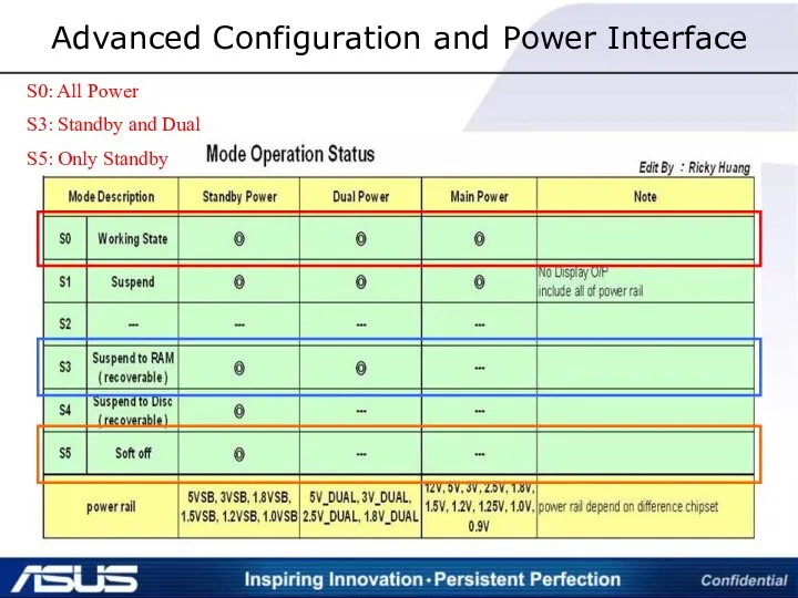
- 4. Advanced Configuration and Power Interface S0: All Power S3: Standby and Dual S5: Only Standby
- 5. Before Power On Voltage and Signal
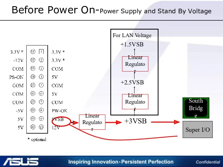
- 6. Before Power On-Power Supply and Stand By Voltage
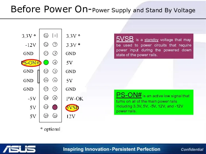
- 7. Before Power On-Power Supply and Stand By Voltage PS-ON# is an active low signal that turns
- 8. Before Power On-Power Supply and Stand By Voltage
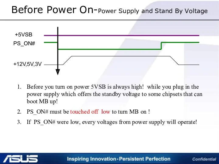
- 9. Before Power On-Power Supply and Stand By Voltage Before you turn on power 5VSB is always
- 10. Before Power On-PWRBTN#, RSTCON#, RSMRST#,PS_ON# +3VSB GND +5VSB +3VSB 1. 2. 3. 3. Super I/O Power
- 11. Before Power On-PWRBTN#, RSTCON#, RSMRST#,PS_ON# +3VSB GND +5VSB +3VSB 1. 2. 3. 3. Super I/O RSTCON#
- 12. Before Power On-PWRBTN#, RSTCON#, RSMRST#,PS_ON# When 5VSB and 3VSB send to SIO and SB SIO will
- 13. Before Power On-PWRBTN#, RSTCON#, RSMRST#,PS_ON# Power Button#
- 14. Before Power On-Battery Voltage Function of Battery Power are: CMOS SRAM Real Time Clock
- 15. Before Power On-Battery Voltage Before boot up the board, please check the jumper in normal status.
- 16. Before Power On-Battery Voltage South Bridge + 3VSB Battery RTCRST# 32.7 KHz CLR CMOS 1kohm *Current
- 17. Before Power On-Battery Voltage Use Multi-meter to measure Current Leakage value START Check Vbatt related Components
- 18. Before Power On-Battery Voltage 1 1. Use multi-meter to measure 1k ohm near the battery circuit,
- 19. Before Power On-Battery Voltage 3 3. If the value is still NG, check the diode (RB715F)
- 20. AFTER POWER ON VOLTAGE
- 21. After Power On-Voltage Distribution
- 22. After Power On-Voltage Distribution M4A79T DELUXE
- 23. After Power On-Linear & Switch Regulator introduction 1. Linear Regulator – Lower Cost and Higher heat.
- 24. After Power On-Linear & Switch Regulator introduction MOSFET N channel, Current high If G is hi,
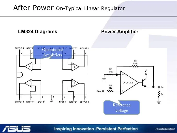
- 25. After Power On-Typical Linear Regulator
- 26. After Power On-Typical Linear Regulator LM324 Diagrams Power Amplifier Operational Amplifiers Reference voltage
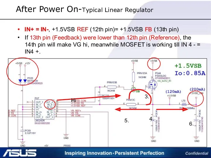
- 27. IN+ = IN-, +1.5VSB REF (12th pin)= +1.5VSB FB (13th pin) If 13th pin (Feedback) were
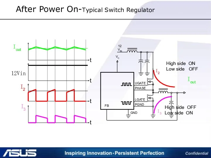
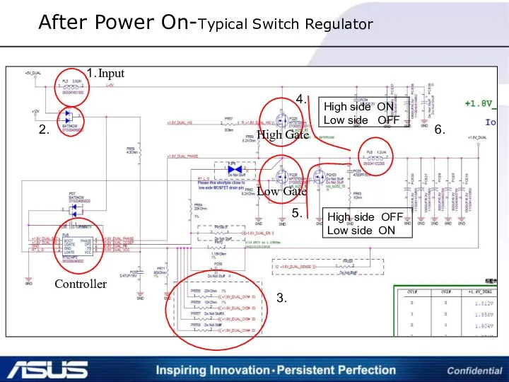
- 28. After Power On-Typical Switch Regulator
- 29. After Power On-Typical Switch Regulator
- 30. After Power On-Typical Switch Regulator
- 31. VCORE
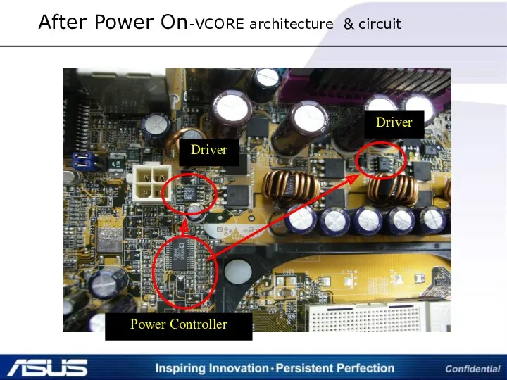
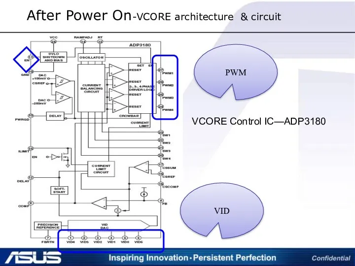
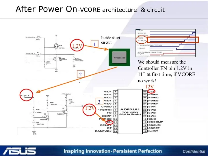
- 32. After Power On-VCORE architecture & circuit
- 33. VID PWM VCORE After Power On-VCORE architecture & circuit
- 34. After Power On-VCORE architecture & circuit PWM
- 35. VID PWM VCORE Control IC—ADP3180 After Power On-VCORE architecture & circuit
- 36. After Power On-VCORE architecture & circuit
- 37. CPU VID4 VID3 VID2 VID1 VID0 +5V 1K 10K Switching Regulator Vcore 0 (Low Level) :0V
- 38. ADP3180 Output Voltage V.S. VID code After Power On-VCORE architecture & circuit
- 39. After Power On-VCORE Voltage repair Flow Chart 1
- 40. Turn off Power Supply Remove Power Supply cable NO Remove all abnormal MOS which DGS is
- 41. Mount good MOS and Driver Other root cause like soldering short. NO Other rootcause like Socket
- 42. After Power On-VCORE Problem Debug Procedure (1) If no Output Check if both 5V and 12V
- 43. If the output voltage wrong Check if VIDs of Power Regulator are wrong setting Check if
- 45. Скачать презентацию
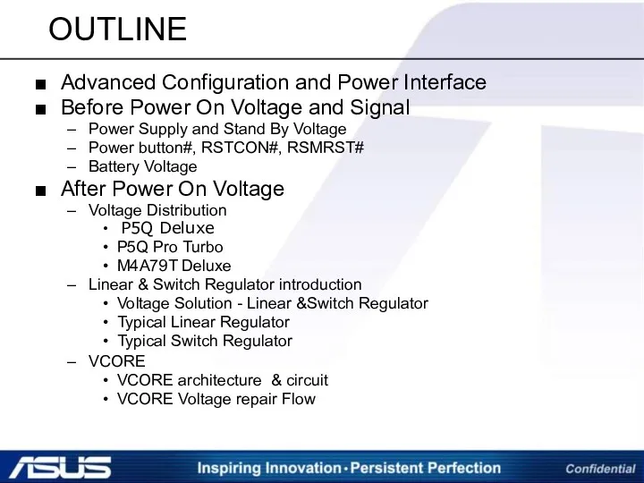
OUTLINE
Advanced Configuration and Power Interface
Before Power On Voltage and Signal
Power Supply
OUTLINE
Advanced Configuration and Power Interface
Before Power On Voltage and Signal
Power Supply
Advanced Configuration
and
Power Interface
Advanced Configuration
and
Power Interface
Advanced Configuration and Power Interface
S0: All Power
S3: Standby and Dual
S5: Only
Advanced Configuration and Power Interface
S0: All Power
S3: Standby and Dual
S5: Only
Before Power On
Voltage and Signal
Before Power On
Voltage and Signal
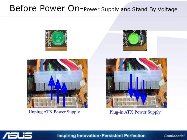
Before Power On-Power Supply and Stand By Voltage
Before Power On-Power Supply and Stand By Voltage
Before Power On-Power Supply and Stand By Voltage
PS-ON# is an active
Before Power On-Power Supply and Stand By Voltage
PS-ON# is an active
Before Power On-Power Supply and Stand By Voltage
Before Power On-Power Supply and Stand By Voltage
Before Power On-Power Supply and Stand By Voltage
Before you turn on
Before Power On-Power Supply and Stand By Voltage
Before you turn on
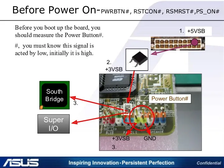
Before Power On-PWRBTN#, RSTCON#, RSMRST#,PS_ON#
+3VSB
GND
+5VSB
+3VSB
1.
2.
3.
3.
Super I/O
Power Button#
Before you boot up the
Before Power On-PWRBTN#, RSTCON#, RSMRST#,PS_ON#
+3VSB
GND
+5VSB
+3VSB
1.
2.
3.
3.
Super I/O
Power Button#
Before you boot up the
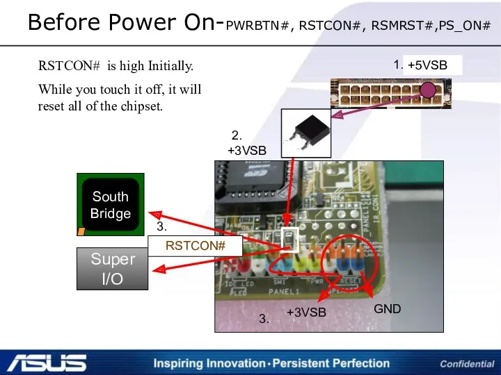
Before Power On-PWRBTN#, RSTCON#, RSMRST#,PS_ON#
+3VSB
GND
+5VSB
+3VSB
1.
2.
3.
3.
Super I/O
RSTCON#
RSTCON# is high Initially.
While you
Before Power On-PWRBTN#, RSTCON#, RSMRST#,PS_ON#
+3VSB
GND
+5VSB
+3VSB
1.
2.
3.
3.
Super I/O
RSTCON#
RSTCON# is high Initially.
While you
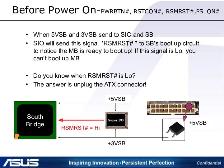
Before Power On-PWRBTN#, RSTCON#, RSMRST#,PS_ON#
When 5VSB and 3VSB send to SIO
Before Power On-PWRBTN#, RSTCON#, RSMRST#,PS_ON#
When 5VSB and 3VSB send to SIO
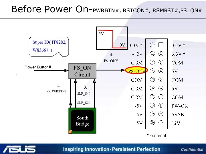
Before Power On-PWRBTN#, RSTCON#, RSMRST#,PS_ON#
Power Button#
Before Power On-PWRBTN#, RSTCON#, RSMRST#,PS_ON#
Power Button#
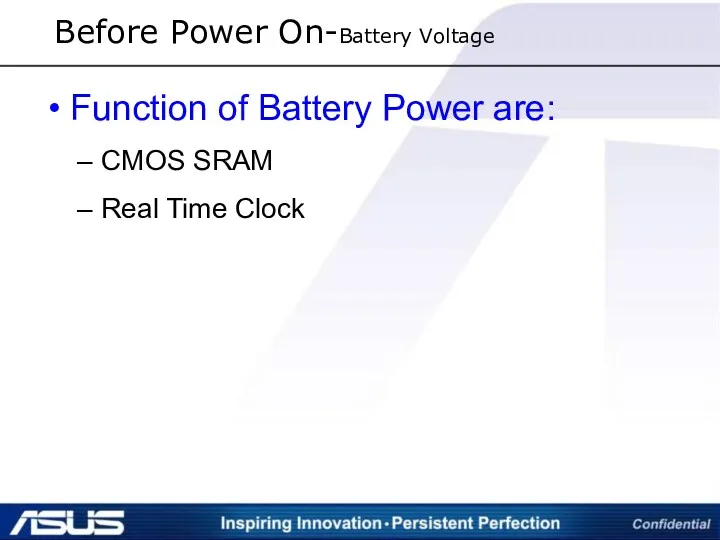
Before Power On-Battery Voltage
Function of Battery Power are:
CMOS SRAM
Real Time Clock
Before Power On-Battery Voltage
Function of Battery Power are:
CMOS SRAM
Real Time Clock
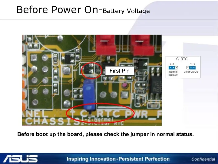
Before Power On-Battery Voltage
Before boot up the board, please check the
Before Power On-Battery Voltage
Before boot up the board, please check the
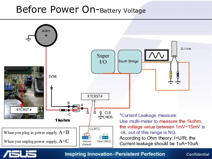
Before Power On-Battery Voltage
South Bridge
+
3VSB
Battery
RTCRST#
32.7 KHz
CLR CMOS
1kohm
*Current Leakage measure:
Use multi-meter
Before Power On-Battery Voltage
South Bridge
+
3VSB
Battery
RTCRST#
32.7 KHz
CLR CMOS
1kohm
*Current Leakage measure:
Use multi-meter
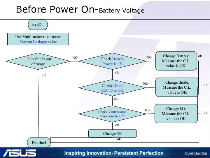
Before Power On-Battery Voltage
Use Multi-meter to measure
Current Leakage value
START
Check Vbatt related
Before Power On-Battery Voltage
Use Multi-meter to measure
Current Leakage value
START
Check Vbatt related
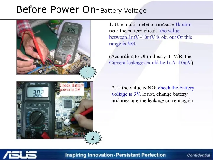
Before Power On-Battery Voltage
1
1. Use multi-meter to measure 1k ohm near
Before Power On-Battery Voltage
1
1. Use multi-meter to measure 1k ohm near
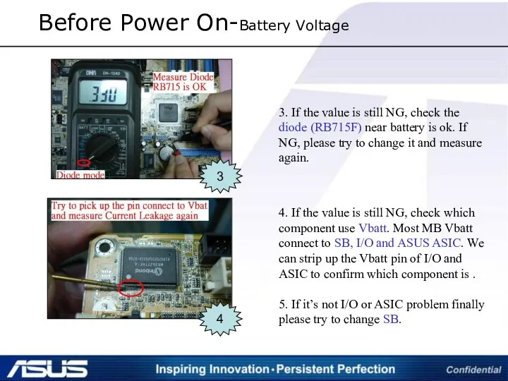
Before Power On-Battery Voltage
3
3. If the value is still NG, check
Before Power On-Battery Voltage
3
3. If the value is still NG, check
AFTER POWER ON VOLTAGE
AFTER POWER ON VOLTAGE
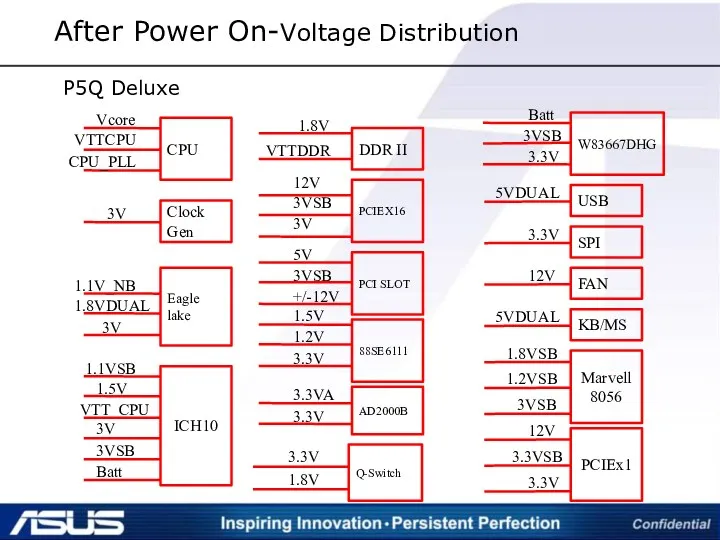
After Power On-Voltage Distribution
After Power On-Voltage Distribution
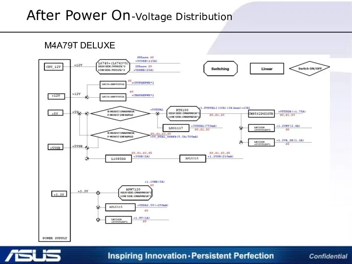
After Power On-Voltage Distribution
M4A79T DELUXE
After Power On-Voltage Distribution
M4A79T DELUXE
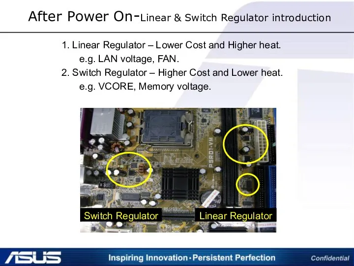
After Power On-Linear & Switch Regulator introduction
1. Linear Regulator –
After Power On-Linear & Switch Regulator introduction
1. Linear Regulator –
After Power On-Linear & Switch Regulator introduction
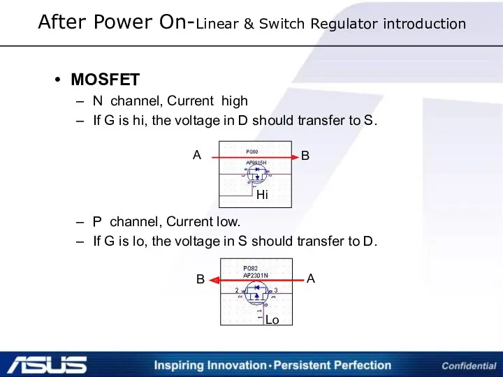
MOSFET
N channel, Current
After Power On-Linear & Switch Regulator introduction
MOSFET
N channel, Current
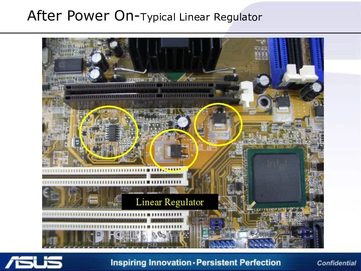
After Power On-Typical Linear Regulator
After Power On-Typical Linear Regulator
After Power On-Typical Linear Regulator
LM324 Diagrams
Power Amplifier
Operational Amplifiers
Reference voltage
After Power On-Typical Linear Regulator
LM324 Diagrams
Power Amplifier
Operational Amplifiers
Reference voltage
IN+ = IN-, +1.5VSB REF (12th pin)= +1.5VSB FB (13th pin)
If
IN+ = IN-, +1.5VSB REF (12th pin)= +1.5VSB FB (13th pin)
If
After Power On-Typical Switch Regulator
After Power On-Typical Switch Regulator
After Power On-Typical Switch Regulator
After Power On-Typical Switch Regulator
After Power On-Typical Switch Regulator
After Power On-Typical Switch Regulator

VCORE
VCORE
After Power On-VCORE architecture & circuit
After Power On-VCORE architecture & circuit
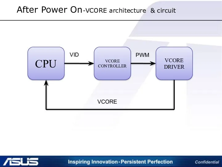
VID
PWM
VCORE
After Power On-VCORE architecture & circuit
VID
PWM
VCORE
After Power On-VCORE architecture & circuit
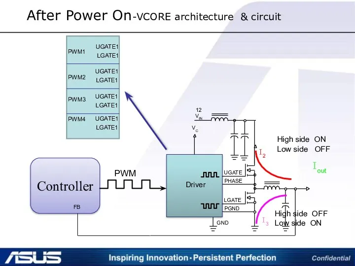
After Power On-VCORE architecture & circuit
PWM
After Power On-VCORE architecture & circuit
PWM
VID
PWM
VCORE Control IC—ADP3180
After Power On-VCORE architecture & circuit
VID
PWM
VCORE Control IC—ADP3180
After Power On-VCORE architecture & circuit
After Power On-VCORE architecture & circuit
After Power On-VCORE architecture & circuit
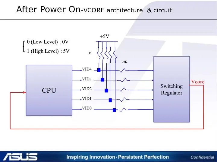
CPU
VID4
VID3
VID2
VID1
VID0
+5V
1K
10K
Switching
Regulator
Vcore
0 (Low Level) :0V
1 (High Level) :5V
After Power On-VCORE architecture &
CPU
VID4
VID3
VID2
VID1
VID0
+5V
1K
10K
Switching
Regulator
Vcore
0 (Low Level) :0V
1 (High Level) :5V
After Power On-VCORE architecture &
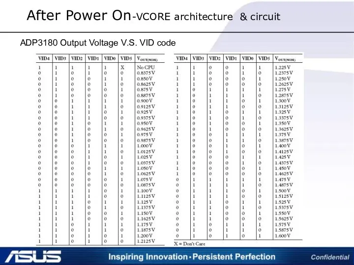
ADP3180 Output Voltage V.S. VID code
After Power On-VCORE architecture & circuit
ADP3180 Output Voltage V.S. VID code
After Power On-VCORE architecture & circuit
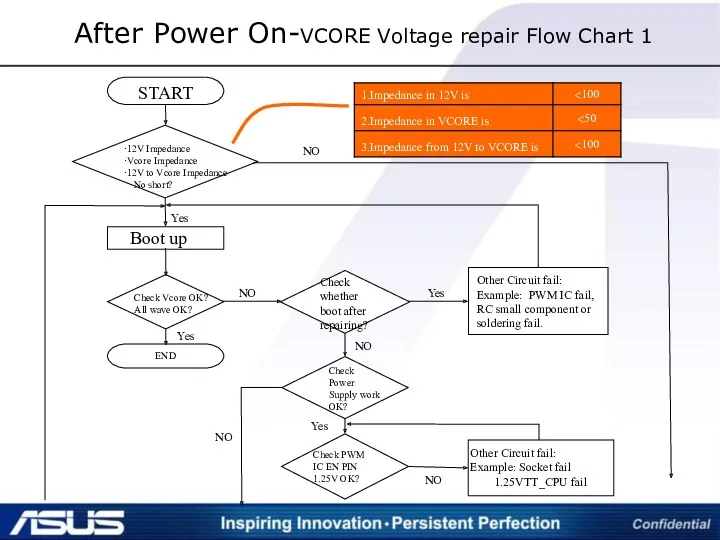
After Power On-VCORE Voltage repair Flow Chart 1
After Power On-VCORE Voltage repair Flow Chart 1
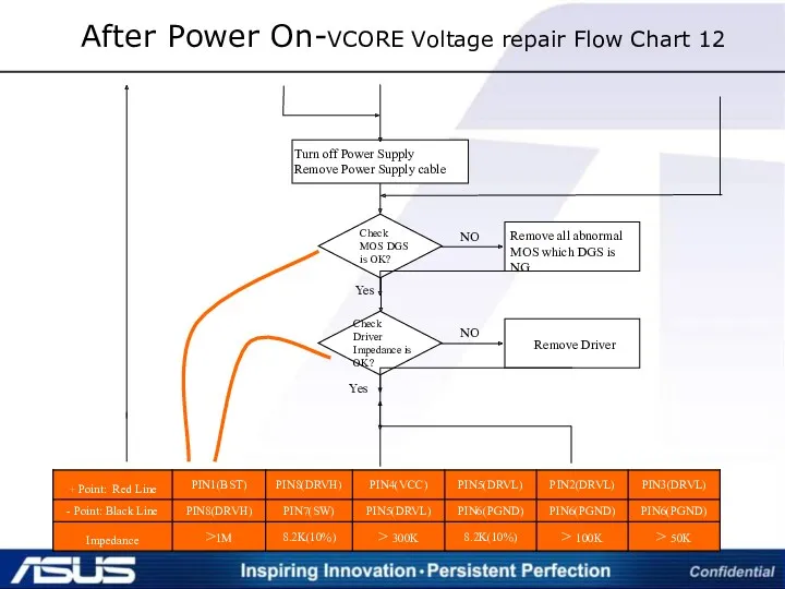
Turn off Power Supply
Remove Power Supply cable
NO
Remove all abnormal MOS which
Turn off Power Supply
Remove Power Supply cable
NO
Remove all abnormal MOS which
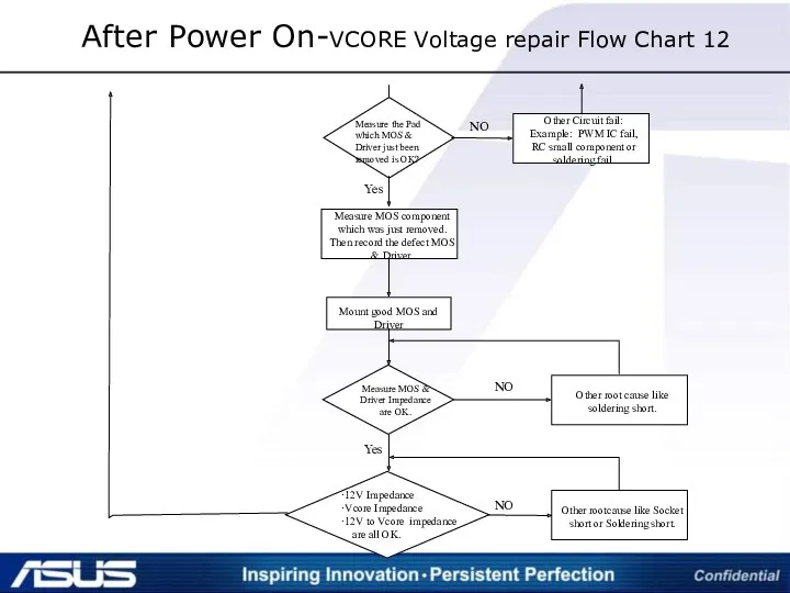
Mount good MOS and Driver
Other root cause like soldering short.
NO
Other rootcause
Mount good MOS and Driver
Other root cause like soldering short.
NO
Other rootcause
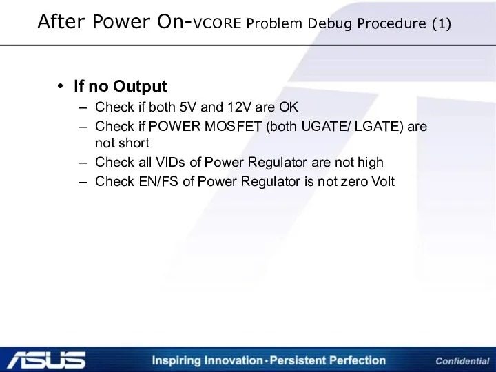
After Power On-VCORE Problem Debug Procedure (1)
If no Output
Check if both
After Power On-VCORE Problem Debug Procedure (1)
If no Output
Check if both
If the output voltage wrong
Check if VIDs of Power Regulator are
If the output voltage wrong
Check if VIDs of Power Regulator are
 С праздником весны!
 Мультимедийная презентация на тему Насколько велик моль?
 презентация по ОРКСЭ 4 класс
 Презентация проекта Весёлые ручки
 Химическая организация клетки. Неорганические вещества
 Взаимное расположение графиков линейной функции
 1959 оной гахай жэлээхид та бугэдэниие Сагаан hараар, сагаалганаар амаршална
 О родных и близких людях с любовью
 Презентация к празднику Свет родных берёз
 Фасовочно-упаковочное оборудование
 Справочно-правовая система (СПС) Консультант плюс
 Вышивка
 Презентация Путешествие в сказку золотая Хохлома
 9 мая 1945 – День Победы
 Частотные преобразователи
 Презентация к уроку окружающего мира Чтобы путь был счастливым 3 класс
 Счет
Счет Электрические машины
 Опытно-промышленное предприятие кучного выщелачивания на месторождении Лунное
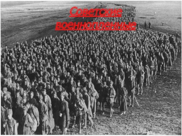 Советские военнопленные
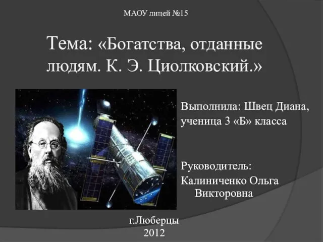 Богатства, отданные людям. К. Э. Циолковский
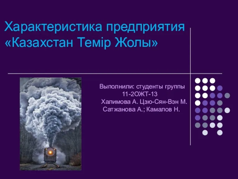 Характеристика предприятия Казахстан Темiр Жолы
 Острое аномальное маточное кровотечение
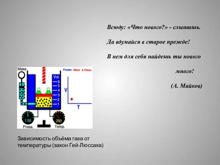 Молярный объем газов
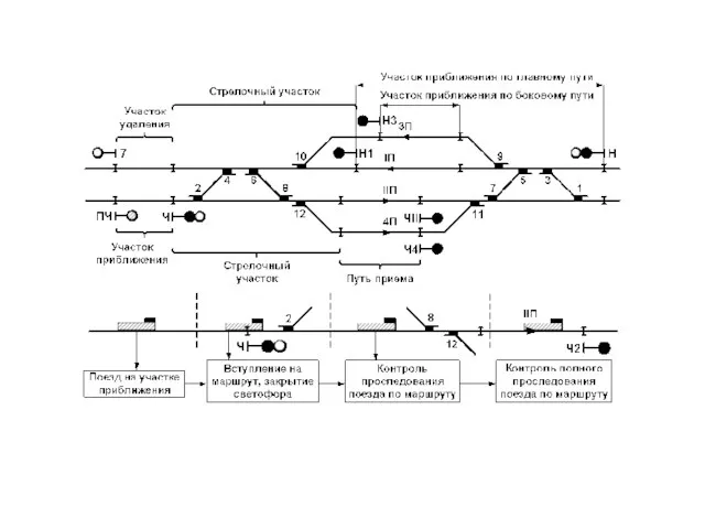 Станционная система АиТ на железной дороге
 Цисар Маргарита - (К.1) - Красноарм. - Презентация
 Государственные должности и должности государственной службы
 Презентация к интегрированной интеллектуальной игре по биологии и химииВодный мир. 8 класс.