- Programmable Logic and FPGA

Содержание
- 2. Objectives What is a programmable logic What is an FPGA Structure Special functions Comparison and Usages
- 3. Semiconductor Chips FPGA & CPLD ASICs Application Specific Integrated Circuits Microprocessors Microcontrollers
- 4. Programmable logic An integrated circuit that can be programmed/reprogrammed with a digital logic of a curtain
- 5. Advantages Short Development time Reconfigurable Saves board space Flexible to changes No need for ASIC expensive
- 6. How it Began : PLA Programmable Logic Array First programmable device 2-level and-or structure One time
- 7. SPLD - CPLD Simple Programmable logic device Single AND Level Flip-Flops and feedbacks Complex Programmable logic
- 8. FPGA - Field Programmable Gate Array Programmable logic blocks (Logic Element “LE”) Implement combinatorial and sequential
- 9. Configuring LUT Required Function Truth Table Programmed LUT LUT is a RAM with data width of
- 10. Special FPGA functions Internal SRAM Embedded Multipliers and DSP blocks Embedded logic analyzer Embedded CPUs High
- 11. Comparison
- 12. Usages Digital designs where ASIC is not commercial Reconfigurable systems Upgradeable systems ASIC prototyping and emulation
- 13. Manufacturers Xilinx Altera Lattice Actel We will work with Altera FPGAs
- 14. Cyclone II - 20 18,752 LEs 52 M4K RAM blocks 240K total RAM bits 52 9x9
- 15. Cyclone II Internals Logic Array M4K Memory Blocks Embedded Multipliers Phase-Locked Loops I/O Elements
- 16. Cyclone II Logic Array Build of LABs (logic array blocks) and reconfigurable interconnect
- 17. Cyclone II Logic Array Block (LAB) 16 LEs Local Interconnect LE carry chains Register chains LAB
- 18. Cyclone II Logic Element (LE)
- 19. LE in Normal Mode Suitable for general logic applications and combinational functions.
- 20. LE in Arithmetic Mode Ideal for implementing adders, counters, accumulators, and comparators.
- 21. Cyclone II I/O Features In/Out/Tri-state Different Voltages and I/O Standards Flip-flop option Pull-up resistors DDR interface
- 22. Cyclone II I/O Buffer
- 23. Cyclone II Clocking 16 Global Clocks 4 PLLs
- 24. Cyclone II PLL 3 Outputs Clock Division Clock Multiplication Phase shift
- 25. Memory True Dual port RAM/ROM with dual clock Variable data width 4K×1, 2K×2, 1K×4, 512×8, 512×9,
- 26. Cyclone II Memory Structure
- 27. Cyclone II Multipliers 18x18 or 2 9x9 modes Up to 250MHz Performance
- 28. Delays and maximal frequency Gate delay – Delay of logic element DFF delay tco (tsu -
- 29. Design flow
- 30. Design Rules
- 32. Скачать презентацию

Objectives
What is a programmable logic
What is an FPGA
Structure
Special functions
Comparison and Usages
Altera
Objectives
What is a programmable logic
What is an FPGA
Structure
Special functions
Comparison and Usages
Altera

Semiconductor Chips
FPGA & CPLD
ASICs
Application Specific
Integrated Circuits
Microprocessors
Microcontrollers
Semiconductor Chips
FPGA & CPLD
ASICs
Application Specific
Integrated Circuits
Microprocessors
Microcontrollers

Programmable logic
An integrated circuit that can be programmed/reprogrammed with a digital
Programmable logic
An integrated circuit that can be programmed/reprogrammed with a digital

Advantages
Short Development time
Reconfigurable
Saves board space
Flexible to changes
No need for ASIC expensive
Advantages
Short Development time
Reconfigurable
Saves board space
Flexible to changes
No need for ASIC expensive

How it Began : PLA
Programmable Logic Array
First programmable device
2-level and-or
How it Began : PLA
Programmable Logic Array
First programmable device
2-level and-or

SPLD - CPLD
Simple Programmable logic device
Single AND Level
Flip-Flops and feedbacks
Complex Programmable
SPLD - CPLD
Simple Programmable logic device
Single AND Level
Flip-Flops and feedbacks
Complex Programmable

FPGA - Field Programmable Gate Array
Programmable logic blocks (Logic Element “LE”)
Implement
FPGA - Field Programmable Gate Array
Programmable logic blocks (Logic Element “LE”) Implement

Configuring LUT
Required Function
Truth Table
Programmed LUT
LUT is a RAM with data width
Configuring LUT
Required Function
Truth Table
Programmed LUT
LUT is a RAM with data width

Special FPGA functions
Internal SRAM
Embedded Multipliers
and DSP blocks
Embedded logic analyzer
Embedded CPUs
High
Special FPGA functions
Internal SRAM
Embedded Multipliers
and DSP blocks
Embedded logic analyzer
Embedded CPUs
High

Comparison
Comparison

Usages
Digital designs where ASIC is not commercial
Reconfigurable systems
Upgradeable systems
ASIC prototyping and
Usages
Digital designs where ASIC is not commercial
Reconfigurable systems
Upgradeable systems
ASIC prototyping and

Manufacturers
Xilinx
Altera
Lattice
Actel
We will work with Altera FPGAs
Manufacturers
Xilinx
Altera
Lattice
Actel
We will work with Altera FPGAs

Cyclone II - 20
18,752 LEs
52 M4K RAM blocks
240K total
Cyclone II - 20
18,752 LEs
52 M4K RAM blocks
240K total

Cyclone II Internals
Logic Array
M4K Memory
Blocks
Embedded
Multipliers
Phase-Locked
Loops
I/O
Elements
Cyclone II Internals
Logic Array
M4K Memory
Blocks
Embedded
Multipliers
Phase-Locked
Loops
I/O
Elements

Cyclone II Logic Array
Build of LABs (logic array blocks) and reconfigurable
Cyclone II Logic Array
Build of LABs (logic array blocks) and reconfigurable

Cyclone II Logic Array Block (LAB)
16 LEs
Local Interconnect
LE carry chains
Register chains
LAB
Cyclone II Logic Array Block (LAB)
16 LEs
Local Interconnect
LE carry chains
Register chains
LAB

Cyclone II Logic Element (LE)
Cyclone II Logic Element (LE)

LE in Normal Mode
Suitable for general logic applications and combinational functions.
LE in Normal Mode
Suitable for general logic applications and combinational functions.

LE in Arithmetic Mode
Ideal for implementing adders, counters, accumulators, and comparators.
LE in Arithmetic Mode
Ideal for implementing adders, counters, accumulators, and comparators.

Cyclone II I/O Features
In/Out/Tri-state
Different Voltages and I/O Standards
Flip-flop option
Pull-up resistors
DDR interface
Series
Cyclone II I/O Features
In/Out/Tri-state
Different Voltages and I/O Standards
Flip-flop option
Pull-up resistors
DDR interface
Series

Cyclone II I/O Buffer
Cyclone II I/O Buffer

Cyclone II Clocking
16 Global Clocks
4 PLLs
Cyclone II Clocking
16 Global Clocks
4 PLLs

Cyclone II PLL
3 Outputs
Clock Division
Clock Multiplication
Phase shift
Cyclone II PLL
3 Outputs
Clock Division
Clock Multiplication
Phase shift

Memory
True Dual port RAM/ROM with dual clock
Variable data width
4K×1, 2K×2,
Memory
True Dual port RAM/ROM with dual clock
Variable data width
4K×1, 2K×2,

Cyclone II Memory Structure
Cyclone II Memory Structure

Cyclone II Multipliers
18x18 or 2 9x9 modes
Up to 250MHz Performance
Cyclone II Multipliers
18x18 or 2 9x9 modes
Up to 250MHz Performance

Delays and maximal frequency
Gate delay – Delay of logic element
DFF
Delays and maximal frequency
Gate delay – Delay of logic element
DFF

Design flow
Design flow

Design Rules
Design Rules
 Современная модель технологической подготовки школьников
 В здоровом теле здоровый дух. Соревнования
 Мікропроцесорна техніка
 Медицинская статистика. Определение, задачи, разделы
 Республика Крым
 Блокированный дом на 2 семьи
 Дробно рациональные уравнения
 Методическая копилка
 Сільське господарство України. Рослинництво
 20240124_izo_7_klass._tema_4._tsvet_-_element_kompozitsionnogo_tvorchestva
 Строительная геотехнология
 Правовые основы преподавания религий и этики в школе
 Евангельские события Рождества Христова
 Преподобный Серафим Саровский
 Психологическое консультирование
 Афанасий Фет. Особенности лирики поэта. Философская лирика
 Комплексная оценка состояния здоровья ребенка
 Оценивание личностных достижений учащихся при обучении химии в 8 классе общеобразовательной школы
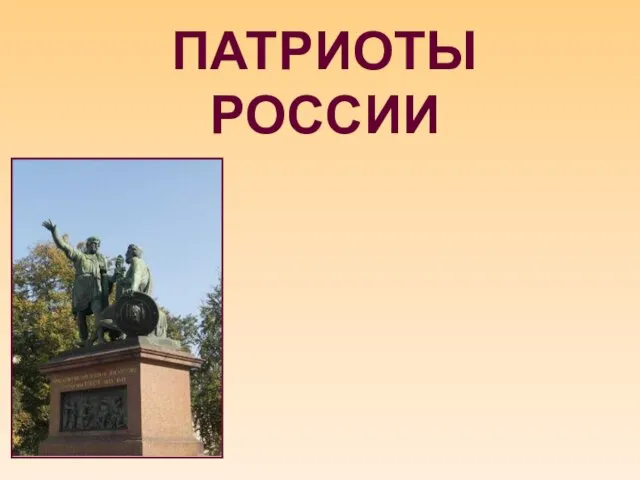 Патриоты России
 Значение дидактической игры в экологическом воспитании детей.
 Закономерности наследования признаков
 Технология установки дополнительного света на легковых автомобилях в соответствии с техническим регламентом таможенного союза
 ОТКРЫТЫЙ УРОК ПО ХИМИИ 8 КЛАСС
 Самопрезентация: Применение современных методов обучения как средства повышения эффективности в изучении истории и обществознания.
 Знакомство с Arduino. Lesson 1
 Студенческие научные кружки
 Пасха Христова
 Правила технической эксплуатации железных дорог Российской Федерации