- Topology Swapping for Switchers - Sanjaya Maniktala

Содержание
- 2. A Switcher is a Switcher is a Switcher A switcher IC is basically this: A switch
- 3. Understanding what is ‘Ground’ (+ve to +ve Configuration)
- 4. -ve to -ve Configuration
- 5. -ve to +ve Configuration
- 6. +ve to -ve Configuration
- 7. -ve to +ve Configuration (redrawn)
- 8. +ve to -ve Configuration (redrawn)
- 9. What about the IC Ground? In fact there are so many definitions of ‘Ground’ that it
- 10. The ‘N-switch’ and the ‘P-switch’ Turning it ON
- 11. The ‘N-switch’ and the ‘P-switch’ Turning it OFF
- 12. The ‘LSD’ Cell
- 13. The terminology If the cathode of the diode connects to the LSD node: call it a
- 14. Lookup Table for LSD Descriptors
- 15. What are configurations? The words ‘step-down’ (Buck) or ‘step-up’ (Boost) or ‘step up/down’ (Buck-Boost) merely refer
- 16. Buck-Boost Configurations The Buck-Boost will take a given voltage and change it to either a smaller
- 17. Buck Configurations
- 18. Boost Configurations
- 19. Buck-Boost Configurations
- 20. N-Switch Configurations to P-Switch Configurations To draw the negative ground circuit from a positive ground circuit
- 21. ‘Inversion’
- 22. An example of ‘Inversion’
- 23. Why study the IC Construction? Having understood the topologies and their configurations, it is important to
- 24. Type 1 IC (“Boost/Buck-Boost IC”)
- 25. Type 2 IC (“Buck IC”)
- 26. Summary of IC differences (1) Type 1 connects the Source/Emitter (lower voltage switch pin) to the
- 27. Summary of IC differences (2) NPN switches are generally easier to drive since the Base has
- 28. LM1575/2575 This is a Type 2 IC by our definition. Note that the NPN can be
- 29. LM2590HV This is a Type 2 IC by our definition. Note that the NPN can be
- 30. Type 2 IC’s with NPN Switches We see that the ‘drop’ across the switch is uniformly
- 31. LM2670 This is a Type 2 IC by our definition. Note that the N-Fet has to
- 32. Summary of IC differences (3) Returning to N-switches, we can conclude that despite their advantages, the
- 33. A ‘Boost IC’: the LM2577 This is a Boost application. So can IC this do Buck-Boost/Flyback????
- 34. LM2577 as a Flyback So why wasn’t this obvious right away???
- 35. LM2577: The Block Diagram Not very obvious, but this is a Type 1 IC!
- 36. LM1578/2578/3578 The transistor is completely uncommitted
- 37. LM1578 Applications From L to R: Pinout, +ve to +ve Boost, +ve to +ve Buck
- 38. Labeling of Pins Don’t be confused by the pin labels. There is unfortunately no uniformity. Different
- 39. How is a Boost different from a Buck-Boost? Apply D=0.6 and see what happens for each
- 40. Boost and Buck-Boost compared The main difference is in the feedback. Since for a Boost, the
- 41. Nomenclature used In this article we will use the word ‘Flyback’ to refer exclusively to a
- 42. Boost/Buck-Boost/what else??
- 43. Now the crucial chain of logic behind hidden applications: the primary intended application for the Type
- 44. Natural Choices of a Type 1 IC a) Positive to Positive Boost: Uses a Type B
- 45. (Type B LSD Cell, Type 1 IC) +ve to +ve Boost
- 46. (Type B LSD Cell, Type 1 IC) -ve to +ve Buck-Boost
- 47. (Type B LSD Cell, Type 1 IC) -ve to -ve Buck
- 48. (Type A LSD Cell, Type 1 IC) -ve to -ve Boost
- 49. (Type A LSD Cell, Type 1 IC) +ve to -ve Buck-Boost
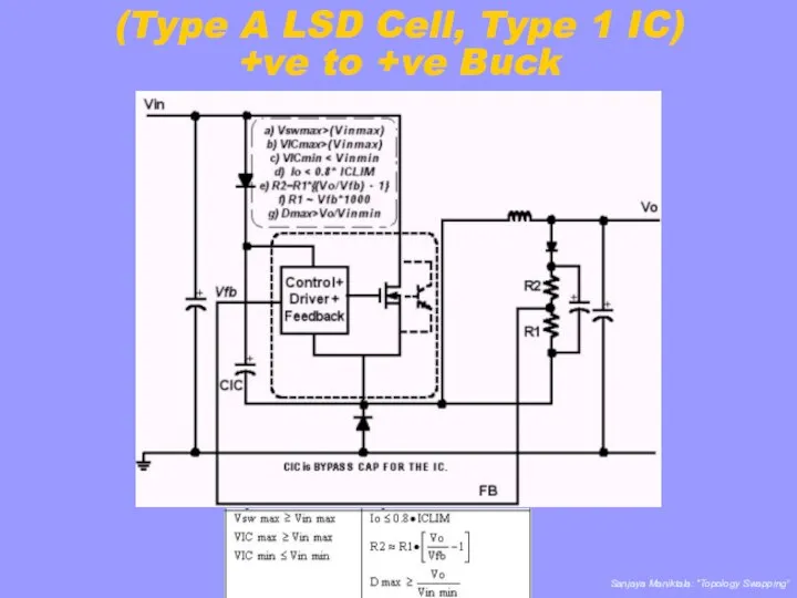
- 50. (Type A LSD Cell, Type 1 IC) +ve to +ve Buck
- 51. Summary of Type 1 IC Applications
- 52. Natural Choices of a Type 2 IC a) Positive to Positive Buck: Uses a Type A
- 53. (Type A LSD Cell, Type 2 IC) +ve to +ve Buck
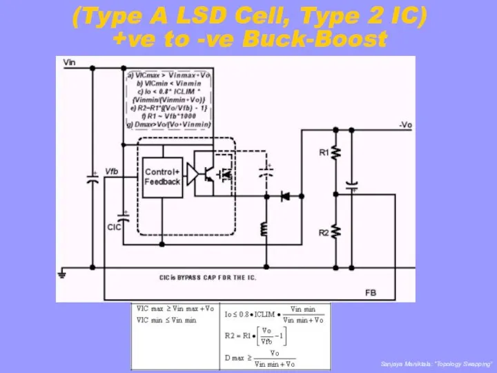
- 54. (Type A LSD Cell, Type 2 IC) +ve to -ve Buck-Boost
- 55. (Type A LSD Cell, Type 2 IC) -ve to -ve Boost
- 56. ‘Forced’ Choices for Type 2 IC? Because the Drain/Collector is NOT uncommitted, it is not possible
- 57. Summary of Type 2 IC Applications
- 58. Transformer-based Type 1 Applications (1)
- 59. Transformer-based Type 1 Applications (2)
- 60. Differential Sensing Techniques (1)
- 61. Differential Sensing Techniques (2)
- 62. Equations for Differential Sense
- 63. Summary of Applications
- 64. Example 1 The LM2585 is a ‘3A Flyback regulator’. Can it be used in a Boost
- 65. Example 1 (contd) This is the checklist. We see that the input voltage must be below
- 66. Example 2 The required application conditions are Vin ranging from 4.5V to 5.5V. The output requirement
- 67. Example 2 (contd) Referring to the datasheet of this device we get : VICmin=4V,VICmax=14V ICLIM=1.55A. Dmax
- 68. Nuances of Topology Swapping One of the main concerns when we jump topologies has to do
- 69. Conquering the RHP Zero (1)
- 70. Conquering the RHP Zero (2)
- 72. Скачать презентацию
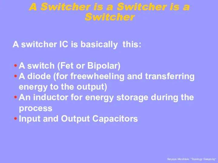
A Switcher is a Switcher is a Switcher
A switcher IC is
A Switcher is a Switcher is a Switcher
A switcher IC is
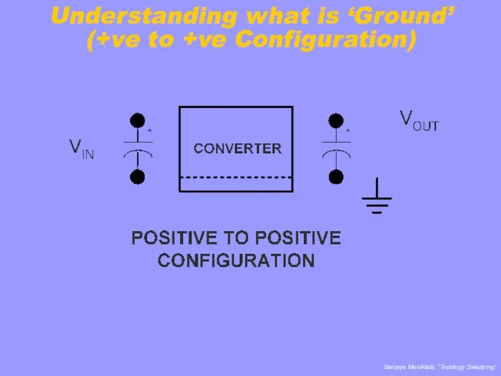
Understanding what is ‘Ground’
(+ve to +ve Configuration)
Understanding what is ‘Ground’
(+ve to +ve Configuration)
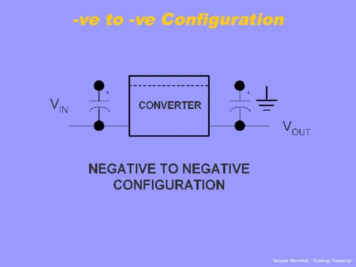
-ve to -ve Configuration
-ve to -ve Configuration
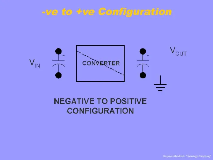
-ve to +ve Configuration
-ve to +ve Configuration
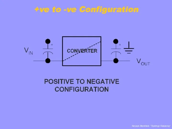
+ve to -ve Configuration
+ve to -ve Configuration
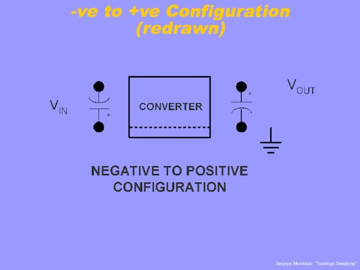
-ve to +ve Configuration
(redrawn)
-ve to +ve Configuration
(redrawn)
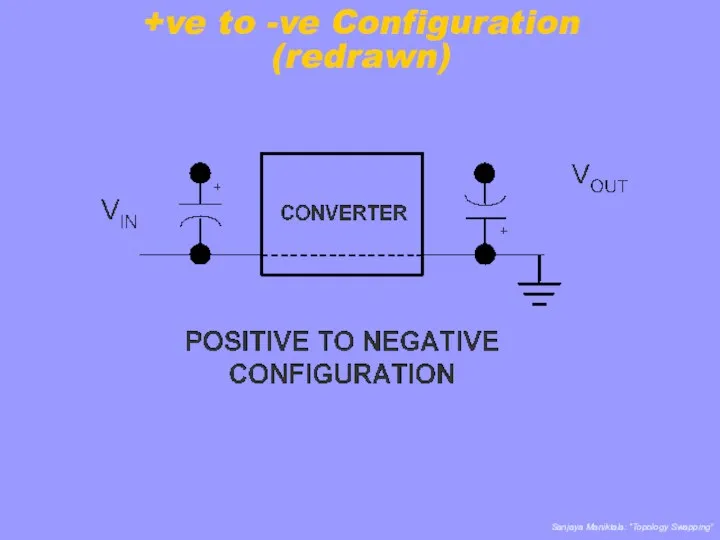
+ve to -ve Configuration
(redrawn)
+ve to -ve Configuration
(redrawn)
What about the IC Ground?
In fact there are so many definitions
What about the IC Ground?
In fact there are so many definitions
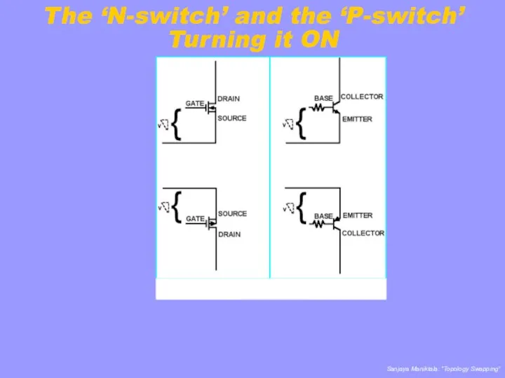
The ‘N-switch’ and the ‘P-switch’
Turning it ON
The ‘N-switch’ and the ‘P-switch’
Turning it ON
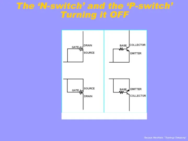
The ‘N-switch’ and the ‘P-switch’
Turning it OFF
The ‘N-switch’ and the ‘P-switch’
Turning it OFF
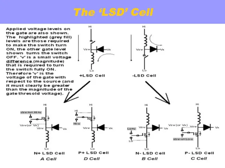
The ‘LSD’ Cell
The ‘LSD’ Cell
The terminology
If the cathode of the diode connects to the LSD
The terminology
If the cathode of the diode connects to the LSD
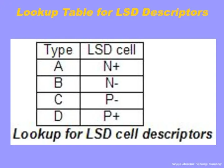
Lookup Table for LSD Descriptors
Lookup Table for LSD Descriptors
What are configurations?
The words ‘step-down’ (Buck) or ‘step-up’ (Boost) or ‘step
What are configurations?
The words ‘step-down’ (Buck) or ‘step-up’ (Boost) or ‘step
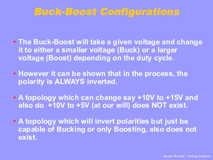
Buck-Boost Configurations
The Buck-Boost will take a given voltage and change it
Buck-Boost Configurations
The Buck-Boost will take a given voltage and change it
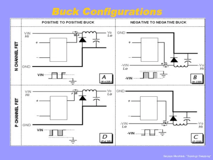
Buck Configurations
Buck Configurations
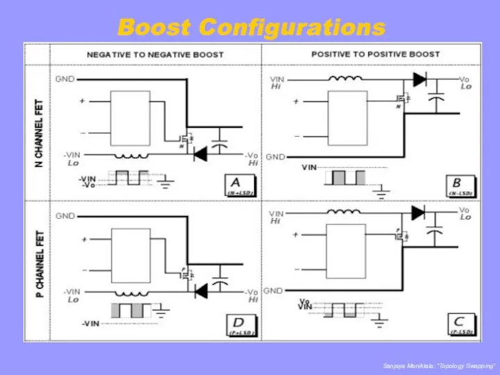
Boost Configurations
Boost Configurations
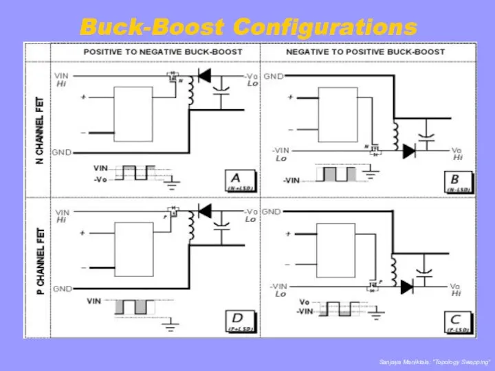
Buck-Boost Configurations
Buck-Boost Configurations
N-Switch Configurations to P-Switch Configurations
To draw the negative ground circuit
N-Switch Configurations to P-Switch Configurations
To draw the negative ground circuit
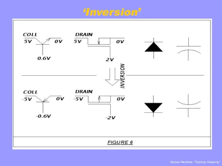
‘Inversion’
‘Inversion’
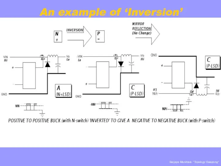
An example of ‘Inversion’
An example of ‘Inversion’
Why study the IC Construction?
Having understood the topologies and their
Why study the IC Construction?
Having understood the topologies and their
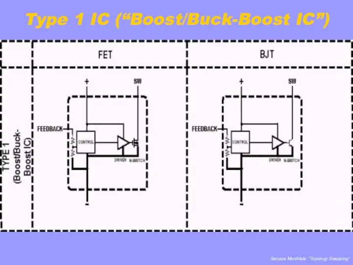
Type 1 IC (“Boost/Buck-Boost IC”)
Type 1 IC (“Boost/Buck-Boost IC”)
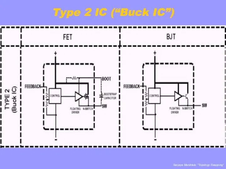
Type 2 IC (“Buck IC”)
Type 2 IC (“Buck IC”)
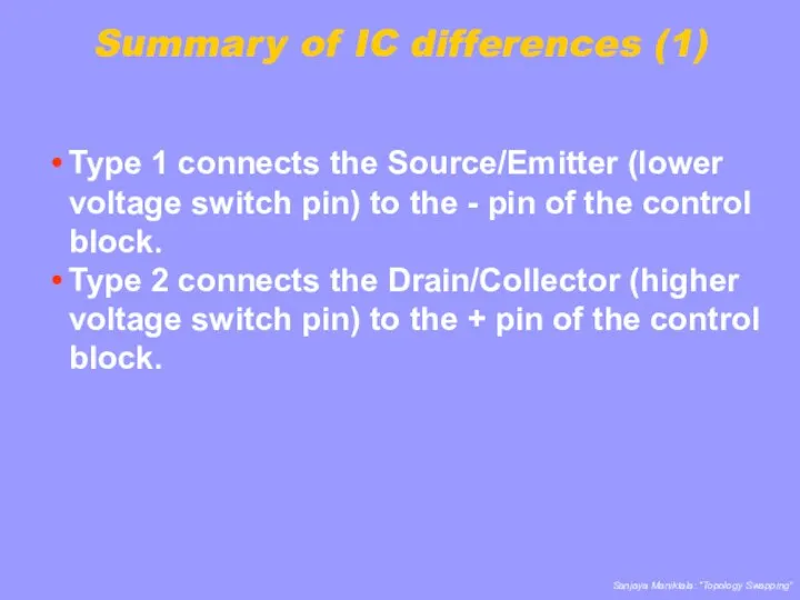
Summary of IC differences (1)
Type 1 connects the Source/Emitter (lower voltage
Summary of IC differences (1)
Type 1 connects the Source/Emitter (lower voltage
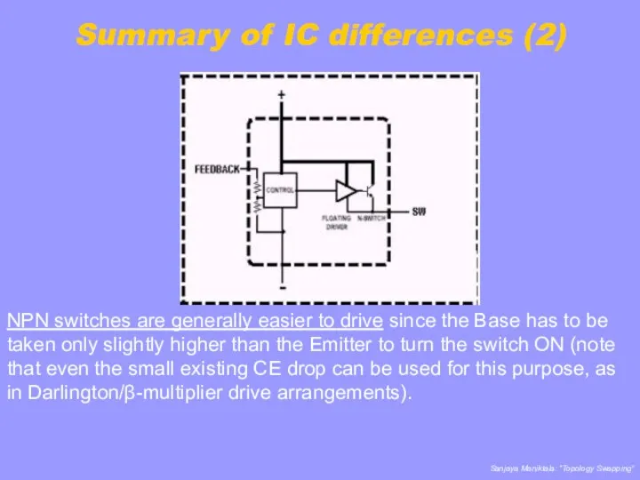
Summary of IC differences (2)
NPN switches are generally easier to drive
Summary of IC differences (2)
NPN switches are generally easier to drive
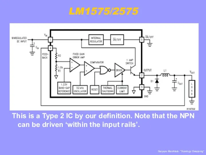
LM1575/2575
This is a Type 2 IC by our definition. Note that
LM1575/2575
This is a Type 2 IC by our definition. Note that
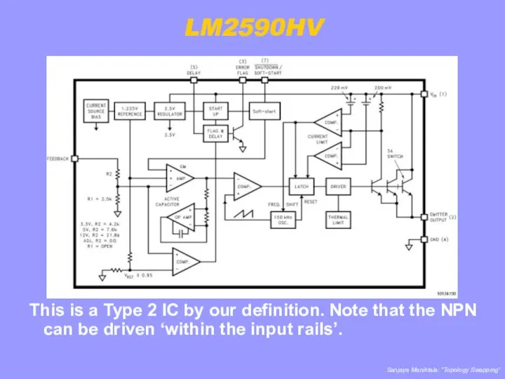
LM2590HV
This is a Type 2 IC by our definition. Note that
LM2590HV
This is a Type 2 IC by our definition. Note that
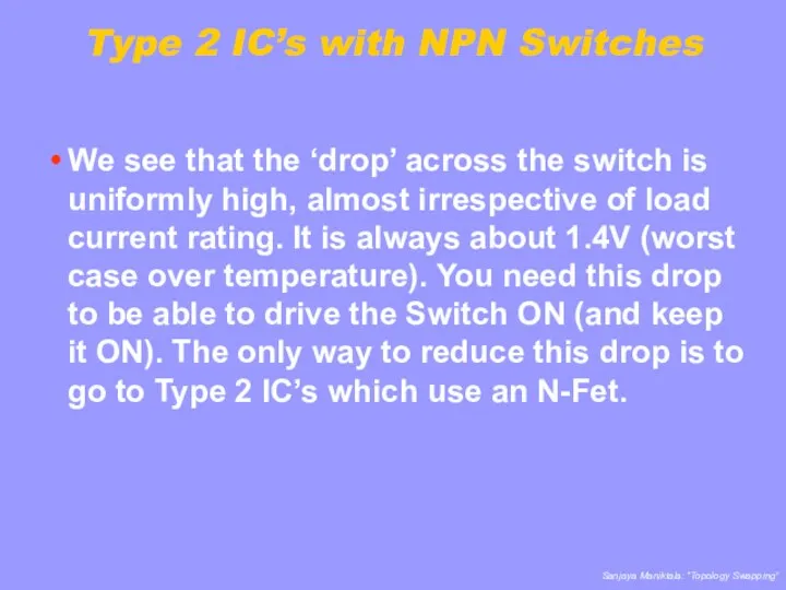
Type 2 IC’s with NPN Switches
We see that the ‘drop’ across
Type 2 IC’s with NPN Switches
We see that the ‘drop’ across
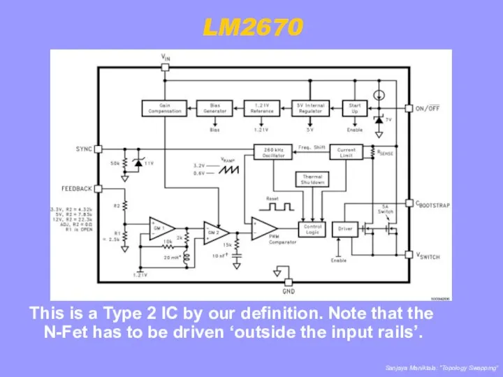
LM2670
This is a Type 2 IC by our definition. Note that
LM2670
This is a Type 2 IC by our definition. Note that
Summary of IC differences (3)
Returning to N-switches, we can conclude that
Summary of IC differences (3)
Returning to N-switches, we can conclude that
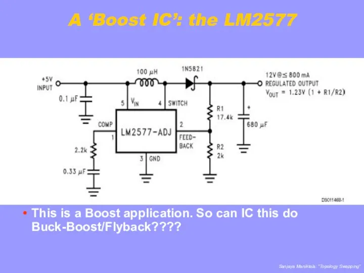
A ‘Boost IC’: the LM2577
This is a Boost application. So can
A ‘Boost IC’: the LM2577
This is a Boost application. So can
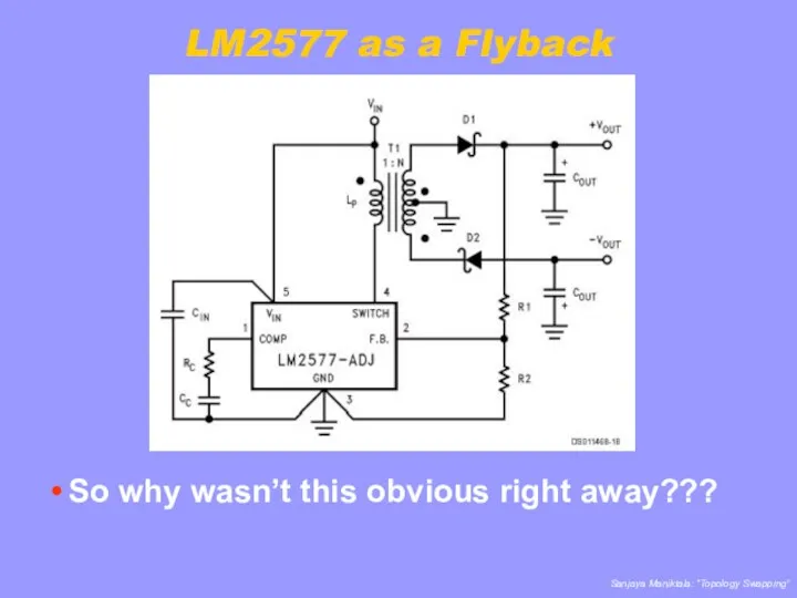
LM2577 as a Flyback
So why wasn’t this obvious right away???
LM2577 as a Flyback
So why wasn’t this obvious right away???
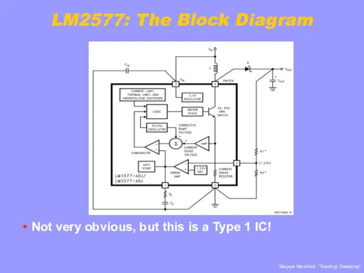
LM2577: The Block Diagram
Not very obvious, but this is a Type
LM2577: The Block Diagram
Not very obvious, but this is a Type
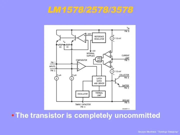
LM1578/2578/3578
The transistor is completely uncommitted
LM1578/2578/3578
The transistor is completely uncommitted
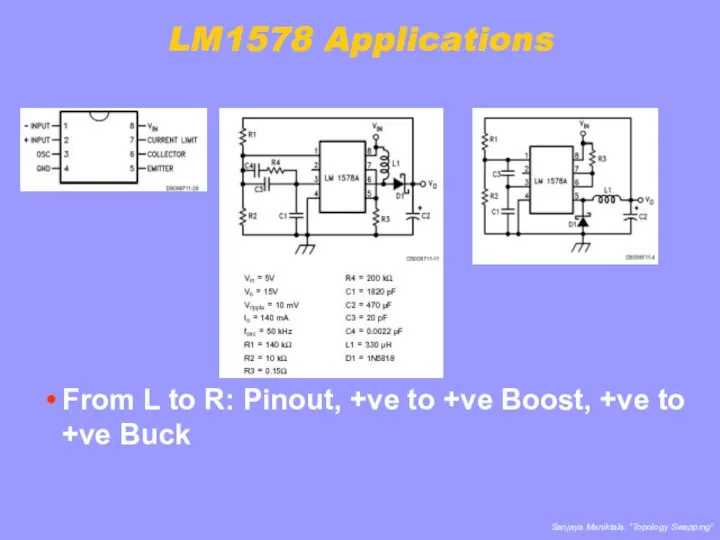
LM1578 Applications
From L to R: Pinout, +ve to +ve Boost, +ve
LM1578 Applications
From L to R: Pinout, +ve to +ve Boost, +ve
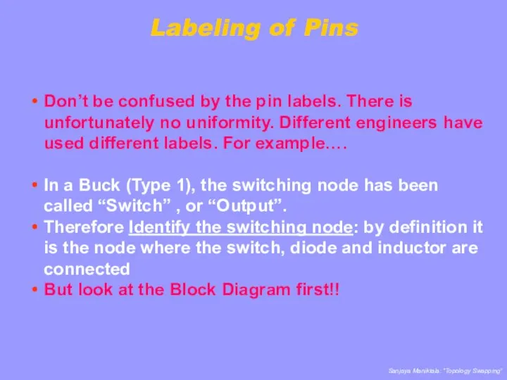
Labeling of Pins
Don’t be confused by the pin labels. There is
Labeling of Pins
Don’t be confused by the pin labels. There is
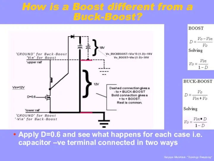
How is a Boost different from a Buck-Boost?
Apply D=0.6 and see
How is a Boost different from a Buck-Boost?
Apply D=0.6 and see
Boost and Buck-Boost compared
The main difference is in the feedback. Since
Boost and Buck-Boost compared
The main difference is in the feedback. Since
Nomenclature used
In this article we will use the word ‘Flyback’ to
Nomenclature used
In this article we will use the word ‘Flyback’ to
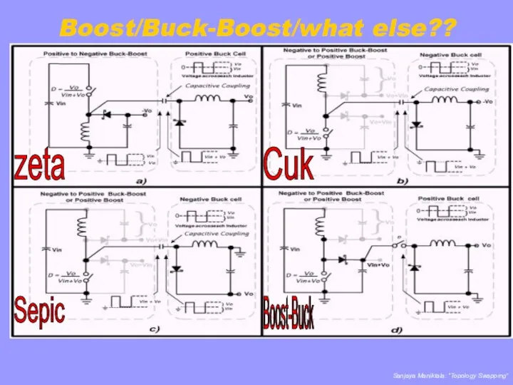
Boost/Buck-Boost/what else??
Boost/Buck-Boost/what else??
Now the crucial chain of logic behind hidden applications: the primary
Now the crucial chain of logic behind hidden applications: the primary
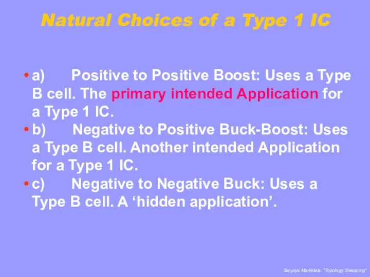
Natural Choices of a Type 1 IC
a) Positive to Positive Boost:
Natural Choices of a Type 1 IC
a) Positive to Positive Boost:
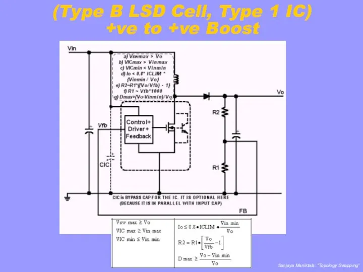
(Type B LSD Cell, Type 1 IC)
+ve to +ve Boost
(Type B LSD Cell, Type 1 IC)
+ve to +ve Boost
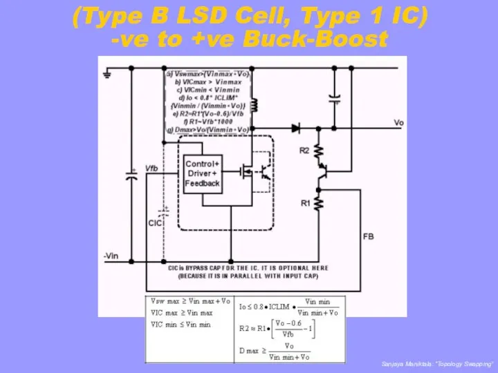
(Type B LSD Cell, Type 1 IC)
-ve to +ve Buck-Boost
(Type B LSD Cell, Type 1 IC)
-ve to +ve Buck-Boost
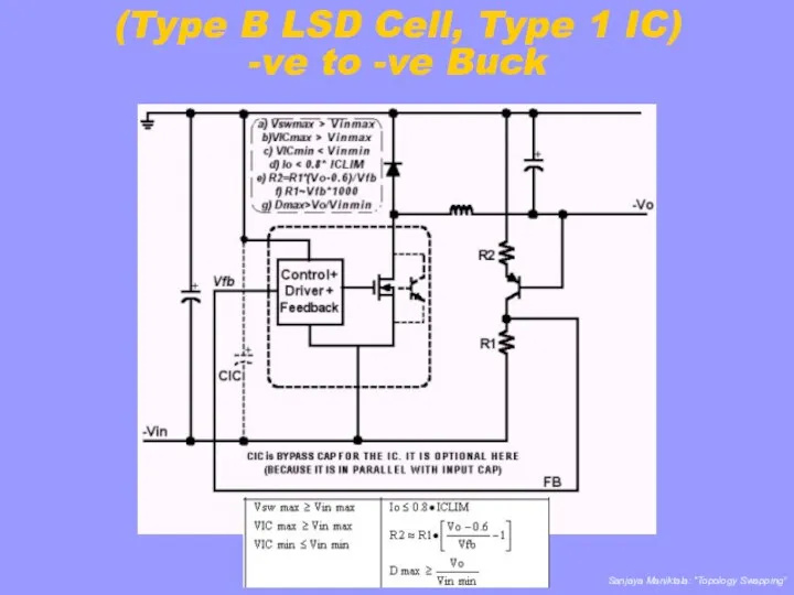
(Type B LSD Cell, Type 1 IC)
-ve to -ve Buck
(Type B LSD Cell, Type 1 IC)
-ve to -ve Buck
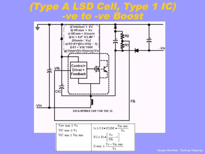
(Type A LSD Cell, Type 1 IC)
-ve to -ve Boost
(Type A LSD Cell, Type 1 IC)
-ve to -ve Boost
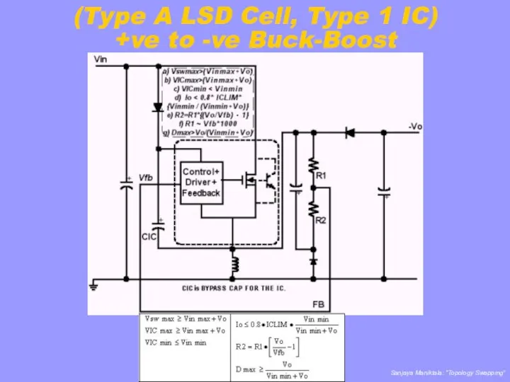
(Type A LSD Cell, Type 1 IC)
+ve to -ve Buck-Boost
(Type A LSD Cell, Type 1 IC)
+ve to -ve Buck-Boost
(Type A LSD Cell, Type 1 IC)
+ve to +ve Buck
(Type A LSD Cell, Type 1 IC)
+ve to +ve Buck
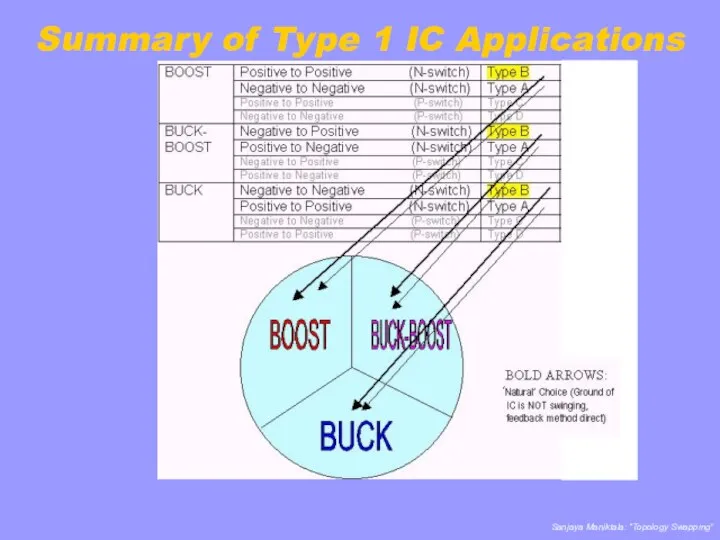
Summary of Type 1 IC Applications
Summary of Type 1 IC Applications
Natural Choices of a Type 2 IC
a) Positive to Positive Buck: Uses
Natural Choices of a Type 2 IC
a) Positive to Positive Buck: Uses
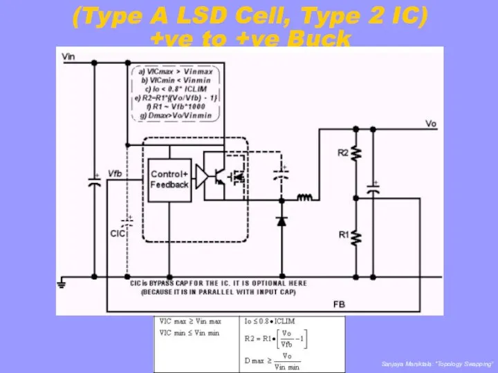
(Type A LSD Cell, Type 2 IC)
+ve to +ve Buck
(Type A LSD Cell, Type 2 IC)
+ve to +ve Buck
(Type A LSD Cell, Type 2 IC)
+ve to -ve Buck-Boost
(Type A LSD Cell, Type 2 IC)
+ve to -ve Buck-Boost
(Type A LSD Cell, Type 2 IC)
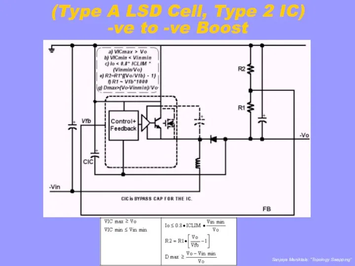
-ve to -ve Boost
(Type A LSD Cell, Type 2 IC)
-ve to -ve Boost
‘Forced’ Choices for Type 2 IC?
Because the Drain/Collector is NOT uncommitted,
‘Forced’ Choices for Type 2 IC?
Because the Drain/Collector is NOT uncommitted,
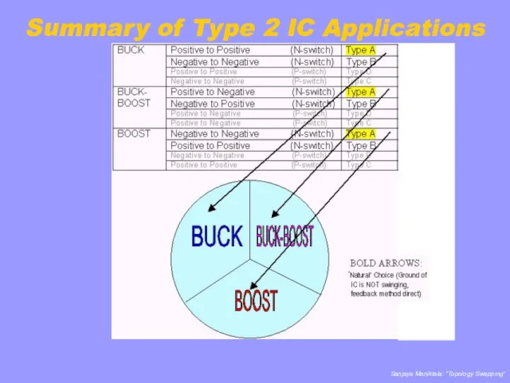
Summary of Type 2 IC Applications
Summary of Type 2 IC Applications
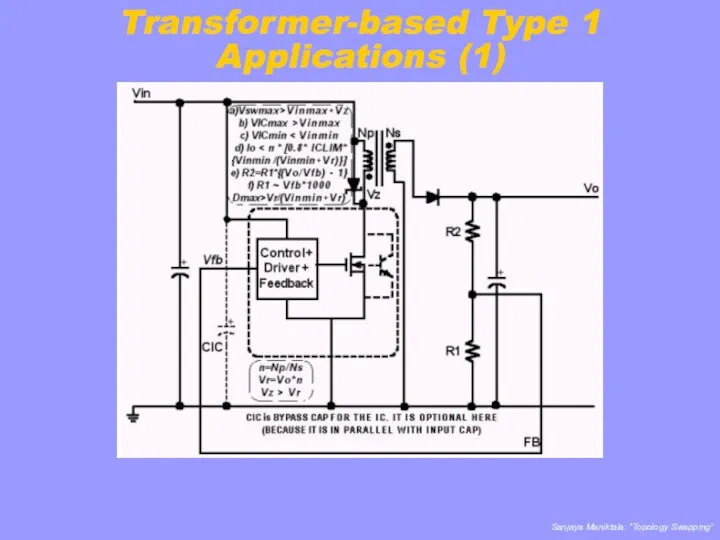
Transformer-based Type 1 Applications (1)
Transformer-based Type 1 Applications (1)
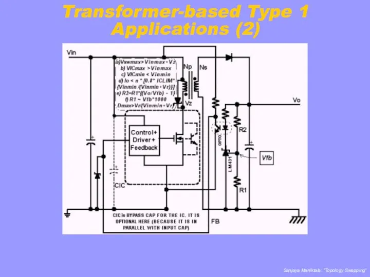
Transformer-based Type 1 Applications (2)
Transformer-based Type 1 Applications (2)
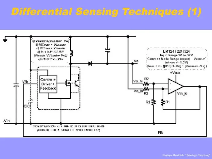
Differential Sensing Techniques (1)
Differential Sensing Techniques (1)
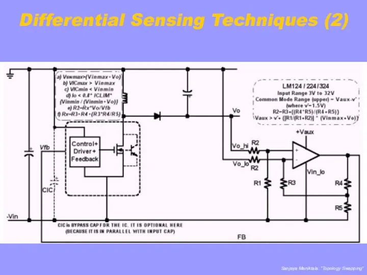
Differential Sensing Techniques (2)
Differential Sensing Techniques (2)
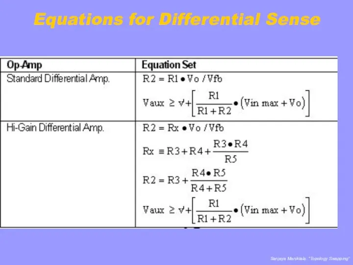
Equations for Differential Sense
Equations for Differential Sense
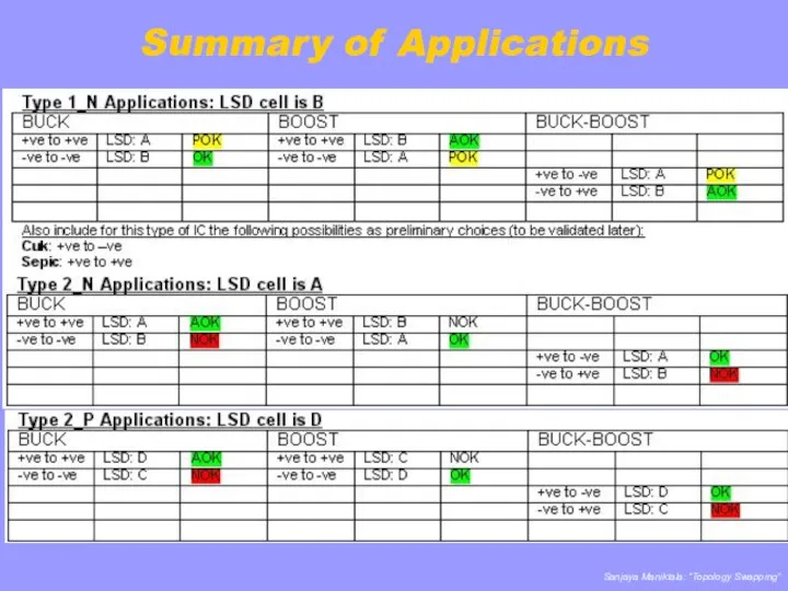
Summary of Applications
Summary of Applications
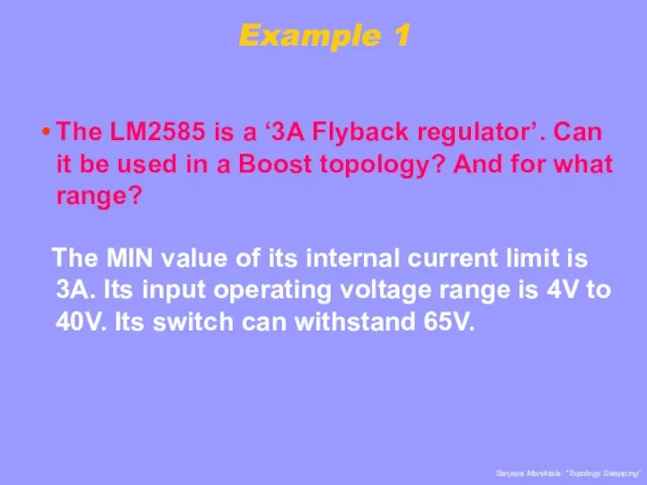
Example 1
The LM2585 is a ‘3A Flyback regulator’. Can it be
Example 1
The LM2585 is a ‘3A Flyback regulator’. Can it be
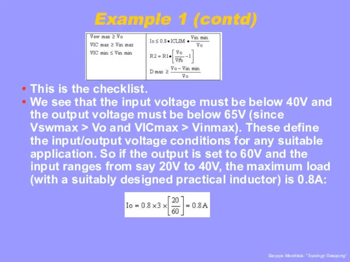
Example 1 (contd)
This is the checklist.
We see that the input voltage
Example 1 (contd)
This is the checklist.
We see that the input voltage
Example 2
The required application conditions are Vin ranging from 4.5V to
Example 2
The required application conditions are Vin ranging from 4.5V to
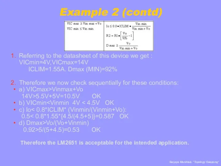
Example 2 (contd)
Referring to the datasheet of this device we get
Example 2 (contd)
Referring to the datasheet of this device we get
Nuances of Topology Swapping
One of the main concerns when we jump
Nuances of Topology Swapping
One of the main concerns when we jump
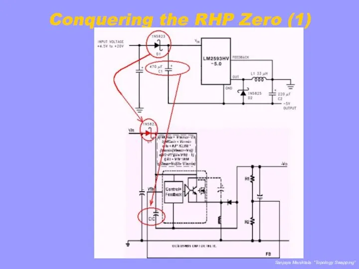
Conquering the RHP Zero (1)
Conquering the RHP Zero (1)
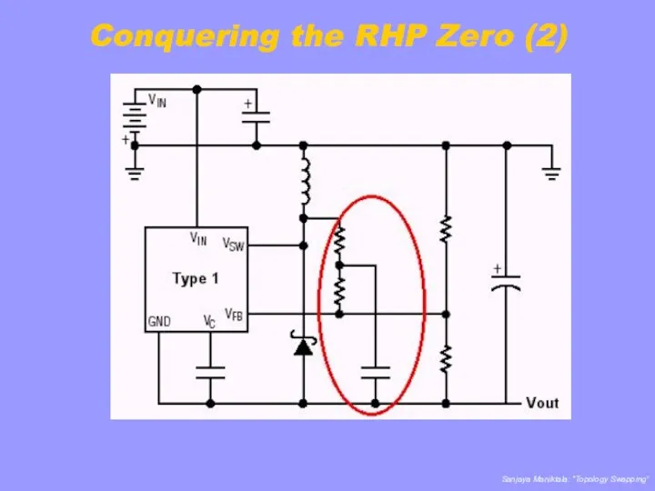
Conquering the RHP Zero (2)
Conquering the RHP Zero (2)
 Prezentatsia_Ryabov_N (2)
 Математика. Цели математики
 دليل خدمات قناة التكامل الحكومية
 Базы и базирование деталей. (Лекция 11)
 Автоматизація блоку осушення природного газу на автомобільній газонаповнювальній компресорній станції
 Методическая разработка. Дидактическое мультимедийное пособие Мир эмоций для детей старшего дошкольного возраста.
 Морфология и структурно-функциональная организация прокариот
 Договор банковского вклада
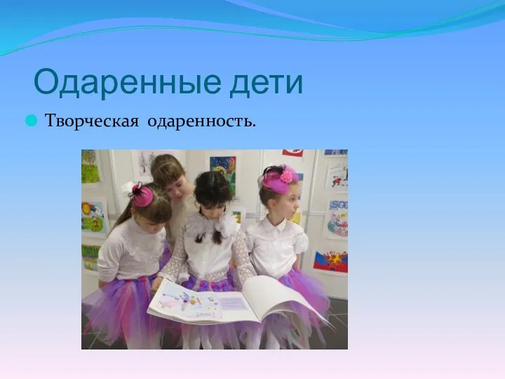 Одаренные дети . Творческая одаренность
 Эволюция жизни на Земле
 Духовно-нравственное воспитание младших школьников через изучение истории и культуры своей страны
 L_1_2_Sistema_Nats_bezopasn
 Арамсояу (лат. Cuscuta)
 Государство и экономика
 Вторая мировая: современные информационные возможности и организация проектной и исследовательской деятельности обучающихся
 Символизм. Первое течение модернизма, возникшее на русской почве
 Проект по благоустройству дворов жилых домов 9, 9А, 13, 15 на улице Молодёжной и проезда имени Заура Керейтова
 Протезирование дефектов зубов искусственными керамическими коронками
 Scanner & random
 Строим дом
 Кислотные обработки
 Виртуальная книжная выставка Сталинградская битва в лучших изданиях
 Образ Григория Мелехова (исследование по роману М. Шолохова Тихий Дон)
 Передача информации
 Атмосферное давление
 Неделя специальности Аналитический контроль качества химических соединений
 Использование вербально-коммуникативных методов в психолого-педагогических исследованиях
 Материал к уроку Безопасный интернет Диск