МЭМС и НЭМС: датчики ускорения и поворота, наноприводы, оптические и электронные системы презентация
- МЭМС и НЭМС: датчики ускорения и поворота, наноприводы, оптические и электронные системы

Содержание
- 2. Базовая структура датчика ускорения Base structure of acceleration sensor The basic structure of an accelerometer, consisting
- 3. Пьезорезистивный датчик ускорения Piezoresistive acceleration sensor Illustration of a piezoresistive accelerometer from Endevco Corp., fabricated using
- 4. Емкостной датчик Capacitive sensor Поперечная конфигурация Продольная конфигурация x0 Δx Δy ly
- 5. Емкостной датчик ускорения. Capacitive accelerometer. Illustration of a bulk micromachined capacitive accelerometer. The inertial mass in
- 6. Емкостной датчик ускорения – последовательность производства Production of capacitive accelerometer
- 7. Емкостной датчик ускорения. Capacitive accelerometer. Illustration of the basic structure of the ADXL family of surface
- 8. Емкостной датчик ускорения, произведенный с помощью DRIE. Capacitive accelerometer using DRIE. Scanning-electron micrograph of a DRIE
- 9. Сравнение пьезорезистивного, емкостного и электромагнитного методов измерения Comparison of different sensing
- 10. Элементы НЭМС NEMS elements Пассивные Passive Датчики Sensors Приводы (актуаторы) Actuators
- 11. Термический привод Thermal actuator if F is the external force
- 12. Пьезоэлектрический элемент (датчик или привод) Piezoelectric sensor and actuator An illustration of the piezoelectric effect on
- 13. Электростатический нанопривод Electrostatic actuator (a) An illustration of a parallel-plate electrostatic actuator with an applied voltage
- 14. Сравнение различных наноприводов Comparison of different nanoactuators
- 15. Гироскопы и датчики поворота Gyroscopes and tilt sensors
- 16. Кориолисово ускорение Coriolis acceleration Illustration of the Coriolis acceleration on an object moving with a velocity
- 17. Базовый датчик угловой скорости Base angular rate sensor Illustration of the tuning-fork structure for angular-rate sensing.
- 18. Датчик угловой скорости Angular-rate sensor Illustration of the angular-rate sensor from Daimler Benz. The structure is
- 19. Датчик угловой скорости Daimler Benz – последовательность производства Angular-rate sensor – fabrication steps
- 20. Датчик угловой скорости Angular-rate sensor Illustration of the Delphi Delco angular-rate sensor and the corresponding standing-wave
- 21. Датчик угловой скорости Angular-rate sensor Illustration of the CRS angular-rate sensor from Silicon Sensing Systems (UK&Jp)
- 22. Микро/наногенераторы: Vibration Harvesting Power vs. normalized frequency with varying electrical load resistance Illustration of unimorph configuration
- 23. Self-powered Wireless Corrosion-monitoring System Wireless sensor system schematics. The selfpowered sensor node transmits data to a
- 24. Оптические переключатели Optical switches Illustration of a 2 x 2 binary reflective optical switch fabricated using
- 25. Проекционные дисплеи Projectors Illustration of a single DMD pixel in its resting and actuated states. The
- 26. Микрозеркалa Micromirrors Illustration of optical beam steering using the switching of micromirrors. Off-axis illumination reflects into
- 27. Микрозеркало - последовательность производства Micromirror fabrication steps
- 28. Дифракционный оптический переключатель Optical diffraction switch Illustration of the operating principle of a single pixel in
- 29. Цветной проекционный элемент Color projection Implementation of color in a GLV pixel. The pitch of each
- 30. Перестраиваемый лазер Tunable laser Illustration of the building blocks of a laser. A gain medium amplifies
- 31. Внешний резонатор для перестраиваемого лазера External resonator for a tunable laser (a) Illustration of the Littman-Metcalf
- 32. Массив лазеров и оптоволокно Collimation of a laser from array into an optical fiber Schematic illustration
- 33. Микрозеркало Micromirror Schematic cross section of the micromirror used within the tunable laser from Santur Corporation.
- 34. Многоканальный оптический переключатель Multichannel optical switch Schematic illustration of the 3-D architecture for an N x
- 35. Замещение пассивных электронных элементов Replacement of passive electronic components
- 36. Индуктивность Microinductor The PARC inductor: (a) scanning-electron micrograph (SEM) of a five-turn solenoid inductor (the locations
- 37. Индуктивность - последовательность производства НЭМС Fabrication of microinductor
- 38. Переменная емкость Tunable capacitor
- 39. Резонатор Resonator Illustration of a micromachined folded-beam comb-drive resonator. The left comb drive actuates the device
- 40. Высокочастотный резонатор с термокомпенсацией Resonator with thermal compensation Illustration of the compensation scheme to reduce sensitivity
- 41. Переключатель Electric switch MicroAssembly Technologies of Richmond, California, USA Shock tolerance of 30,000G, insertion loss of
- 42. To be continued
- 44. Скачать презентацию
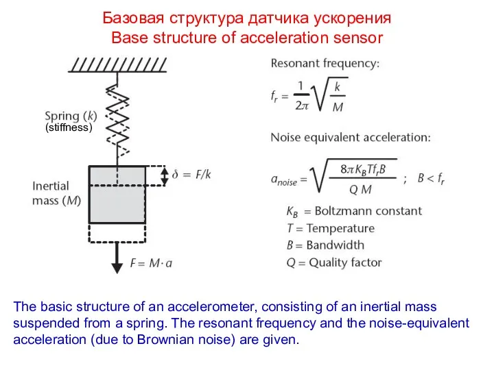
Базовая структура датчика ускорения
Base structure of acceleration sensor
The basic structure
Базовая структура датчика ускорения
Base structure of acceleration sensor
The basic structure
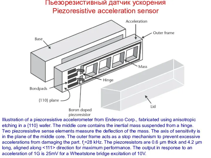
Пьезорезистивный датчик ускорения
Piezoresistive acceleration sensor
Illustration of a piezoresistive accelerometer from Endevco
Пьезорезистивный датчик ускорения
Piezoresistive acceleration sensor
Illustration of a piezoresistive accelerometer from Endevco
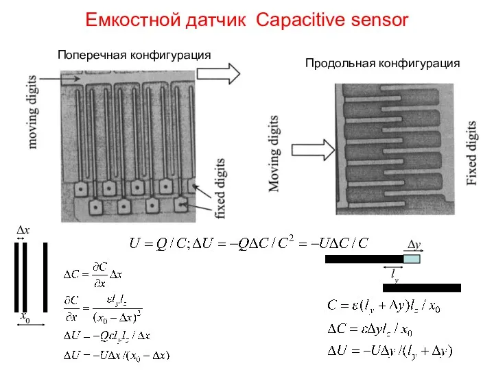
Емкостной датчик Capacitive sensor
Поперечная конфигурация
Продольная конфигурация
x0
Δx
Δy
ly
Емкостной датчик Capacitive sensor
Поперечная конфигурация
Продольная конфигурация
x0
Δx
Δy
ly
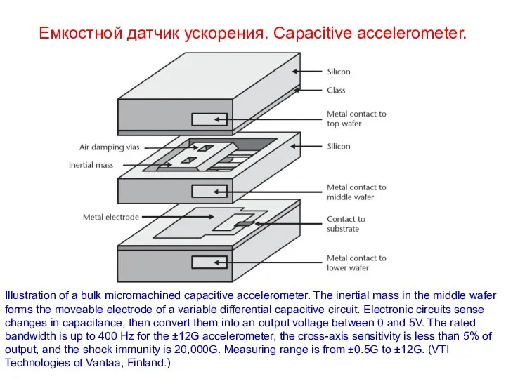
Емкостной датчик ускорения. Capacitive accelerometer.
Illustration of a bulk micromachined capacitive accelerometer.
Емкостной датчик ускорения. Capacitive accelerometer.
Illustration of a bulk micromachined capacitive accelerometer.
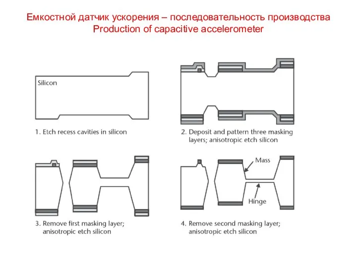
Емкостной датчик ускорения – последовательность производства
Production of capacitive accelerometer
Емкостной датчик ускорения – последовательность производства
Production of capacitive accelerometer
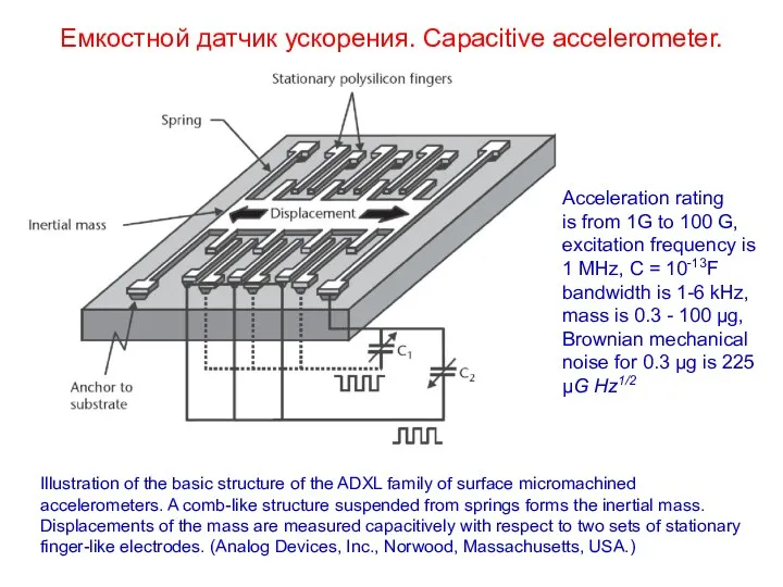
Емкостной датчик ускорения. Capacitive accelerometer.
Illustration of the basic structure of the
Емкостной датчик ускорения. Capacitive accelerometer.
Illustration of the basic structure of the
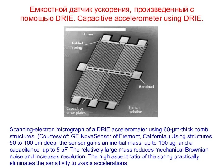
Емкостной датчик ускорения, произведенный с помощью DRIE. Capacitive accelerometer using DRIE.
Scanning-electron
Емкостной датчик ускорения, произведенный с помощью DRIE. Capacitive accelerometer using DRIE.
Scanning-electron
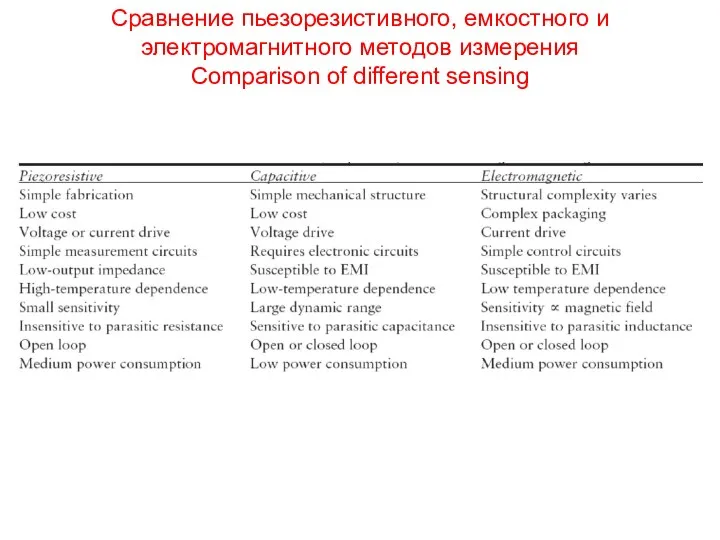
Сравнение пьезорезистивного, емкостного и электромагнитного методов измерения
Comparison of different sensing
Сравнение пьезорезистивного, емкостного и электромагнитного методов измерения
Comparison of different sensing
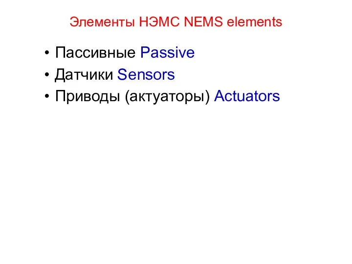
Элементы НЭМС NEMS elements
Пассивные Passive
Датчики Sensors
Приводы (актуаторы) Actuators
Элементы НЭМС NEMS elements
Пассивные Passive
Датчики Sensors
Приводы (актуаторы) Actuators
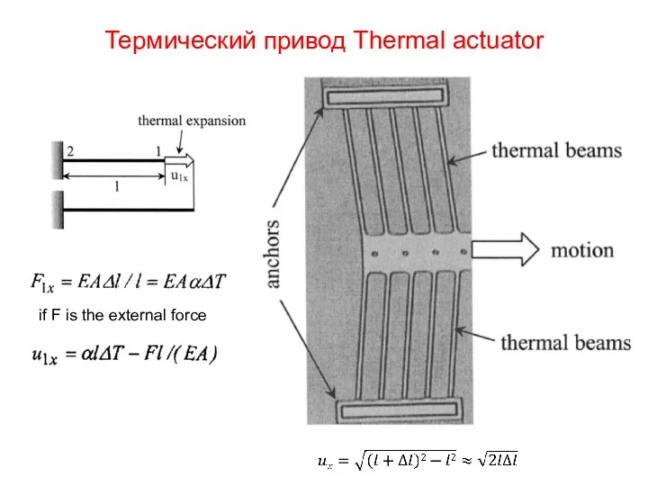
Термический привод Thermal actuator
if F is the external force
Термический привод Thermal actuator
if F is the external force
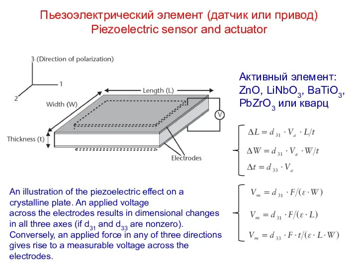
Пьезоэлектрический элемент (датчик или привод)
Piezoelectric sensor and actuator
An illustration of the
Пьезоэлектрический элемент (датчик или привод)
Piezoelectric sensor and actuator
An illustration of the
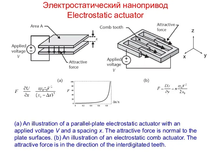
Электростатический нанопривод
Electrostatic actuator
(a) An illustration of a parallel-plate electrostatic actuator with
Электростатический нанопривод
Electrostatic actuator
(a) An illustration of a parallel-plate electrostatic actuator with
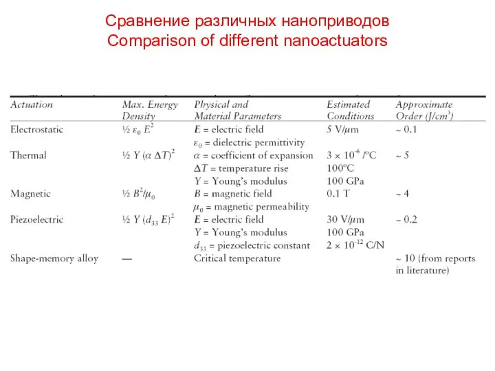
Сравнение различных наноприводов
Comparison of different nanoactuators
Сравнение различных наноприводов
Comparison of different nanoactuators
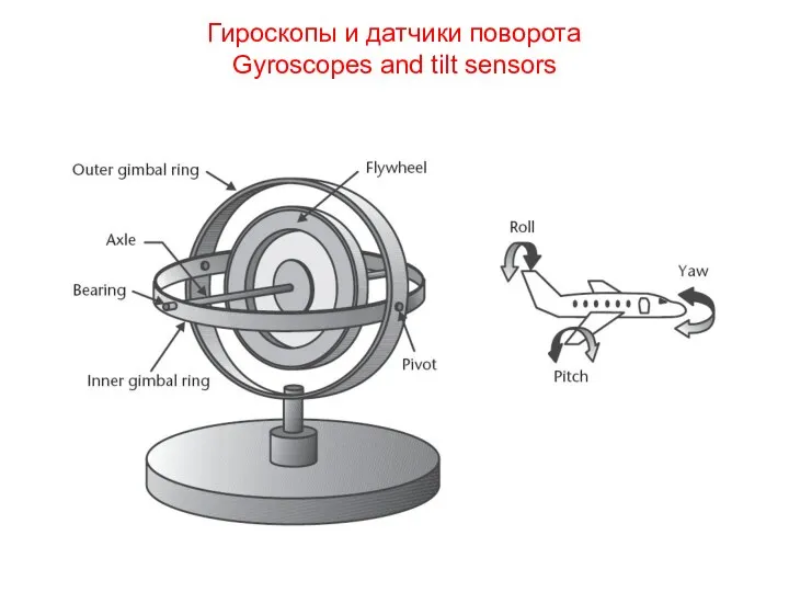
Гироскопы и датчики поворота
Gyroscopes and tilt sensors
Гироскопы и датчики поворота
Gyroscopes and tilt sensors
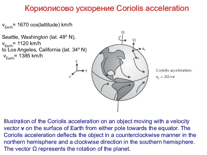
Кориолисово ускорение Coriolis acceleration
Illustration of the Coriolis acceleration on an object
Кориолисово ускорение Coriolis acceleration
Illustration of the Coriolis acceleration on an object
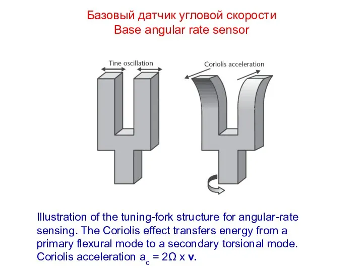
Базовый датчик угловой скорости
Base angular rate sensor
Illustration of the tuning-fork
Базовый датчик угловой скорости
Base angular rate sensor
Illustration of the tuning-fork
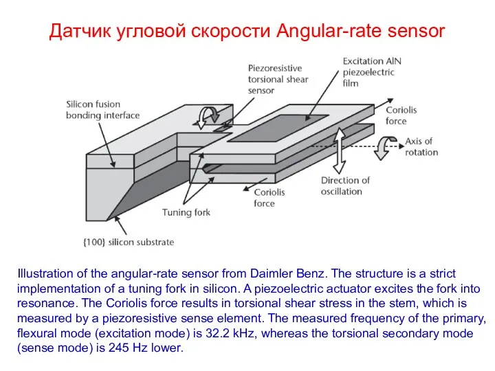
Датчик угловой скорости Angular-rate sensor
Illustration of the angular-rate sensor from
Датчик угловой скорости Angular-rate sensor
Illustration of the angular-rate sensor from
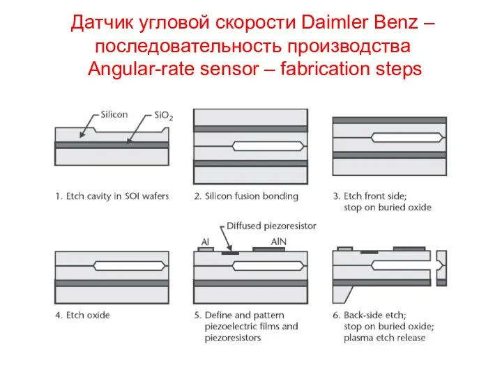
Датчик угловой скорости Daimler Benz – последовательность производства
Angular-rate sensor –
Датчик угловой скорости Daimler Benz – последовательность производства Angular-rate sensor –
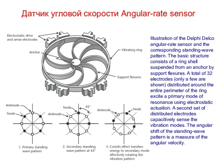
Датчик угловой скорости Angular-rate sensor
Illustration of the Delphi Delco angular-rate
Датчик угловой скорости Angular-rate sensor
Illustration of the Delphi Delco angular-rate
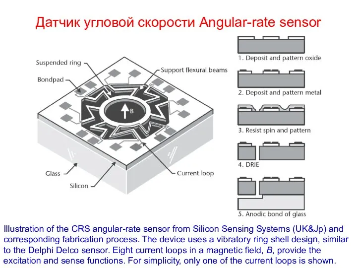
Датчик угловой скорости Angular-rate sensor
Illustration of the CRS angular-rate sensor
Датчик угловой скорости Angular-rate sensor
Illustration of the CRS angular-rate sensor
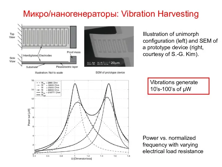
Микро/наногенераторы: Vibration Harvesting
Power vs. normalized frequency with varying electrical load resistance
Illustration
Микро/наногенераторы: Vibration Harvesting
Power vs. normalized frequency with varying electrical load resistance
Illustration
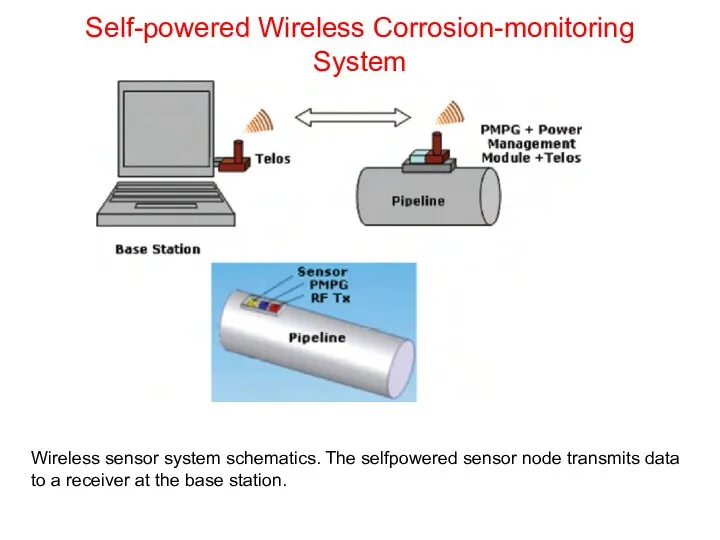
Self-powered Wireless Corrosion-monitoring System
Wireless sensor system schematics. The selfpowered sensor node
Self-powered Wireless Corrosion-monitoring System
Wireless sensor system schematics. The selfpowered sensor node
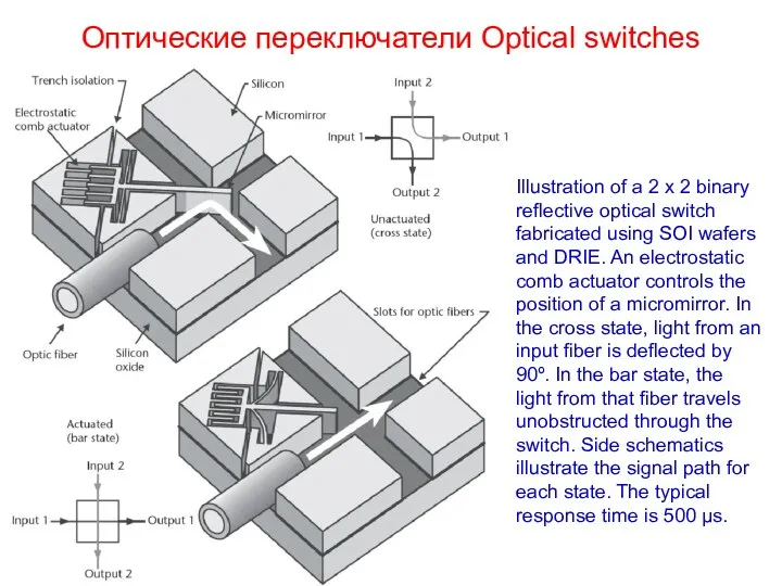
Оптические переключатели Optical switches
Illustration of a 2 x 2 binary reflective
Оптические переключатели Optical switches
Illustration of a 2 x 2 binary reflective
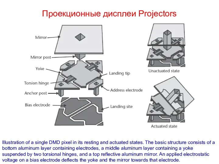
Проекционные дисплеи Projectors
Illustration of a single DMD pixel in its resting
Проекционные дисплеи Projectors
Illustration of a single DMD pixel in its resting
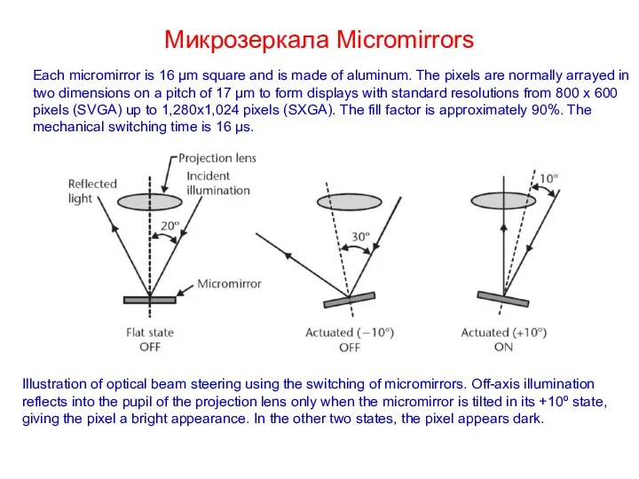
Микрозеркалa Micromirrors
Illustration of optical beam steering using the switching of micromirrors.
Микрозеркалa Micromirrors
Illustration of optical beam steering using the switching of micromirrors.
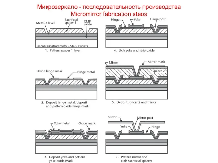
Микрозеркало - последовательность производства
Micromirror fabrication steps
Микрозеркало - последовательность производства
Micromirror fabrication steps
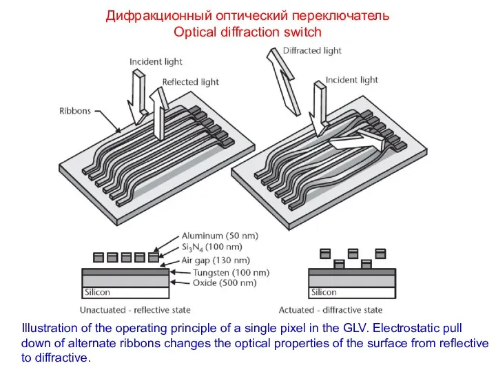
Дифракционный оптический переключатель
Optical diffraction switch
Illustration of the operating principle
Дифракционный оптический переключатель
Optical diffraction switch
Illustration of the operating principle
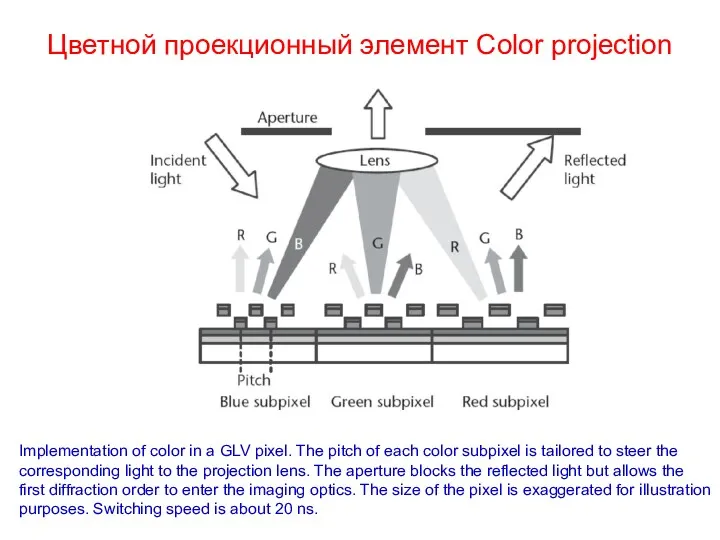
Цветной проекционный элемент Color projection
Implementation of color in a GLV pixel.
Цветной проекционный элемент Color projection
Implementation of color in a GLV pixel.
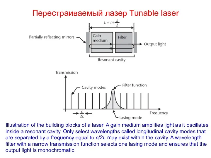
Перестраиваемый лазер Tunable laser
Illustration of the building blocks of a laser.
Перестраиваемый лазер Tunable laser
Illustration of the building blocks of a laser.
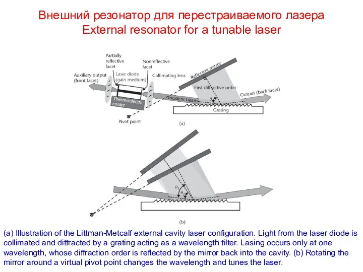
Внешний резонатор для перестраиваемого лазера External resonator for a tunable laser
(a)
Внешний резонатор для перестраиваемого лазера External resonator for a tunable laser
(a)
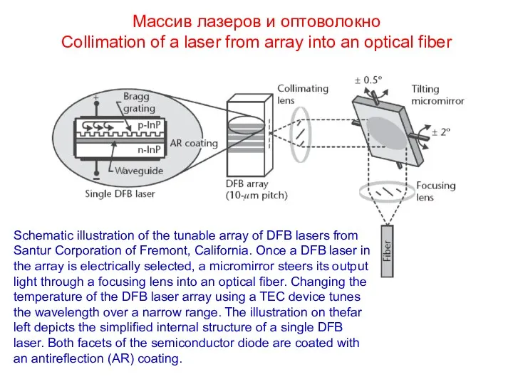
Массив лазеров и оптоволокно
Collimation of a laser from array into
Массив лазеров и оптоволокно Collimation of a laser from array into
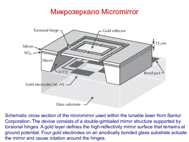
Микрозеркало Micromirror
Schematic cross section of the micromirror used within the tunable
Микрозеркало Micromirror
Schematic cross section of the micromirror used within the tunable
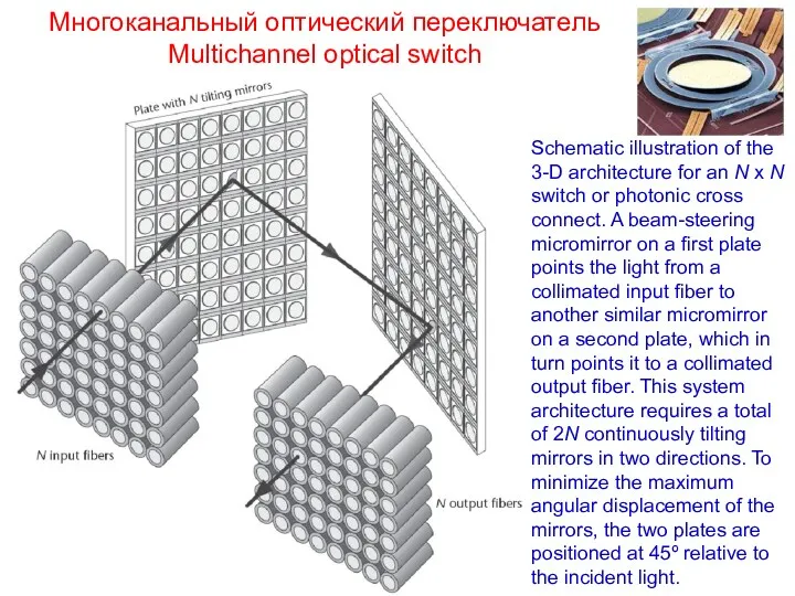
Многоканальный оптический переключатель
Multichannel optical switch
Schematic illustration of the 3-D architecture for
Многоканальный оптический переключатель
Multichannel optical switch
Schematic illustration of the 3-D architecture for
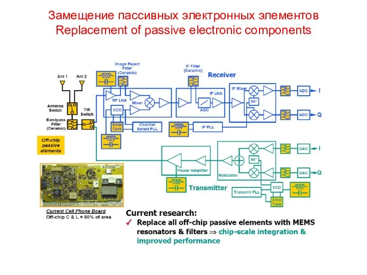
Замещение пассивных электронных элементов
Replacement of passive electronic components
Замещение пассивных электронных элементов
Replacement of passive electronic components
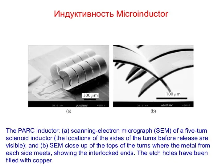
Индуктивность Microinductor
The PARC inductor: (a) scanning-electron micrograph (SEM) of a five-turn
Индуктивность Microinductor
The PARC inductor: (a) scanning-electron micrograph (SEM) of a five-turn
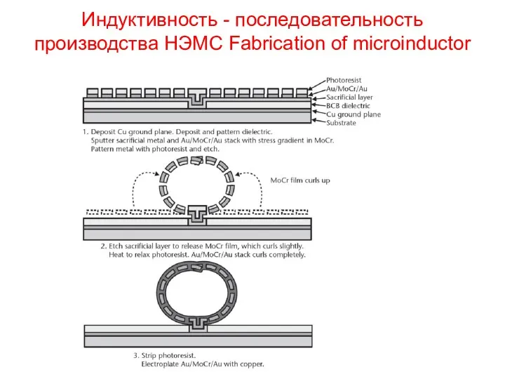
Индуктивность - последовательность производства НЭМС Fabrication of microinductor
Индуктивность - последовательность производства НЭМС Fabrication of microinductor
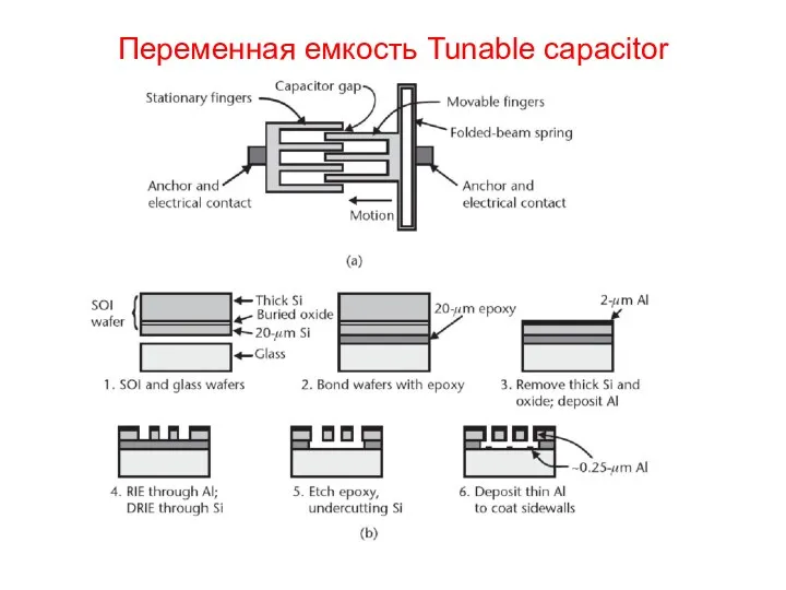
Переменная емкость Tunable capacitor
Переменная емкость Tunable capacitor
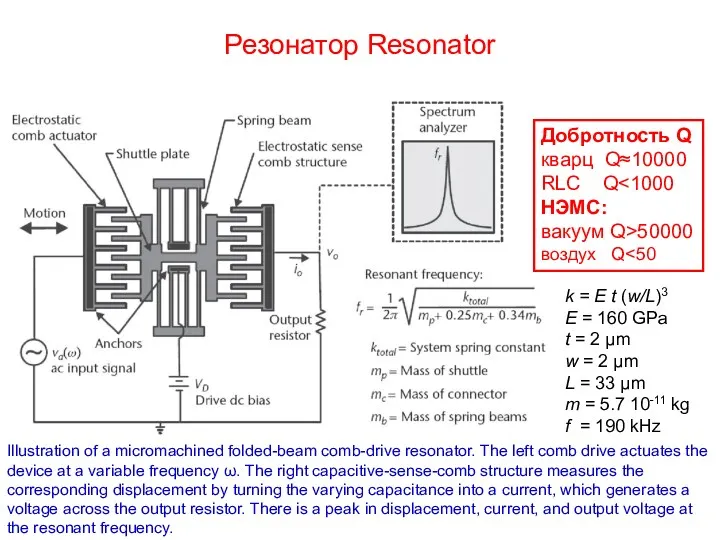
Резонатор Resonator
Illustration of a micromachined folded-beam comb-drive resonator. The left comb
Резонатор Resonator
Illustration of a micromachined folded-beam comb-drive resonator. The left comb
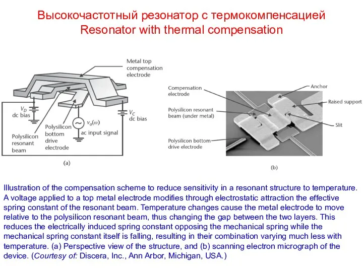
Высокочастотный резонатор с термокомпенсацией
Resonator with thermal compensation
Illustration of the compensation scheme
Высокочастотный резонатор с термокомпенсацией
Resonator with thermal compensation
Illustration of the compensation scheme
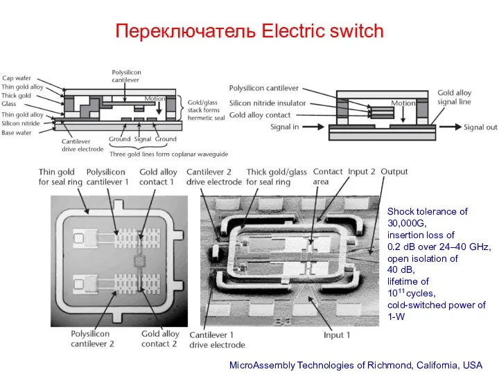
Переключатель Electric switch
MicroAssembly Technologies of Richmond, California, USA
Shock tolerance of
30,000G,
Переключатель Electric switch
MicroAssembly Technologies of Richmond, California, USA
Shock tolerance of 30,000G,

To be continued
To be continued
 Гидравлика
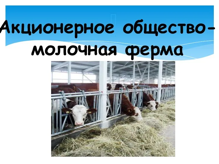 урок-игра по физике по теме Плотность
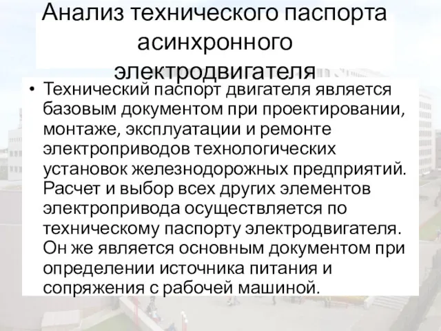 Анализ технического паспорта асинхронного электродвигателя
 Мегаконструкції. Найбільший в світі екскаватор
 Современные автомобили и двигатели
 Внедрение ФГОС общего образования второго поколения по физике
 Технология мини-исследования на уроках физики
 спектры
 Bbs wheels range 1999 ilustrated catalog
 Законам механики подчиняются движения всех окружающих нас тел
 Конкурс учителей Есть идея!
 Олимпийские игры и физика
 Памятка по неисправностям автосцепного устройства при техническом обслуживании
 Урок физики в 10 классе Газовые законы
 Звуковые волны
 Элементарные частицы. Микромир
 Идеальный газ. Основное уравнение МКТ идеального газа
 Нормирование точности поверхностей деталей машин по взаимному расположению, обозначения их на чертежах
 презентация по теме Сила трения.
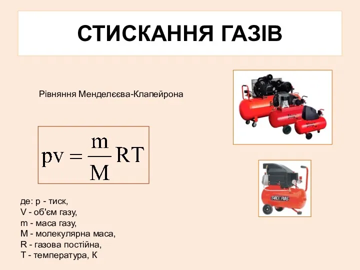 Стискання газів. Рівняння Менделєєва-Клапейрона
 Axles and shafts
 дополнение к уроку физики Испарение
 Изобретени радио А.С. Поповым
 Гармонические колебания и их характеристики
 Цепные передачи
 Mechanism
 Classical angular momentum and magnetic dipole moment
 Кинематика вращательного движения