- МЭМС и НЭМС: электронные системы, жидкостные вентили, насосы и биомедицинские системы

Содержание
- 2. Замещение пассивных электронных элементов Replacement of passive electronic components
- 3. Индуктивность Microinductor The PARC inductor: (a) scanning-electron micrograph (SEM) of a five-turn solenoid inductor (the locations
- 4. Индуктивность - последовательность производства НЭМС Fabrication of microinductor
- 5. Переменная емкость Tunable capacitor
- 6. Резонатор Resonator Illustration of a micromachined folded-beam comb-drive resonator. The left comb drive actuates the device
- 7. Высокочастотный резонатор с термокомпенсацией Resonator with thermal compensation Illustration of the compensation scheme to reduce sensitivity
- 8. Переключатель Electric switch MicroAssembly Technologies of Richmond, California, USA Shock tolerance of 30,000G, insertion loss of
- 9. Головка струйного принтера HP Head of HP inc-jet printer Heater temperature 250 °C, peak pressure 1.4
- 10. Головка струйного принтера HP - последовательность производства. Head of HP inc-jet printer - production steps
- 11. Головка струйного принтера HP Используется электронная кремниевая микросхема для упрощения управления головкой, удешевления и повышения надежности
- 12. .Регуляторы потоков. Microvalves • Electronic flow regulation of refrigerant for increased energy savings; • Electronically programmable
- 13. Нормально-открытый регулятор потока Normally open microvalve Illustration of a normally open valve from Redwood Microsystems, Ca.
- 14. Нормально-закрытый регулятор потока Normally closed microvalve Illustration of the basic operating mechanism of a normally closed
- 15. Ограничения регулятора потока с термо-пневматическим приводом Утечка тепла Leak of heat Скорость переключения Switching time Предельное
- 16. Микроклапан с приводом из металла с памятью формы Normally closed valve with shape-memory-alloy actuator Assembly of
- 17. Микроклапан – последовательность изготовления привода Normally closed valve with TiN actuator – production steps The valve
- 18. Микронасос Micropump Illustration of a cutout of a silicon micropump from the Fraunhofer Institute for Solid
- 19. Микронасос - последовательность производства НЭМС
- 20. Микрожидкостные системы Microfluidic systems
- 21. Смешивание в микроканалах Laminar flow and mixing Example of the use of laminar flow in microfluidics:
- 22. Смешивание в микроканалах Mixing in microchannels
- 23. Анализ ДНК - Lab on a Chip DNA analysis Schematic of the microfluidic device. The device
- 24. Анализ ДНК Two-spot system for interrogating DNA conformations after stretching in mixed microflows. (A) CAD drawing
- 25. Синтез ДНК DNA synthesis Twisted double-helix structure of DNA Polymerase chain reaction (PCR). Denaturing of the
- 26. Цепная реакция полимеразы в МЭМС Polymerase chain reaction in MEMS Illustrations of (a) the front side,
- 27. Электрофорезная сортировка ДНК Electrophoresis system for DNA separation Illustration of the fluid injection and separation steps
- 28. Микроэлектроды Microelectrode array Cross section of a microelectrode array showing two different metals for the electrodes
- 29. Анализ ДНК DNA analysis Illustration of the Nanogen electronic addressing and detection schemes. (a) A positive
- 30. Синтез массивов ДНК DNA synthesis With 25 nucleotides in a sequence, there are 425 (equal to
- 31. Анализ крови – экспресная диагностика рака Cancer tumor detection
- 32. Выращивание и изучение живых клеток Growth and study of living cells Photograph of a cultured syncytium
- 33. Интегрированная биосистема Integrated biosystem
- 34. Рынок НЭМС Analysis of Worldwide MEMS Markets (in Millions of U.S. Dollars) In-Stat/MDR, “Got MEMS? Industry
- 35. МЭМС и НЭМС представляют собой обширное семейство портативных приборов, датчиков и устройств. Wide variety of portable
- 37. Скачать презентацию
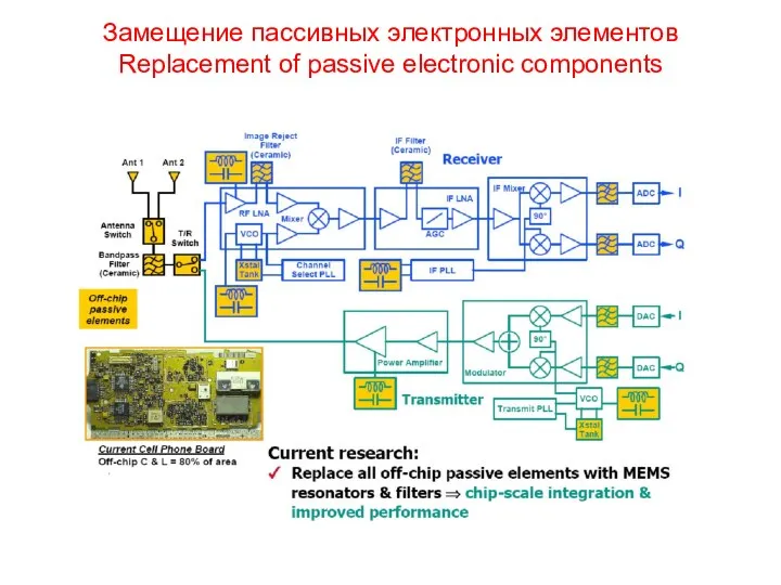
Замещение пассивных электронных элементов
Replacement of passive electronic components
Замещение пассивных электронных элементов
Replacement of passive electronic components
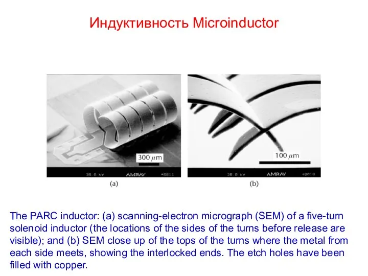
Индуктивность Microinductor
The PARC inductor: (a) scanning-electron micrograph (SEM) of a five-turn
Индуктивность Microinductor
The PARC inductor: (a) scanning-electron micrograph (SEM) of a five-turn
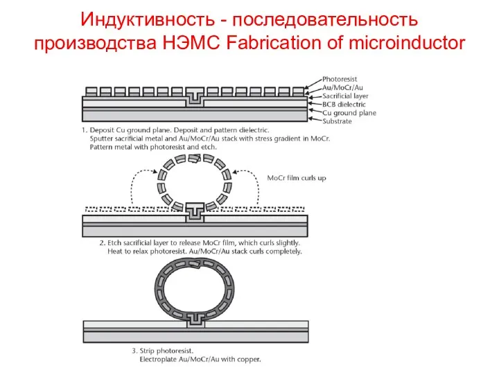
Индуктивность - последовательность производства НЭМС Fabrication of microinductor
Индуктивность - последовательность производства НЭМС Fabrication of microinductor
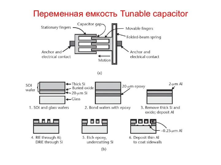
Переменная емкость Tunable capacitor
Переменная емкость Tunable capacitor
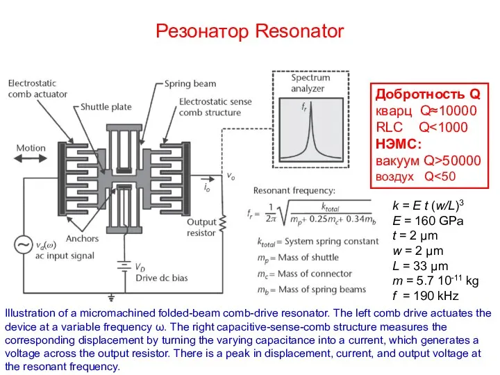
Резонатор Resonator
Illustration of a micromachined folded-beam comb-drive resonator. The left comb
Резонатор Resonator
Illustration of a micromachined folded-beam comb-drive resonator. The left comb
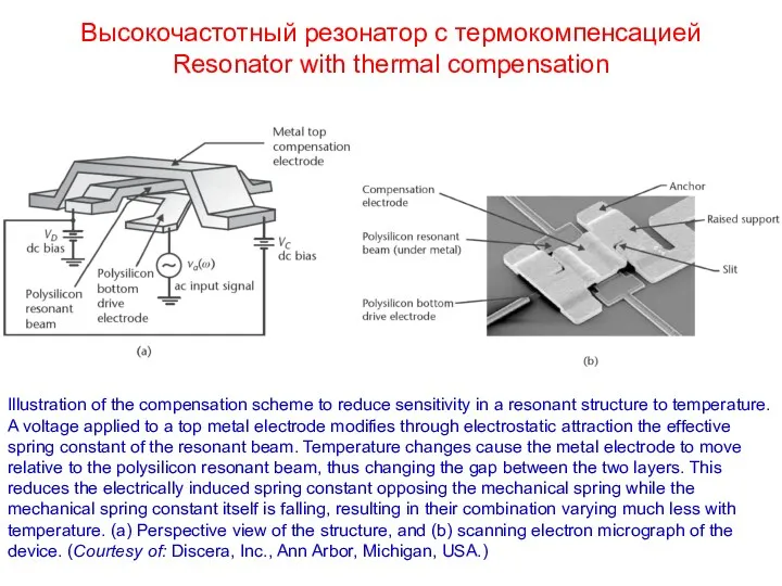
Высокочастотный резонатор с термокомпенсацией
Resonator with thermal compensation
Illustration of the compensation scheme
Высокочастотный резонатор с термокомпенсацией
Resonator with thermal compensation
Illustration of the compensation scheme
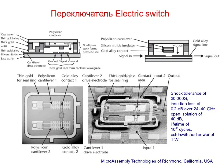
Переключатель Electric switch
MicroAssembly Technologies of Richmond, California, USA
Shock tolerance of
30,000G,
Переключатель Electric switch
MicroAssembly Technologies of Richmond, California, USA
Shock tolerance of 30,000G,
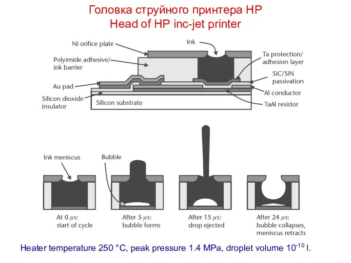
Головка струйного принтера HP
Head of HP inc-jet printer
Heater temperature 250 °C,
Головка струйного принтера HP
Head of HP inc-jet printer
Heater temperature 250 °C,
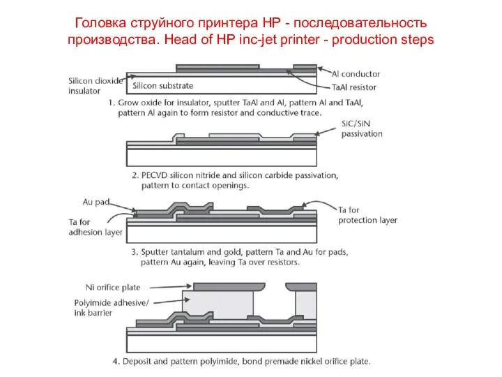
Головка струйного принтера HP - последовательность производства. Head of HP inc-jet
Головка струйного принтера HP - последовательность производства. Head of HP inc-jet
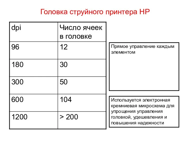
Головка струйного принтера HP
Используется электронная кремниевая микросхема для упрощения управления головкой,
Головка струйного принтера HP
Используется электронная кремниевая микросхема для упрощения управления головкой,
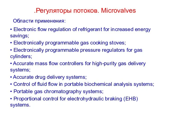
.Регуляторы потоков. Microvalves
• Electronic flow regulation of refrigerant for increased energy
.Регуляторы потоков. Microvalves
• Electronic flow regulation of refrigerant for increased energy
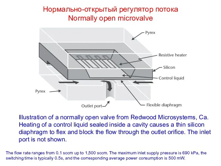
Нормально-открытый регулятор потока
Normally open microvalve
Illustration of a normally open valve
Нормально-открытый регулятор потока
Normally open microvalve
Illustration of a normally open valve
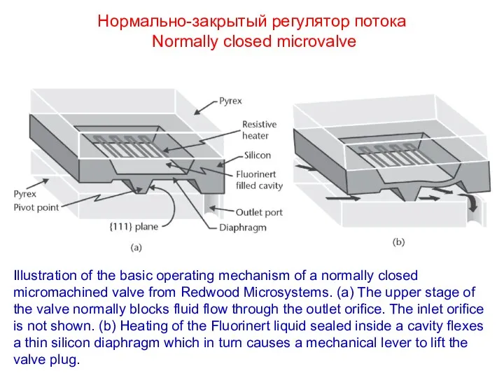
Нормально-закрытый регулятор потока
Normally closed microvalve
Illustration of the basic operating
Нормально-закрытый регулятор потока
Normally closed microvalve
Illustration of the basic operating
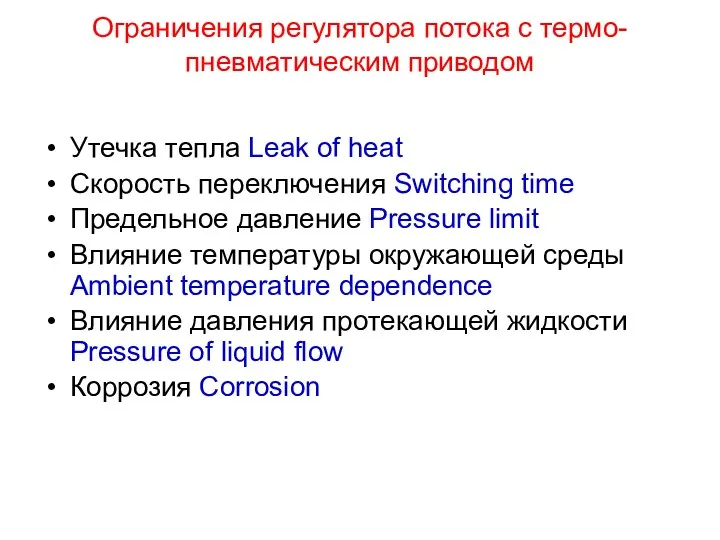
Ограничения регулятора потока с термо-пневматическим приводом
Утечка тепла Leak of heat
Скорость переключения
Ограничения регулятора потока с термо-пневматическим приводом
Утечка тепла Leak of heat
Скорость переключения
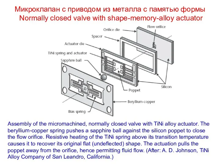
Микроклапан с приводом из металла с памятью формы
Normally closed valve
Микроклапан с приводом из металла с памятью формы Normally closed valve
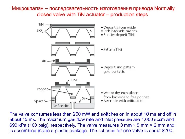
Микроклапан – последовательность изготовления привода Normally closed valve with TiN actuator
Микроклапан – последовательность изготовления привода Normally closed valve with TiN actuator
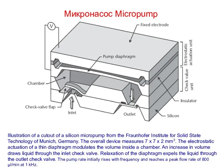
Микронасос Micropump
Illustration of a cutout of a silicon micropump from the
Микронасос Micropump
Illustration of a cutout of a silicon micropump from the
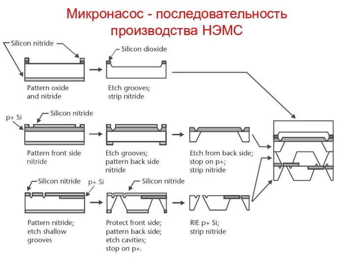
Микронасос - последовательность производства НЭМС
Микронасос - последовательность производства НЭМС
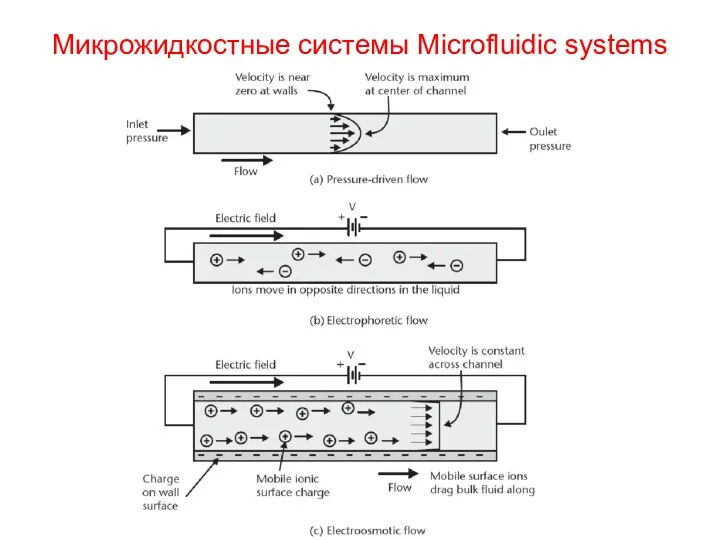
Микрожидкостные системы Microfluidic systems
Микрожидкостные системы Microfluidic systems
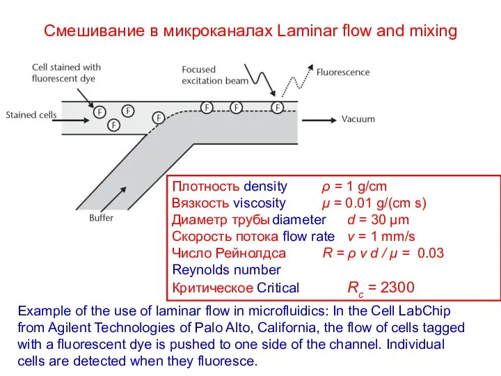
Смешивание в микроканалах Laminar flow and mixing
Example of the use of
Смешивание в микроканалах Laminar flow and mixing
Example of the use of
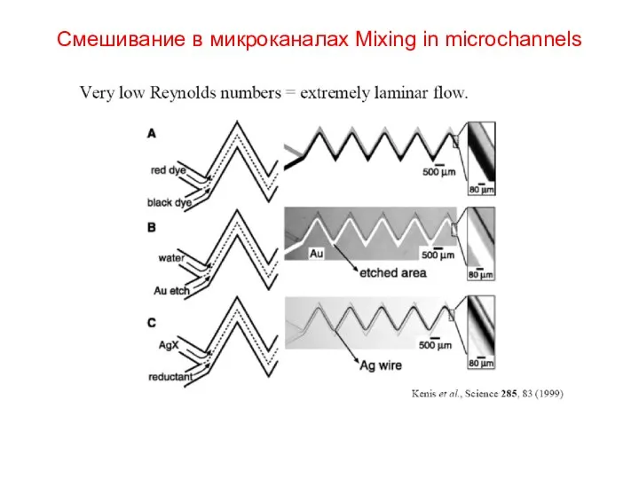
Смешивание в микроканалах Mixing in microchannels
Смешивание в микроканалах Mixing in microchannels
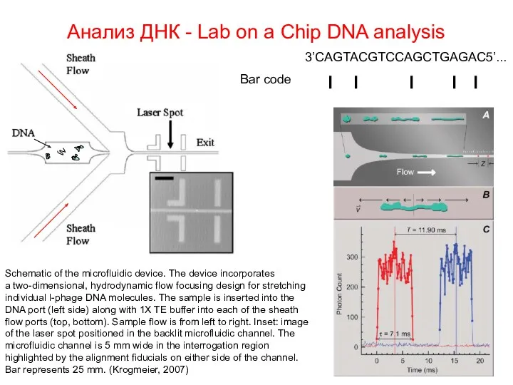
Анализ ДНК - Lab on a Chip DNA analysis
Schematic of the
Анализ ДНК - Lab on a Chip DNA analysis
Schematic of the
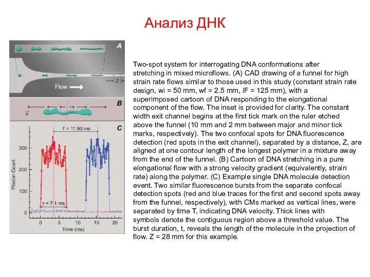
Анализ ДНК
Two-spot system for interrogating DNA conformations after
stretching in mixed microflows.
Анализ ДНК
Two-spot system for interrogating DNA conformations after
stretching in mixed microflows.
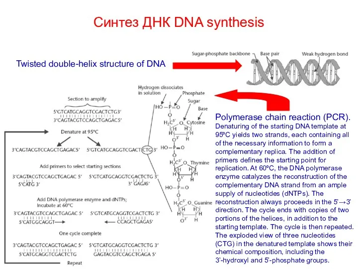
Синтез ДНК DNA synthesis
Twisted double-helix structure of DNA
Polymerase chain reaction (PCR).
Синтез ДНК DNA synthesis
Twisted double-helix structure of DNA
Polymerase chain reaction (PCR).
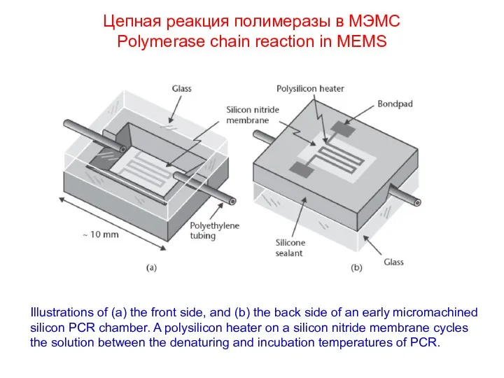
Цепная реакция полимеразы в МЭМС
Polymerase chain reaction in MEMS
Illustrations of (a)
Цепная реакция полимеразы в МЭМС
Polymerase chain reaction in MEMS
Illustrations of (a)
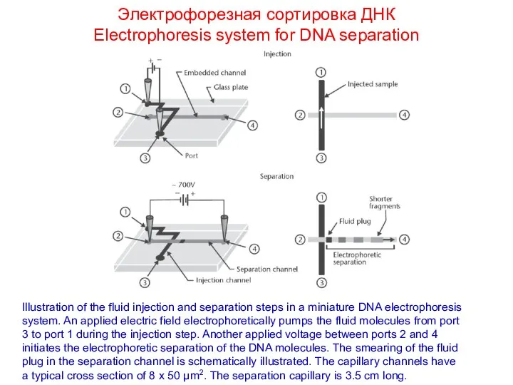
Электрофорезная сортировка ДНК
Electrophoresis system for DNA separation
Illustration of the fluid
Электрофорезная сортировка ДНК
Electrophoresis system for DNA separation
Illustration of the fluid
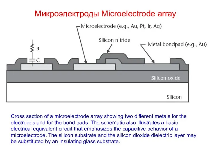
Микроэлектроды Microelectrode array
Cross section of a microelectrode array showing two
Микроэлектроды Microelectrode array
Cross section of a microelectrode array showing two
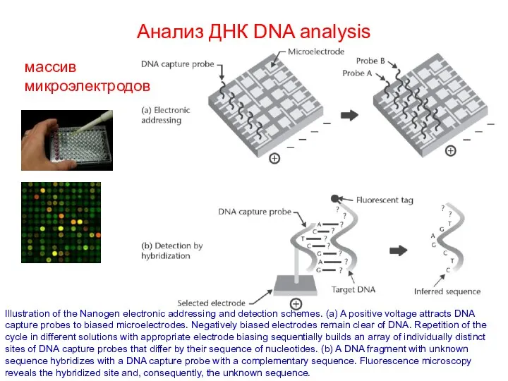
Анализ ДНК DNA analysis
Illustration of the Nanogen electronic addressing and detection
Анализ ДНК DNA analysis
Illustration of the Nanogen electronic addressing and detection
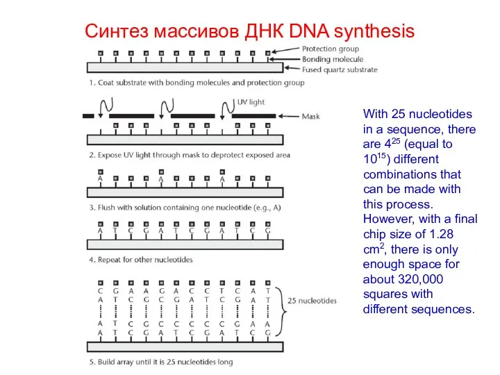
Синтез массивов ДНК DNA synthesis
With 25 nucleotides in a sequence, there
Синтез массивов ДНК DNA synthesis
With 25 nucleotides in a sequence, there
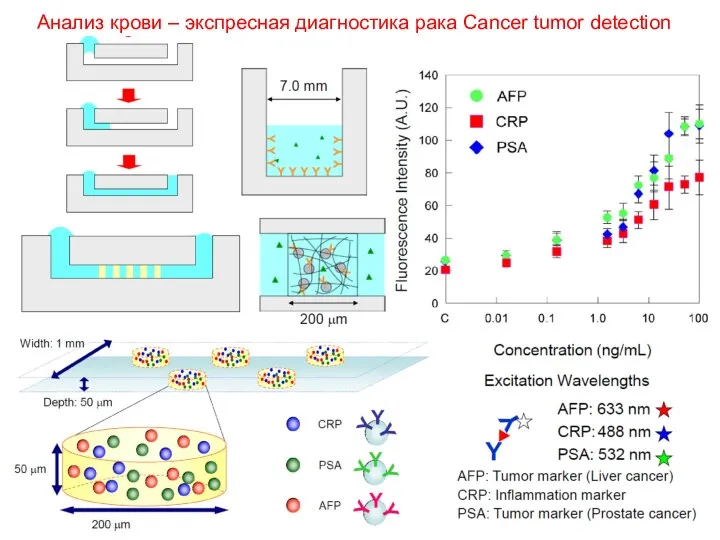
Анализ крови – экспресная диагностика рака Cancer tumor detection
Анализ крови – экспресная диагностика рака Cancer tumor detection
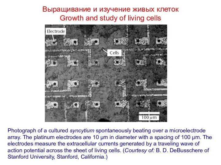
Выращивание и изучение живых клеток
Growth and study of living cells
Photograph
Выращивание и изучение живых клеток
Growth and study of living cells
Photograph
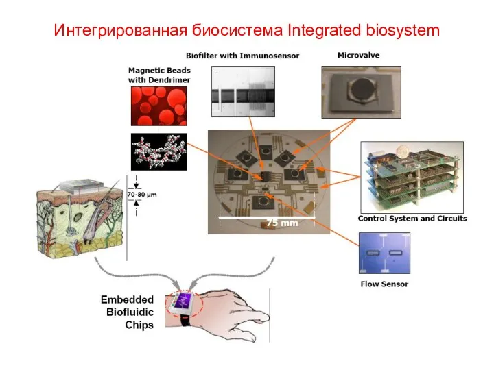
Интегрированная биосистема Integrated biosystem
Интегрированная биосистема Integrated biosystem
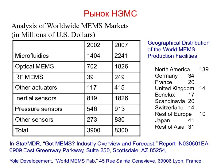
Рынок НЭМС
Analysis of Worldwide MEMS Markets
(in Millions of U.S. Dollars)
In-Stat/MDR,
Рынок НЭМС
Analysis of Worldwide MEMS Markets
(in Millions of U.S. Dollars)
In-Stat/MDR,
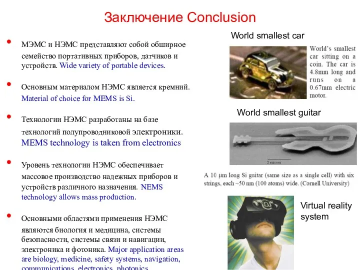
МЭМС и НЭМС представляют собой обширное семейство портативных приборов, датчиков и
МЭМС и НЭМС представляют собой обширное семейство портативных приборов, датчиков и
 Вільне падіння. Прискорення вільного падіння
 Классификация систем автоматического регулирования
 Снятие, замена приводного ремня ГРМ Chevrolet Lacetti
 Молекулярно-кинетические свойства коллоидных систем
 Презентация-игра, 7-8 класс
 Элементарные частицы
 История появления квадрокоптеров
 Делимость электрического заряда
 Урок по теме Электризация тел 8 класс
 Радиоактивность. Урок физики 9 класс
 Сила тока. Единицы силы тока
 Газораспределительный механизм
 Спидометр
 Kernfusion in der sonne
 Глава 5. Пьезоэлектрический эффект и электрострикция
 Агрегатные состояния вещества. Урок в 7 классе
 Презентация Способы изменения внутренней энергии 8 класс
 Элементы теории атомного ядра
 Шпонды және шлицты қосылыстар
 методическая разработка раздела курса физики 7 класса Давление
 Урок по теме Расчёт пути и времени движения 7 класс
 Акустика помещений
 Закон всемирного тяготения. Сила тяжести. Невесомость
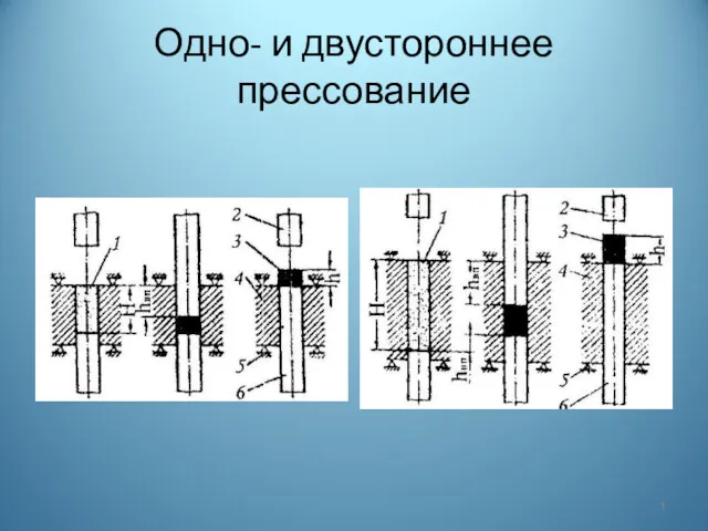 Одно- и двустороннее прессование деталей
 Количество теплоты. Единицы количества теплоты. Удельная теплоемкость. 8 класс
 сказка физического содержания Добро и зло
 Понятие о трехфазных цепях
 Основы генерирования и формирования сигналов. Лекция 2