- Solidification and crystalline imperfections (chapter 4)

Содержание
- 2. Solidification of Metals Metals are melted to produce finished and semi-finished parts. Two steps of solidification
- 3. Formation of Stable Nuclei Two main mechanisms: Homogenous and heterogeneous. Homogenous Nucleation : First and simplest
- 4. Energies involved in homogenous nucleation. Volume free energy Gv Released by liquid to solid transformation. ΔGv
- 5. Total Free Energy Total free energy is given by Nucleus Above critical radius r* Below critical
- 6. Critical Radius Versus Undercooling Greater the degree of undercooling, greater the change in volume free energy
- 7. Homogenous Nucleation Nucleation occurs in a liquid on the surfaces of structural material. Eg:- Insoluble impurities.
- 8. Growth of Crystals and Formation of Grain Structure Nucleus grow into crystals in different orientations. Crystal
- 9. Types of Grains Equiaxed Grains: Crystals, smaller in size, grow equally in all directions. Formed at
- 10. Casting in Industries In industries, molten metal is cast into either semi finished or finished parts.
- 11. Iron Smelting: Video Please click on the following figure to open the video. (This video has
- 12. Grain Structure in Industrial castings To produce cast ingots with fine grain size, grain refiners are
- 13. Solidification of Single Crystal For some applications (Eg: Gas turbine blades-high temperature environment), single crystals are
- 14. Czochralski Process This method is used to produce single crystal of silicon for electronic wafers. A
- 15. Metallic Solid Solutions Alloys are used in most engineering applications. Alloy is an mixture of two
- 16. Substitutional Solid Solution Solute atoms substitute for parent solvent atom in a crystal lattice. The structure
- 17. Substitutional Solid Solution (Cont..) The solubility of solids is greater if The diameter of atoms not
- 18. Interstitial Solid Solution Solute atoms fit in between the voids (interstices) of solvent atoms. Solvent atoms
- 19. Crystalline Imperfections No crystal is perfect. Imperfections affect mechanical properties, chemical properties and electrical properties. Imperfections
- 20. Point Defects – Vacancy Vacancy is formed due to a missing atom. Vacancy is formed (one
- 21. Point Defects - Interstitially Atom in a crystal, sometimes, occupies interstitial site. This does not occur
- 22. Point Defects in Ionic Crystals Complex as electric neutrality has to be maintained. If two appositely
- 23. Line Defects – (Dislocations) Lattice distortions are centered around a line. Formed during Solidification Permanent Deformation
- 24. Edge Dislocation Created by insertion of extra half planes of atoms. Positive edge dislocation Negative edge
- 25. Screw Dislocation Created due to shear stresses applied to regions of a perfect crystal separated by
- 26. Mixed Dislocation Most crystal have components of both edge and screw dislocation. Dislocation, since have irregular
- 27. Planar Defects Grain boundaries, twins, low/high angle boundaries, twists and stacking faults Free surface is also
- 28. Grain Boundaries Grain boundaries separate grains. Formed due to simultaneously growing crystals meeting each other. Width
- 29. Twin Boundaries Twin: A region in which mirror image pf structure exists across a boundary. Formed
- 30. Other Planar Defects Small angle tilt boundary: Array of edge dislocations tilts two regions of a
- 31. Observing Grain Boundaries - Metallography To observe grain boundaries, the metal sample must be first mounted
- 32. Virtual Lab Modules Click on the following figures to open the virtual lab modules related to
- 33. Effect of Etching Unetched Steel 200 X Etched Steel 200 X Unetched Brass 200 X Etched
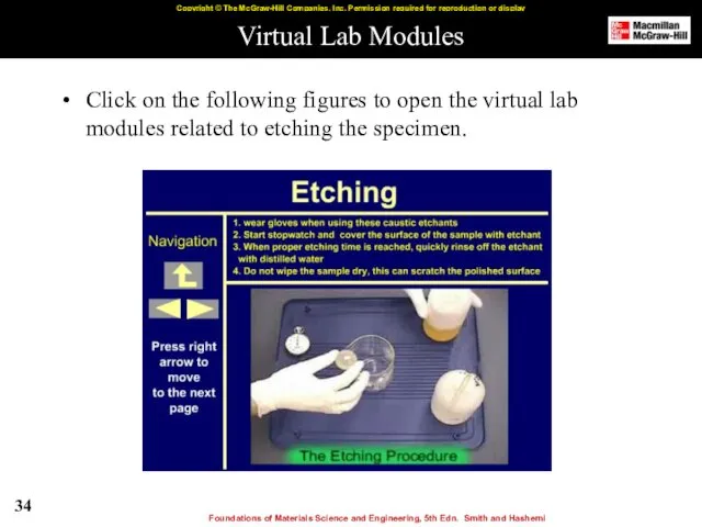
- 34. Virtual Lab Modules Click on the following figures to open the virtual lab modules related to
- 35. Virtual Lab Modules Click on the following figures to open the virtual lab modules related to
- 36. Grain Size Affects the mechanical properties of the material The smaller the grain size, more are
- 37. Measuring Grain Size ASTM grain size number ‘n’ is a measure of grain size. N =
- 38. Measuring ASTM Grain Size Number Click the Image below to play the tutorial.
- 39. Average Grain Diameter Average grain diameter more directly represents grain size. Random line of known length
- 40. Virtual Lab Module Click on the following figures to open the virtual lab modules related to
- 41. Transmission Electron Microscope Electron produced by heated tungsten filament. Accelerated by high voltage (75 - 120
- 42. TEM (..Cont) TEM needs complex sample preparation Very thin specimen needed ( several hundred nanometers) High
- 43. The Scanning Electron Microscope Electron source generates electrons. Electrons hit the surface and secondary electrons are
- 44. Scanning Probe Microscopy Scanning Tunneling Microscope (STM) and Atomic Force Microscope (AFM). Sub-nanometer magnification. Atomic scale
- 45. Scanning Tunneling Microscope Tip placed one atom diameter from surface. Voltage applied across tip and surface.
- 47. Скачать презентацию
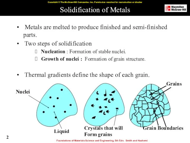
Solidification of Metals
Metals are melted to produce finished and semi-finished
Solidification of Metals
Metals are melted to produce finished and semi-finished
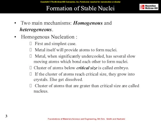
Formation of Stable Nuclei
Two main mechanisms: Homogenous and heterogeneous.
Homogenous
Formation of Stable Nuclei
Two main mechanisms: Homogenous and heterogeneous.
Homogenous
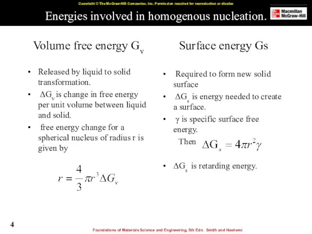
Energies involved in homogenous nucleation.
Volume free energy Gv
Released by liquid
Energies involved in homogenous nucleation.
Volume free energy Gv
Released by liquid
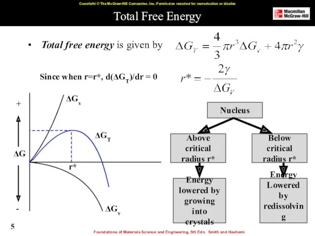
Total Free Energy
Total free energy is given by
Nucleus
Above critical
radius r*
Below
Total Free Energy
Total free energy is given by
Nucleus
Above critical
radius r*
Below
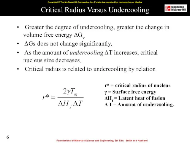
Critical Radius Versus Undercooling
Greater the degree of undercooling, greater the
Critical Radius Versus Undercooling
Greater the degree of undercooling, greater the
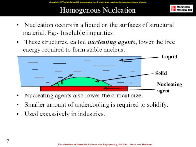
Homogenous Nucleation
Nucleation occurs in a liquid on the surfaces of
Homogenous Nucleation
Nucleation occurs in a liquid on the surfaces of
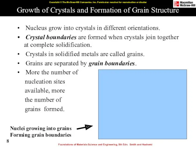
Growth of Crystals and Formation of Grain Structure
Nucleus grow into
Growth of Crystals and Formation of Grain Structure
Nucleus grow into
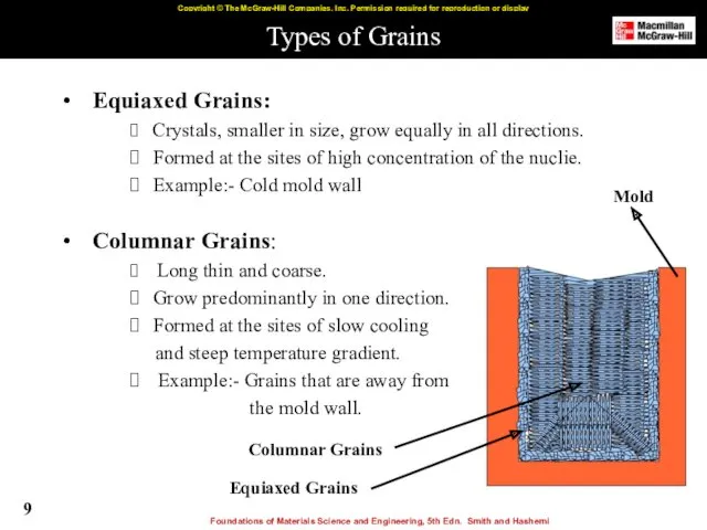
Types of Grains
Equiaxed Grains:
Crystals, smaller in size, grow
Types of Grains
Equiaxed Grains:
Crystals, smaller in size, grow
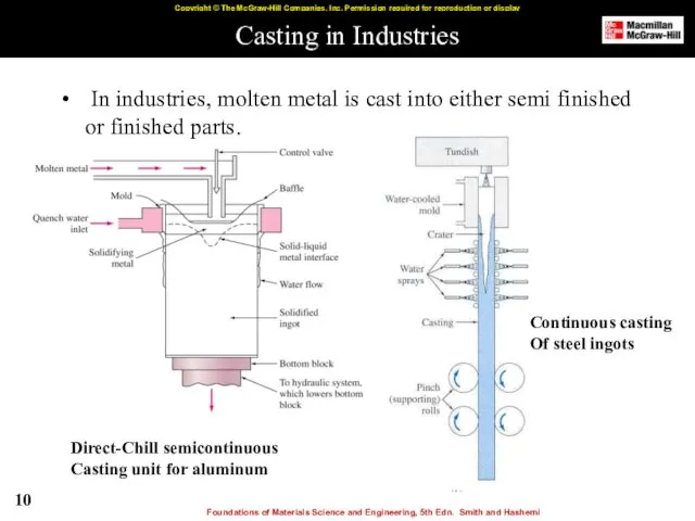
Casting in Industries
In industries, molten metal is cast into either
Casting in Industries
In industries, molten metal is cast into either
Iron Smelting: Video
Please click on the following figure to open
Iron Smelting: Video
Please click on the following figure to open
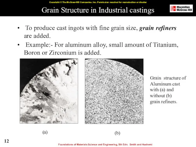
Grain Structure in Industrial castings
To produce cast ingots with fine
Grain Structure in Industrial castings
To produce cast ingots with fine
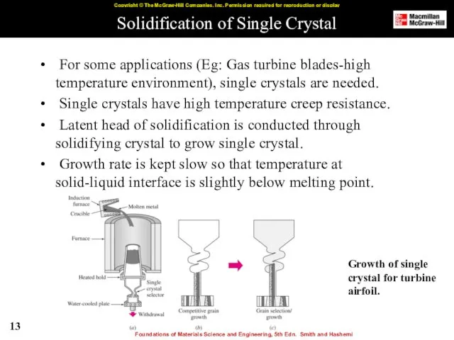
Solidification of Single Crystal
For some applications (Eg: Gas turbine blades-high
Solidification of Single Crystal
For some applications (Eg: Gas turbine blades-high
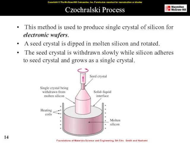
Czochralski Process
This method is used to produce single crystal of
Czochralski Process
This method is used to produce single crystal of
Metallic Solid Solutions
Alloys are used in most engineering applications.
Alloy
Metallic Solid Solutions
Alloys are used in most engineering applications.
Alloy
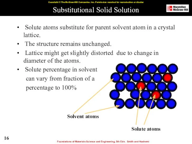
Substitutional Solid Solution
Solute atoms substitute for parent solvent atom
Substitutional Solid Solution
Solute atoms substitute for parent solvent atom
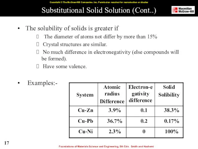
Substitutional Solid Solution (Cont..)
The solubility of solids is greater if
Substitutional Solid Solution (Cont..)
The solubility of solids is greater if
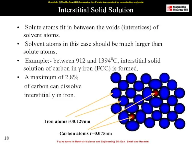
Interstitial Solid Solution
Solute atoms fit in between the voids
Interstitial Solid Solution
Solute atoms fit in between the voids
Crystalline Imperfections
No crystal is perfect.
Imperfections affect mechanical properties, chemical
Crystalline Imperfections
No crystal is perfect.
Imperfections affect mechanical properties, chemical
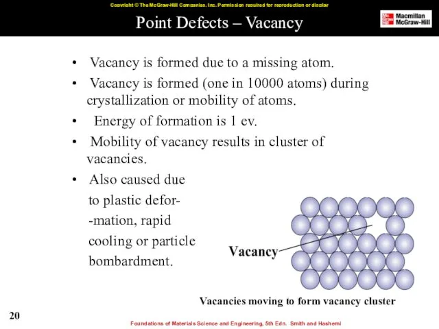
Point Defects – Vacancy
Vacancy is formed due to a
Point Defects – Vacancy
Vacancy is formed due to a
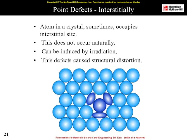
Point Defects - Interstitially
Atom in a crystal, sometimes, occupies interstitial site.
Point Defects - Interstitially
Atom in a crystal, sometimes, occupies interstitial site.
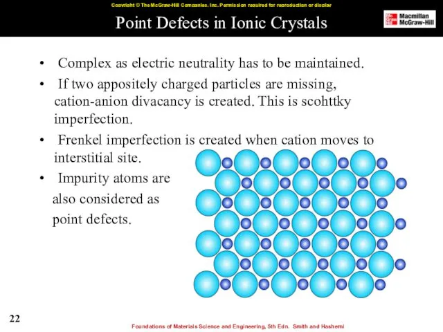
Point Defects in Ionic Crystals
Complex as electric neutrality has to
Point Defects in Ionic Crystals
Complex as electric neutrality has to
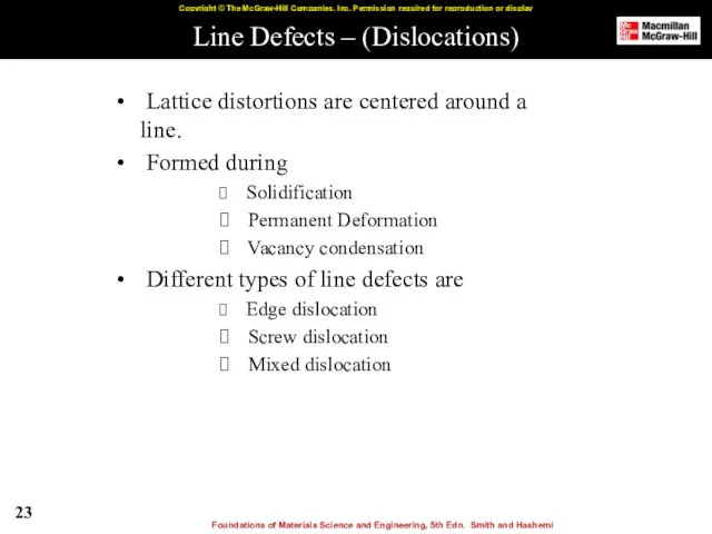
Line Defects – (Dislocations)
Lattice distortions are centered around a
Line Defects – (Dislocations)
Lattice distortions are centered around a
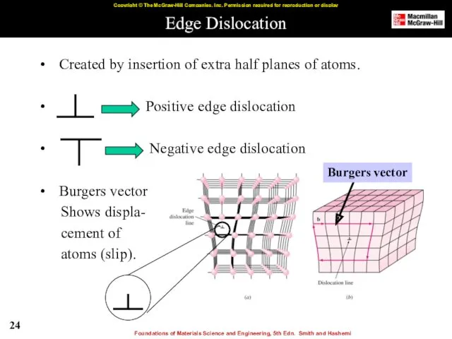
Edge Dislocation
Created by insertion of extra half planes of
Edge Dislocation
Created by insertion of extra half planes of
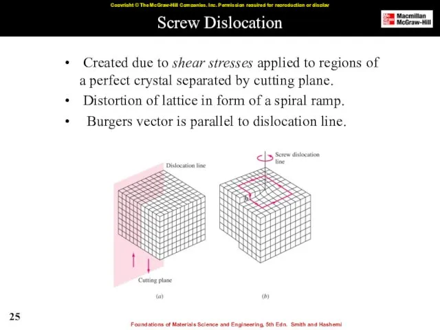
Screw Dislocation
Created due to shear stresses applied to regions of
Screw Dislocation
Created due to shear stresses applied to regions of
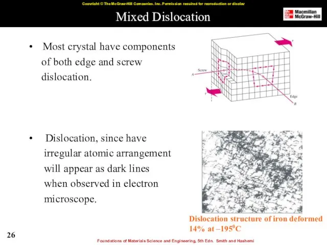
Mixed Dislocation
Most crystal have components
of both edge and
Mixed Dislocation
Most crystal have components
of both edge and
Planar Defects
Grain boundaries, twins, low/high angle boundaries, twists and stacking faults
Planar Defects
Grain boundaries, twins, low/high angle boundaries, twists and stacking faults
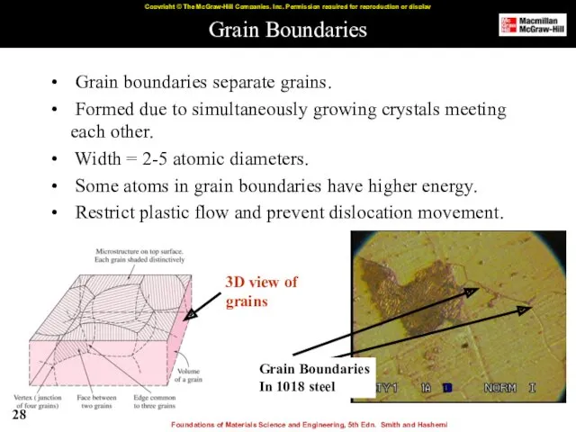
Grain Boundaries
Grain boundaries separate grains.
Formed due to simultaneously growing
Grain Boundaries
Grain boundaries separate grains.
Formed due to simultaneously growing
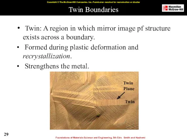
Twin Boundaries
Twin: A region in which mirror image pf structure
Twin Boundaries
Twin: A region in which mirror image pf structure
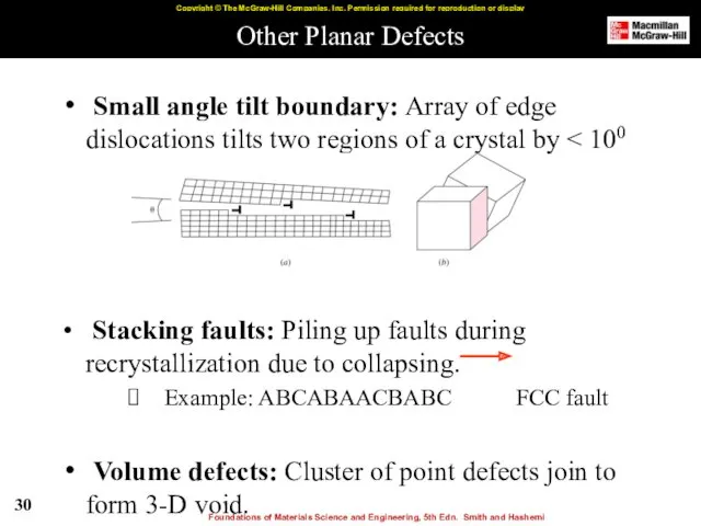
Other Planar Defects
Small angle tilt boundary: Array of edge dislocations
Other Planar Defects
Small angle tilt boundary: Array of edge dislocations
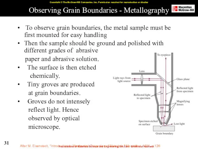
Observing Grain Boundaries - Metallography
To observe grain boundaries, the metal
Observing Grain Boundaries - Metallography
To observe grain boundaries, the metal
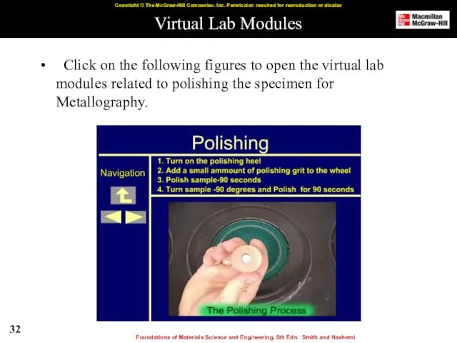
Virtual Lab Modules
Click on the following figures to open the
Virtual Lab Modules
Click on the following figures to open the
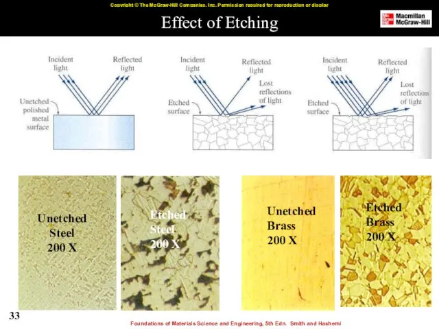
Effect of Etching
Unetched
Steel
200 X
Etched
Steel
200 X
Unetched
Brass
200 X
Etched
Brass
200 X
Effect of Etching
Unetched
Steel
200 X
Etched
Steel
200 X
Unetched
Brass
200 X
Etched
Brass
200 X
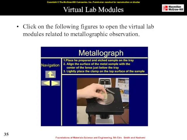
Virtual Lab Modules
Click on the following figures to open the virtual
Virtual Lab Modules
Click on the following figures to open the virtual
Virtual Lab Modules
Click on the following figures to open the virtual
Virtual Lab Modules
Click on the following figures to open the virtual
Grain Size
Affects the mechanical properties of the material
The smaller
Grain Size
Affects the mechanical properties of the material
The smaller
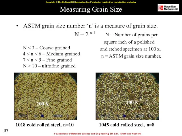
Measuring Grain Size
ASTM grain size number ‘n’ is a
Measuring Grain Size
ASTM grain size number ‘n’ is a
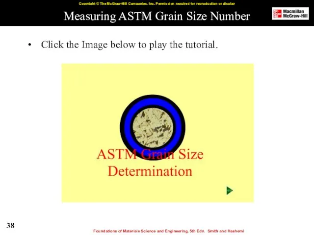
Measuring ASTM Grain Size Number
Click the Image below to play
Measuring ASTM Grain Size Number
Click the Image below to play
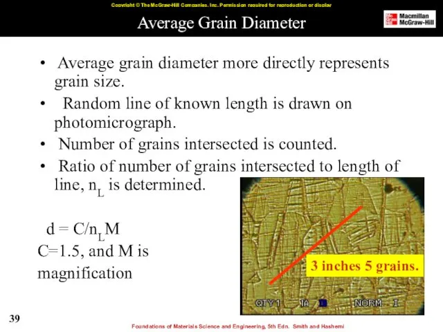
Average Grain Diameter
Average grain diameter more directly represents grain size.
Average Grain Diameter
Average grain diameter more directly represents grain size.
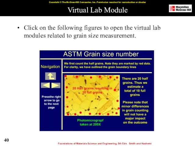
Virtual Lab Module
Click on the following figures to open the virtual
Virtual Lab Module
Click on the following figures to open the virtual
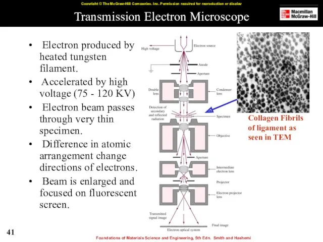
Transmission Electron Microscope
Electron produced by heated tungsten filament.
Accelerated by
Transmission Electron Microscope
Electron produced by heated tungsten filament.
Accelerated by
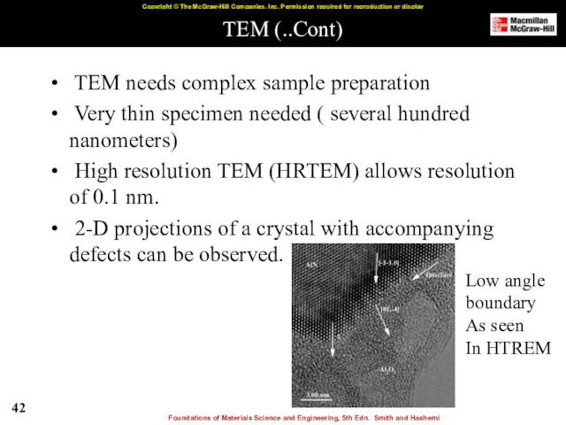
TEM (..Cont)
TEM needs complex sample preparation
Very thin specimen needed
TEM (..Cont)
TEM needs complex sample preparation
Very thin specimen needed
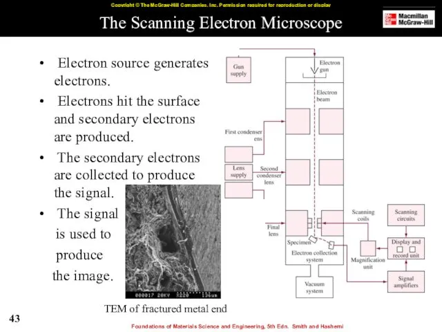
The Scanning Electron Microscope
Electron source generates electrons.
Electrons hit the
The Scanning Electron Microscope
Electron source generates electrons.
Electrons hit the
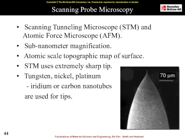
Scanning Probe Microscopy
Scanning Tunneling Microscope (STM) and Atomic Force Microscope
Scanning Probe Microscopy
Scanning Tunneling Microscope (STM) and Atomic Force Microscope
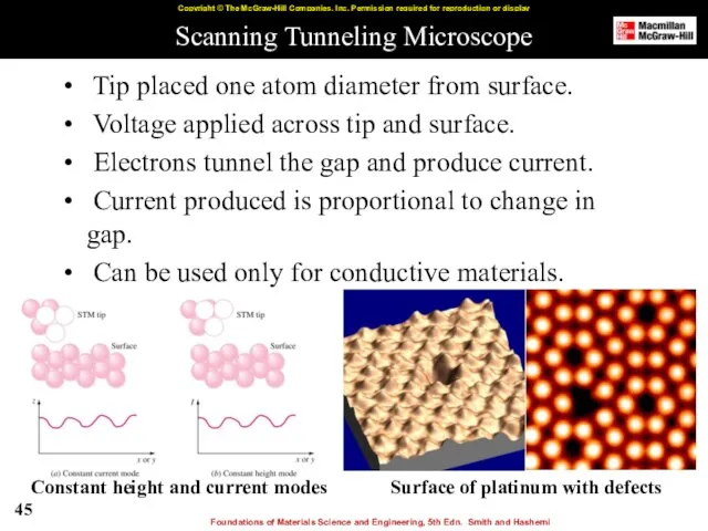
Scanning Tunneling Microscope
Tip placed one atom diameter from surface.
Voltage
Scanning Tunneling Microscope
Tip placed one atom diameter from surface.
Voltage
 презентация Введение в предмет
 Методы электрохимической поляризации
 Интеллектуальная игра по физике для 7 класса Умники и умницы
 Передача информации с помощью электромагнитных волн
 Геоэлектрика. (Лекция 7)
 Физический диктант по теме Электромагнитные колебания
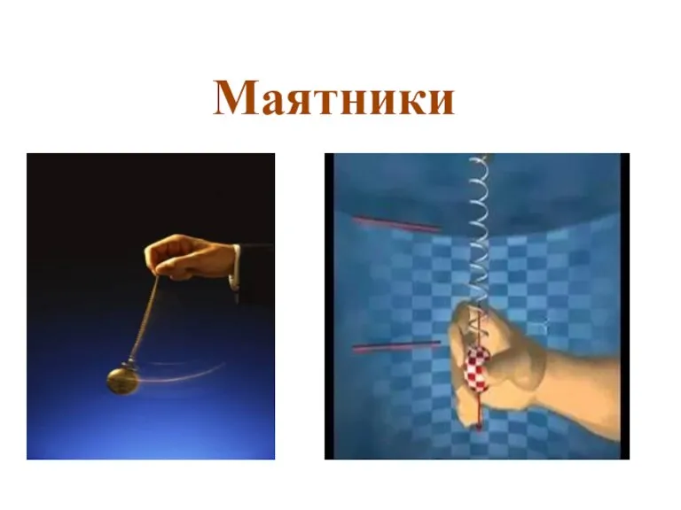 Маятники. Види маятників
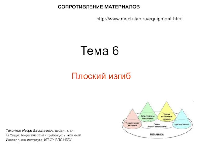 Плоский изгиб
 Сварные соединения
 Содержание курса физики основной школы наше время
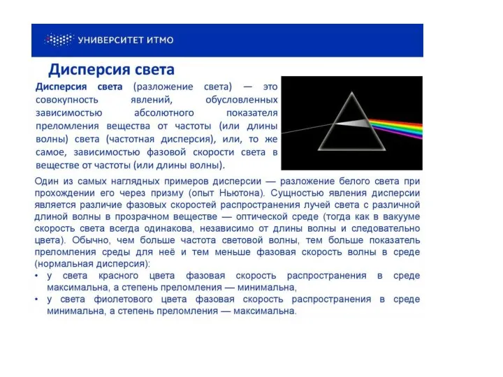 Дисперсия света
 презентация к уроку Волновая и корпускулярная теория света
 Көлікті пайдалану және жүк қозғалысы мен тасымалдауды ұйымдастыру
 Общие сведения и классификация трансформатора. (Тема 4)
 МКТ.Своя игра
 Гидравлические машины. 7 класс
 Электронные курсы. Материаловедение. Техническая механика
 Кинематика вращательного движения абсолютно твердого тела
 Строение атомов и молекул химического вещества с позиции квантовой теории
 Интегрированный урок физики и поэзии
 Физика – фундаментальная наука о природе
 Элементы игр на уроках физики
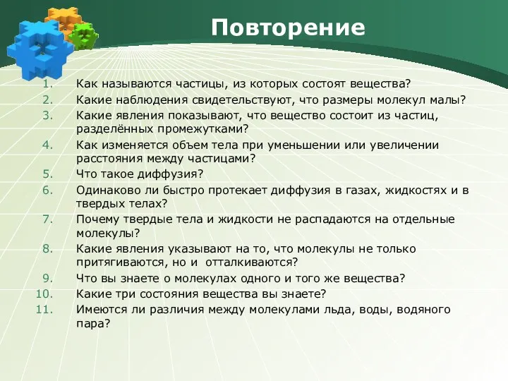 Как называются частицы, из которых состоят вещества?
 Спектральный анализ
 Замедление нейтронов. Уравнение переноса
 Потенциал электрического поля
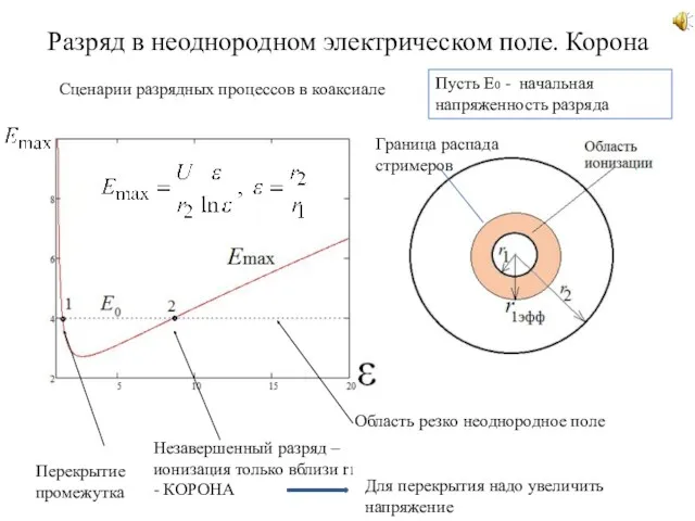 Разряд в неоднородном электрическом поле. Корона. Сценарии разрядных процессов в коаксиале. (Лекция 3)
 Механические волны