- Microcontrollers board misis board 877

Содержание
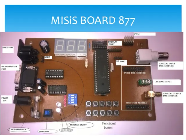
- 2. MISiS BOARD 877
- 3. PCB
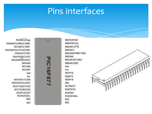
- 4. Pins interfaces
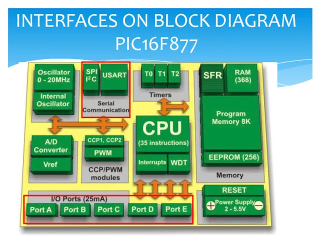
- 5. INTERFACES ON BLOCK DIAGRAM PIC16F877
- 6. Schematic diagram
- 7. 2 groups 5 channels Write «1» - active group Reed «1» - touch button Connections button
- 8. 2 groups 5 channels Write «1» - active group Reed «1» - touch button Connections LED
- 9. Connectors
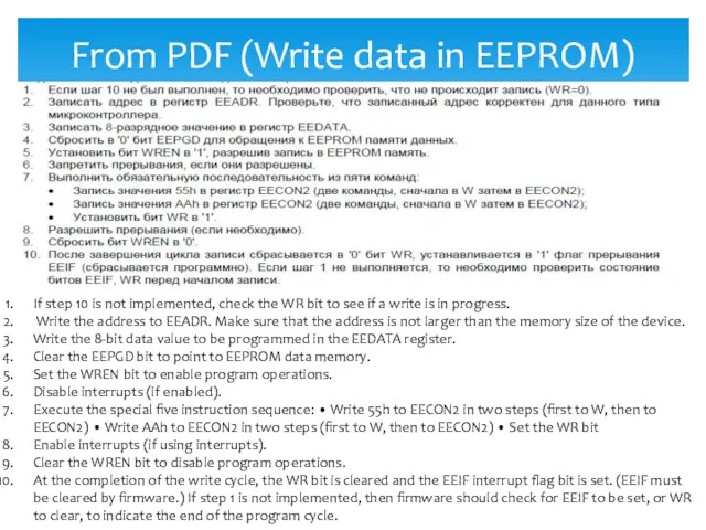
- 10. From PDF (Write data in EEPROM) If step 10 is not implemented, check the WR bit
- 11. void ZAP_N(void) { while(WR == 1) //wait, when ends past record ; //empty string, waiting until
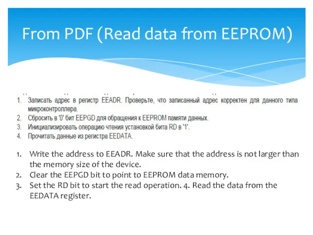
- 12. From PDF (Read data from EEPROM) Write the address to EEADR. Make sure that the address
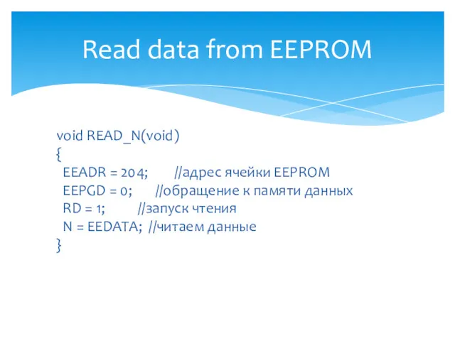
- 13. Read data from EEPROM void READ_N(void) { EEADR = 204; //адрес ячейки EEPROM EEPGD = 0;
- 14. personal task
- 15. Random digit 1-6 and send UART. 1 Button , UART. Touch button for count digits 1-6.
- 16. Block Diagram Start Initialisations Reed port currstat == 1 counter ++ prevstat == 1 currstat ==
- 17. CODE C #include __CONFIG(0x03F72); char curstat; //текущее состояние char oldstat; //старое состояние char counter=1; void Delay(int
- 19. Скачать презентацию
MISiS BOARD 877
MISiS BOARD 877
PCB
PCB
Pins interfaces
Pins interfaces
INTERFACES ON BLOCK DIAGRAM
PIC16F877
INTERFACES ON BLOCK DIAGRAM
PIC16F877
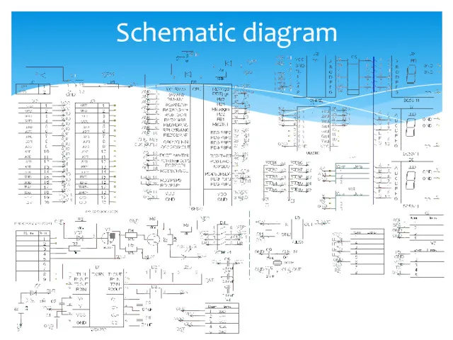
Schematic diagram
Schematic diagram
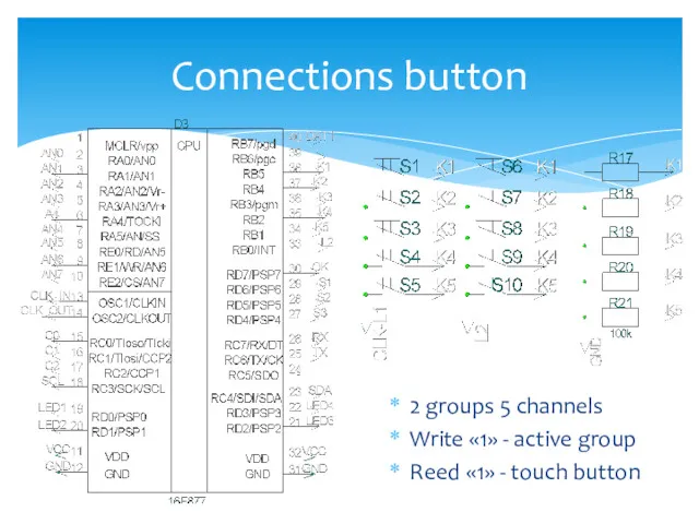
2 groups 5 channels
Write «1» - active group
Reed «1» - touch
2 groups 5 channels
Write «1» - active group
Reed «1» - touch
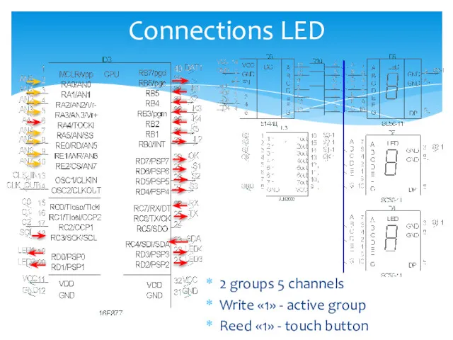
2 groups 5 channels
Write «1» - active group
Reed «1» - touch
2 groups 5 channels
Write «1» - active group
Reed «1» - touch
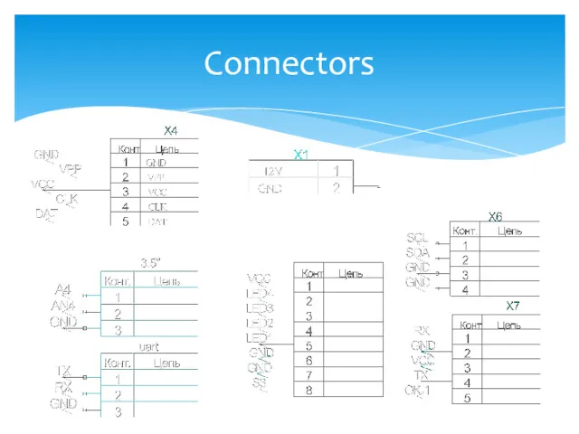
Connectors
Connectors
From PDF (Write data in EEPROM)
If step 10 is not implemented,
From PDF (Write data in EEPROM)
If step 10 is not implemented,
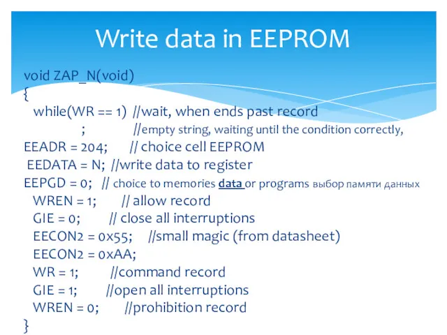
void ZAP_N(void)
{
while(WR == 1) //wait, when ends past record
;
void ZAP_N(void)
{
while(WR == 1) //wait, when ends past record
;
From PDF (Read data from EEPROM)
Write the address to EEADR. Make
From PDF (Read data from EEPROM)
Write the address to EEADR. Make
Read data from EEPROM
void READ_N(void)
{
EEADR = 204; //адрес ячейки EEPROM
Read data from EEPROM
void READ_N(void)
{
EEADR = 204; //адрес ячейки EEPROM
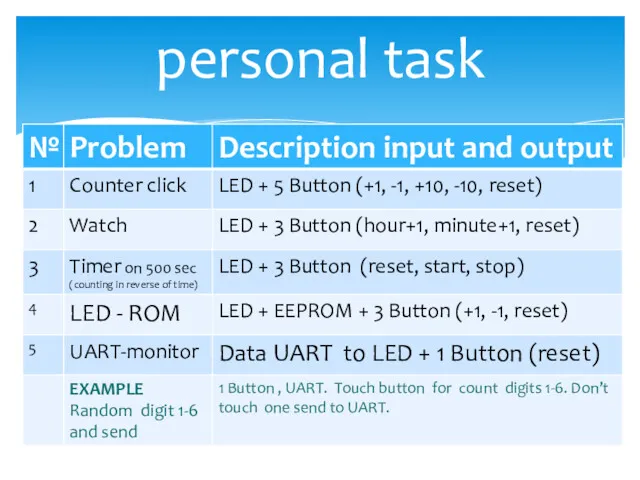
personal task
personal task
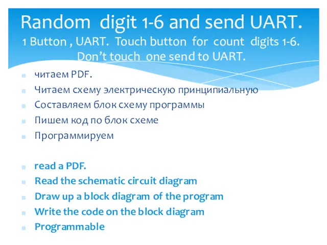
Random digit 1-6 and send UART.
1 Button , UART. Touch button
Random digit 1-6 and send UART. 1 Button , UART. Touch button
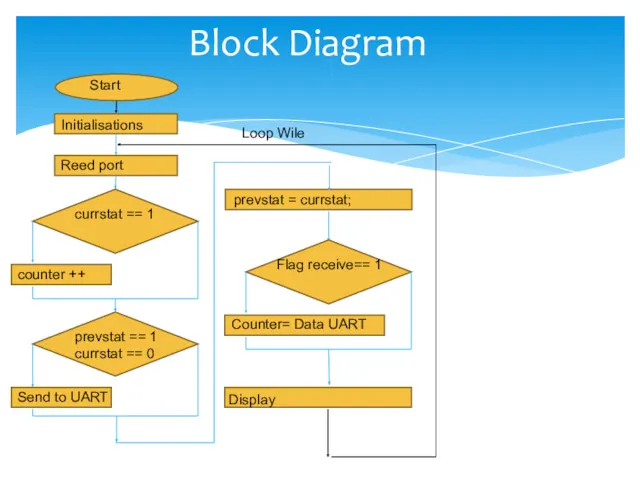
Block Diagram
Start
Initialisations
Reed port
currstat == 1
counter ++
prevstat == 1 currstat == 0
Send
Block Diagram
Start
Initialisations
Reed port
currstat == 1
counter ++
prevstat == 1 currstat == 0
Send
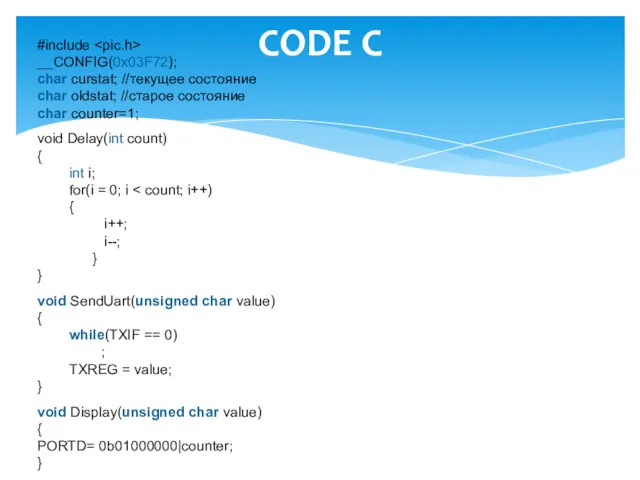
CODE C
#include
__CONFIG(0x03F72);
char curstat; //текущее состояние
char oldstat; //старое состояние
char counter=1;
void Delay(int
CODE C
#include
__CONFIG(0x03F72);
char curstat; //текущее состояние
char oldstat; //старое состояние
char counter=1;
void Delay(int
 Где искать научно-техническую информацию?
 Графический дизайн и мультимедиа. Динамическая графика
 Жизненный цикл программного обеспечения. Модели ЖЦ ПО
 Урок решения задач по теме Файл и файловая система
 Интенсив-курс по React JS. Занятие 1. Основы React
 Проектирование баз данных. Введение
 Методика и практика создания Интернет-магазинов в системе CMS 1С-Битрикс: Управление сайтом - Бизнес
 А что такое ОС?
 Устройства и способы потребления новостей
 Проектирование информационных систем
 Кодирование звуковой информации
 Основные понятия и определения. Основы программирования и баз данных www.specialist.ru
 Компьютерные технологии. Версия Matlab R2013b
 Создание презентаций в Microsoft Power Point
 Знакомство с OpenGL. Графические функции
 Помогаем экономить рабочее время при звонках
 Программирование на Python
 Python. Оператор присваивания
 Электронная почта. Сетевое коллективное взаимодействие и сетевой этикет
 Архиваторы
 Презантация по информатике Моделирование как метод познания
 Графические возможности Pascal
 Информация и энтропия
 Интернет-воздействие и проблемы трезвости современной молодежи
 მონაცემთა ბაზები
 Оператор варианта
 Настройка маршрутизаторов DIR-300 и DIR-400 для работы в сети провайдера SKYNET* при помощи авторизатора
 Introduction to the course. Managing the application life cycle