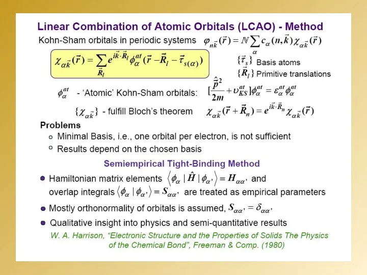
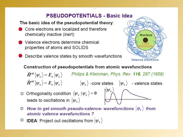
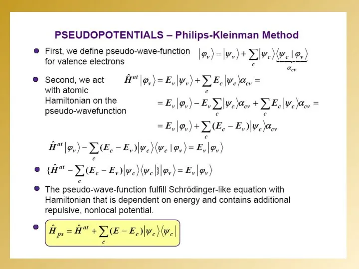
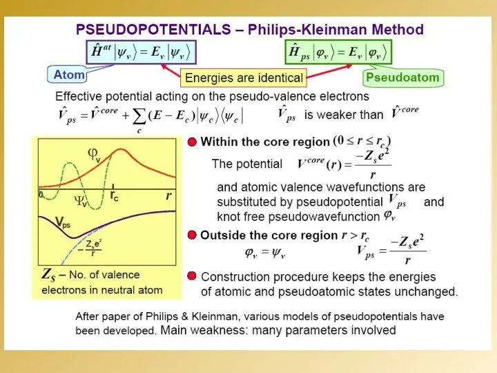
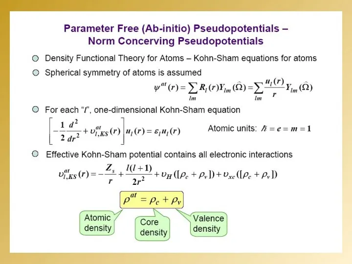
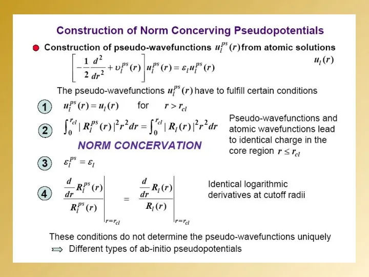
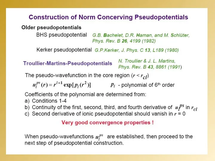
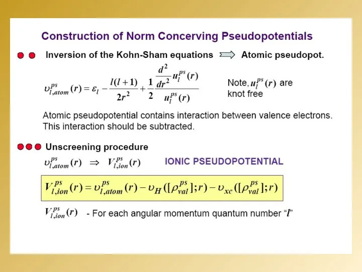
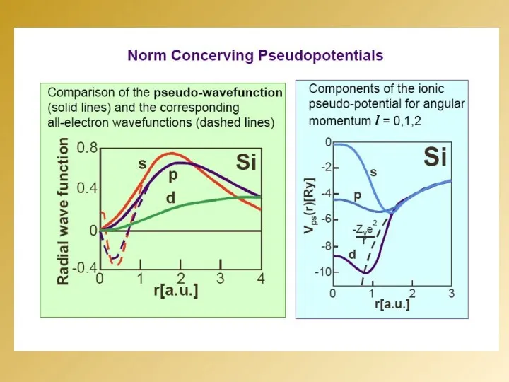
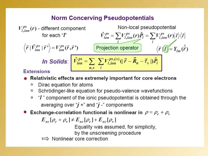
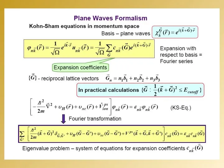
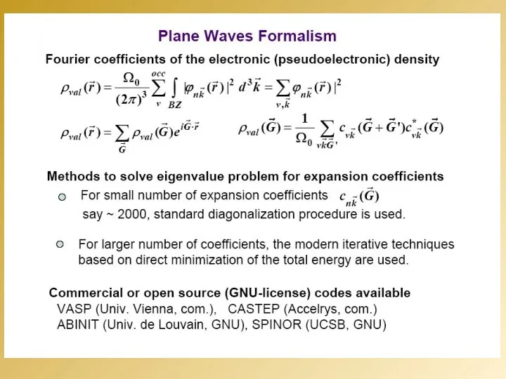
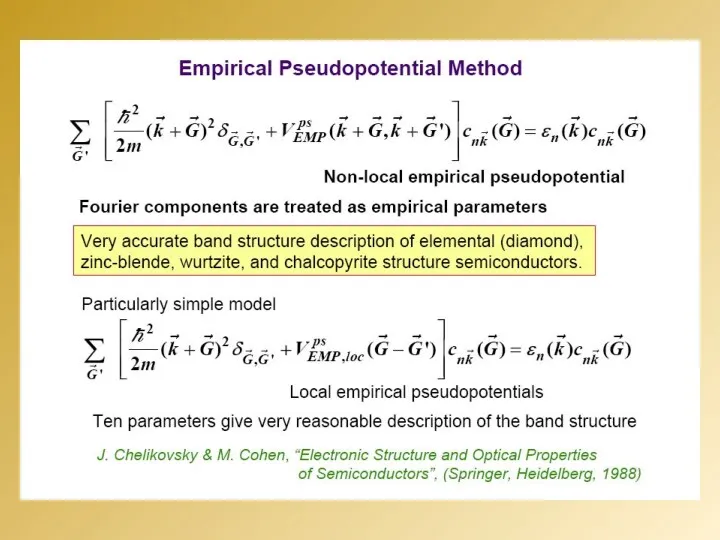
- Practical application of the method of Kona-Shema. Pseudopotentials method

Содержание
- 7. Выводы
- 24. The large number of surface structures observed on III-V (001) surfaces have early on prompted attempts
- 25. Computational details P. Blaha, K. Schwarz et al. An augmented Plane Wave + Local Orbitals Program
- 26. * - S.Lee, S. Lee, M. Scheffler. PRB 69, 125317 (2004) (FHI) ** - G. Qian,
- 27. Models of Ga-terminated GaAs(001)-(4х2) surface
- 28. ELECTRONIC STRUCTURE Two dimensional Brillouin zone (a) and E(k) for Ga-terminated β2- (b) and ζ-GaAs(001)-(4×2) (c),
- 29. ζ-GaAs(001)-(4×2) Adsorption on ζ-GaAs(001)-(4×2) The position of adsorbates (cesium and chlorine) on surface ζ-GaAs(001)-(4×2) after relaxation
- 30. Adsorption energies of Cs and Cl on Ga-terminated ζ-GaAs(001)-(4×2) surface * S.M. Lee, S.H. Lee, M.
- 31. Strong hybridization of As and Ga p-states with Cl p-orbitals together with weak s-s hybridization is
- 32. Cs on Ga-terminated ζ-GaAs(001)-(4×2) E(k) for clean surface and Cs in М1, S4, S5 sites and
- 33. М1,М2 S1, S2 S3, S4 M1 The orbital composition of wave function and their localization on
- 34. The charge difference for Cs in M1 –M3, S1, S5, S6 positions on Ga- terminated ζ-GaAs(001)-(4×2).
- 35. The charge difference for Cl in M1 –M3, S1, S5, S6 positions on Ga-terminated ζ-GaAs(001)-(4×2). X
- 36. Charge transfer Integrated Cs valence charge difference as function of integration radius for different adsorption sites
- 37. The adsorption energies of Cs for S1 and S2 sites on ζ-GaAs(001)-(4×2) with adsorbed Cs in
- 38. Charge transfer Integrated valence charge difference as a function of spheres radius for ζ-GaAs(001)-(4×2) with two
- 39. Cs on ζ-GaAs(001)-(4×2) E(k) for ζ–GaAs(001)–(4×2) with Cs adsorbed in S5 site (a), with two Cs
- 40. Electronic structure of (Cs-O)/GaAs(001) interface Models of (Cs-O)/GaAs(001) interface Total, local surface DOS of ζ-GaAs(001)-(4×2) with
- 41. Calculated STM images of filled and empty states: I adsorbed in the M1 position on ζ-GaAs(001)-(4×2)
- 42. Calculated STM images: clean ζ-GaAs(001)-(4×2) U =-1.5 V (filled) U =1.8 V (empty) S.H. Lee et
- 44. Скачать презентацию

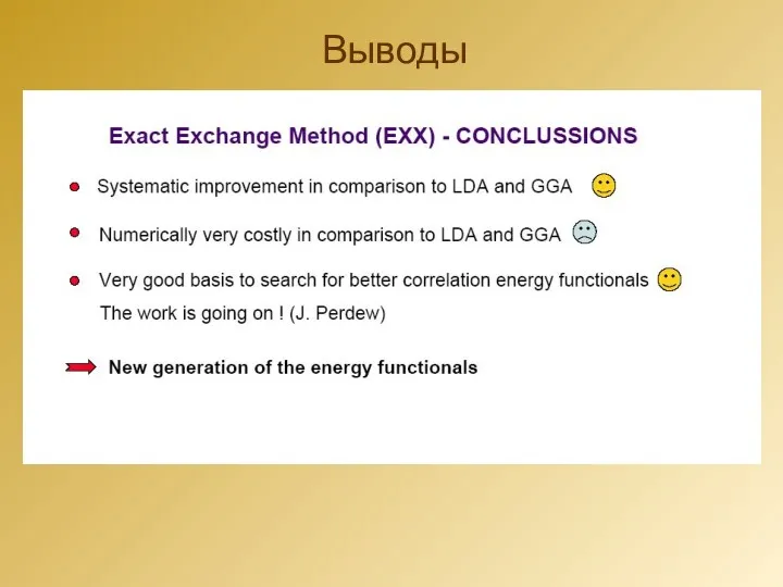
Выводы
Выводы
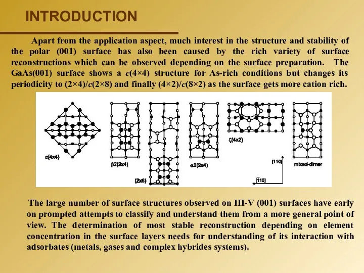
The large number of surface structures observed on III-V (001) surfaces
The large number of surface structures observed on III-V (001) surfaces
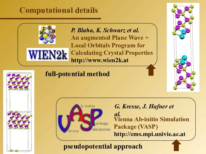
Computational details
P. Blaha, K. Schwarz et al.
An augmented Plane Wave
Computational details
P. Blaha, K. Schwarz et al.
An augmented Plane Wave
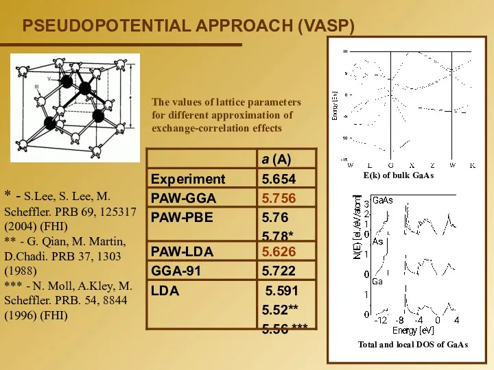
* - S.Lee, S. Lee, M. Scheffler. PRB 69, 125317 (2004)
* - S.Lee, S. Lee, M. Scheffler. PRB 69, 125317 (2004)
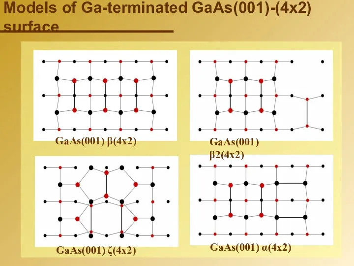
Models of Ga-terminated GaAs(001)-(4х2) surface
Models of Ga-terminated GaAs(001)-(4х2) surface
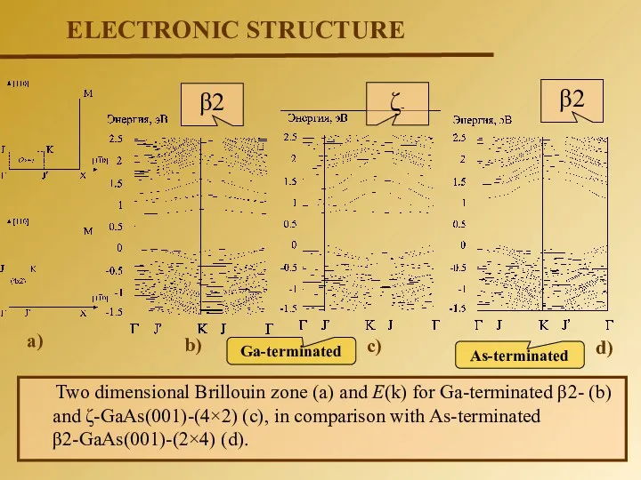
ELECTRONIC STRUCTURE
Two dimensional Brillouin zone (a) and E(k) for
ELECTRONIC STRUCTURE
Two dimensional Brillouin zone (a) and E(k) for
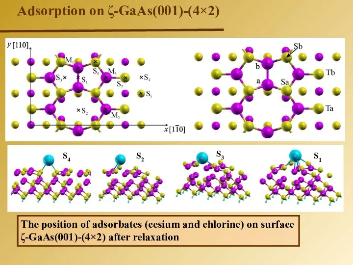
ζ-GaAs(001)-(4×2)
Adsorption on ζ-GaAs(001)-(4×2)
The position of adsorbates (cesium
ζ-GaAs(001)-(4×2)
Adsorption on ζ-GaAs(001)-(4×2)
The position of adsorbates (cesium
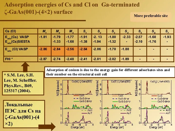
Adsorption energies
Adsorption energies
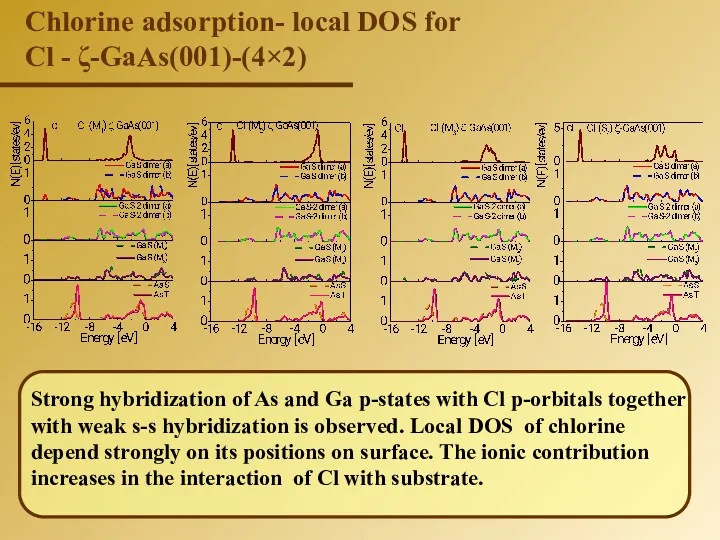
Strong hybridization of As and Ga p-states with Cl
Strong hybridization of As and Ga p-states with Cl
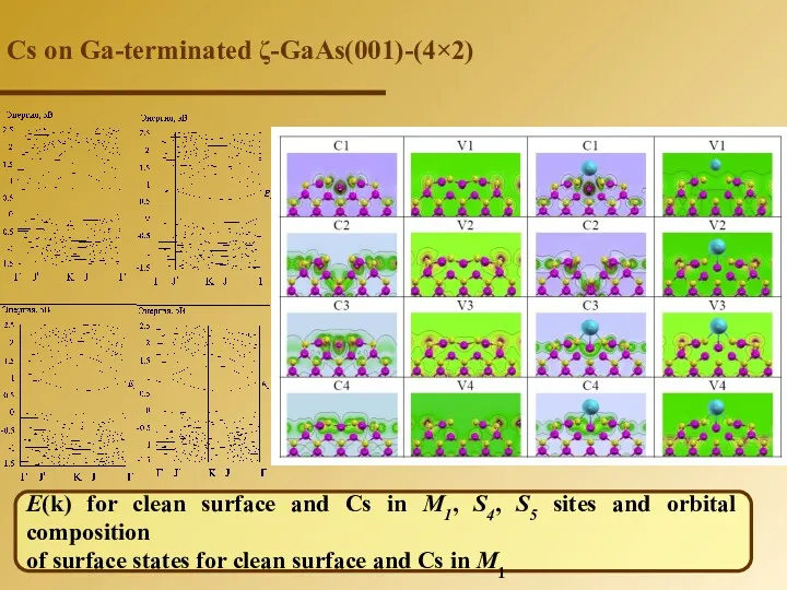
Cs on Ga-terminated ζ-GaAs(001)-(4×2)
E(k) for clean surface
Cs on Ga-terminated ζ-GaAs(001)-(4×2)
E(k) for clean surface
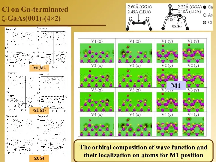
М1,М2
S1, S2
S3, S4
M1
The orbital composition of wave
М1,М2
S1, S2
S3, S4
M1
The orbital composition of wave
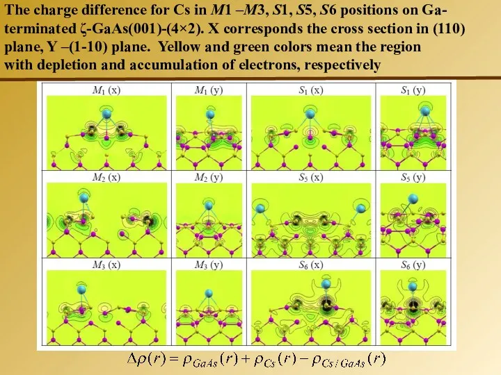
The charge difference for Cs in M1 –M3, S1, S5, S6
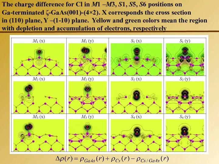
The charge difference for Cl in M1 –M3, S1, S5, S6
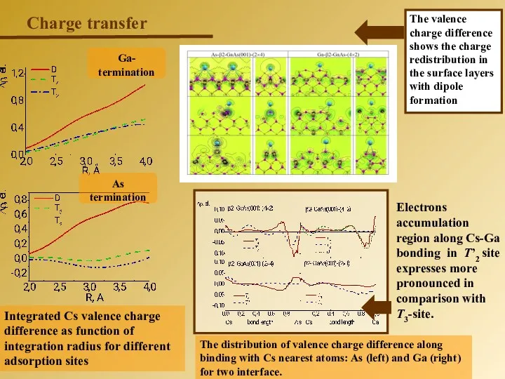
Charge transfer
Integrated Cs valence charge difference as function of integration radius
Charge transfer
Integrated Cs valence charge difference as function of integration radius
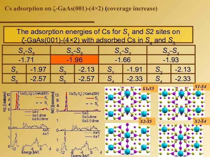
The adsorption energies of Cs for S1 and S2 sites on
The adsorption energies of Cs for S1 and S2 sites on
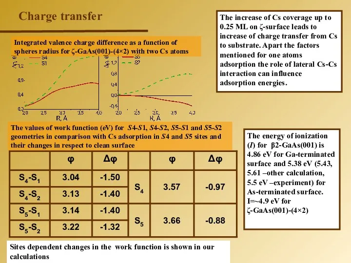
Charge transfer
Integrated valence charge difference as a function of spheres radius
Charge transfer
Integrated valence charge difference as a function of spheres radius
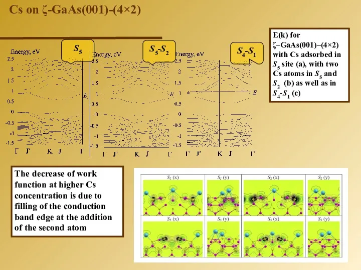
Cs on ζ-GaAs(001)-(4×2)
E(k) for ζ–GaAs(001)–(4×2) with Cs adsorbed in
Cs on ζ-GaAs(001)-(4×2)
E(k) for ζ–GaAs(001)–(4×2) with Cs adsorbed in
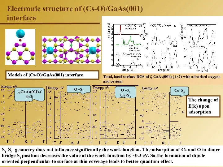
Electronic structure of (Cs-O)/GaAs(001) interface
Models of (Cs-O)/GaAs(001) interface
Electronic structure of (Cs-O)/GaAs(001) interface
Models of (Cs-O)/GaAs(001) interface
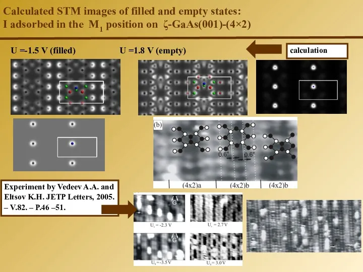
Calculated STM images of filled and empty states:
I adsorbed in the
Calculated STM images of filled and empty states:
I adsorbed in the
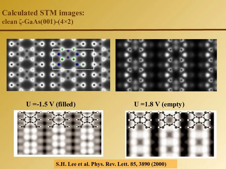
Calculated STM images:
clean ζ-GaAs(001)-(4×2)
U =-1.5 V (filled) U =1.8
Calculated STM images:
clean ζ-GaAs(001)-(4×2)
U =-1.5 V (filled) U =1.8
 Випадковий вектор. Граничні теореми теорії ймовірності
 Математика. Дополни примеры цифрами Устный счет.
 Старинные меры измерения длины
 Осевая и центральная симметрия. Урок геометрии в 8 классе
 Урок математики 4 класс. Урок-расследование Дело о пропавшем торте
 Деление с остатком. 5 класс
 Векторы в пространстве и действия над ними. Компланарные векторы. Тема 12
 Линейная функция и её график. Алгебра, урок № 24
 Теория кривых. Плоские кривые
 Презентация по внеурочной деятельности Математика и конструирование
 Занимательная математика
 Сложение и вычитание обыкновенных дробей с разными знаменателями
 Использование современных технологий для повышения качества математического образования
 Алгоритм решения задач на пропорции
 Коэффициент корреляции рангов Спирмена. Случай одинаковых рангов
 Составление числовых выражений с презентацией. УМК Начальная школа 21 века.
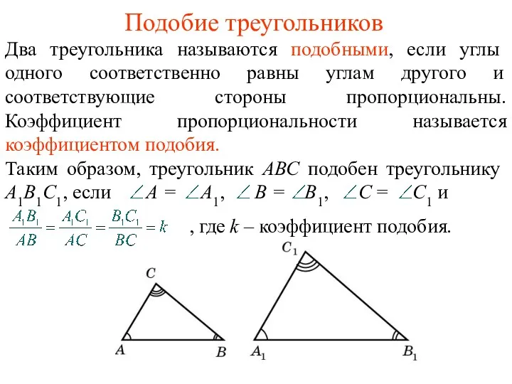 Первый признак подобия треугольников
 Сложение и вычитание десятичных дробей
 Ситуационная задача Устный счет – гимнастика ума
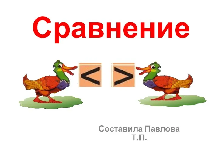 математика 1 класс Сравнение
 Расчет относительного риска (ОР) с использованием таблицы 2х2
 Множители, произведение.
 Многогранники. Урок 1. Определение и виды многогранников. Геометрия. 10 класс
 Решение уравнений с помощью разложения на множители. 7 класс
 Урок математики
 Обратная задача теории аппроксимации
 Смешанные числа. 5 класс
 Определённый интеграл. Приложения определенного интеграла