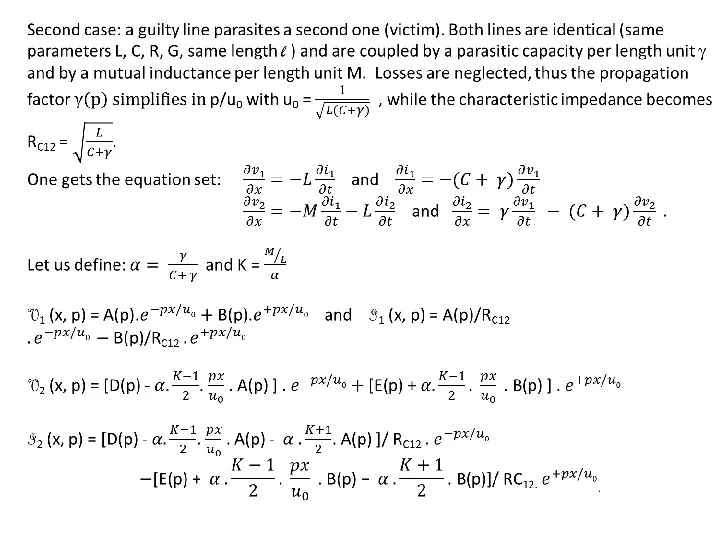
- EMI introduction & Coupling modes in EMI 2018-V1

Содержание
- 2. Schedule _ Introduction _ Electromagnetic environment _ How to take EMI into account _ How to
- 3. EMI : Context & stakes Context : Noisy environment owing to : More devices in an
- 5. Example: 1967: VIETNAM USS Forestal disaster A missile had been launched and directed towards aircraft carrier
- 6. Falkland’s War (1982): H.M.S. Sheffield aircraft carrier destroyed. Destruction by an enemy missile, as the missile
- 7. Destruction of F15 US Army plane due to a simple electrostatic discharge (ESD) 2 deads, one
- 8. In late 80’s, CB (Citizen Band) transmitters of trucks, very powerful, re-set to zero benzin pump
- 9. Motorized wheelchairs presented random movements and started untimely when firemen or policemen passed closely… Because :
- 10. Since 1905: first observations: perturbations from electronic devices can affect radio communications -> notions of parasite
- 11. 1934 : Creation of ISCRI (International Special Committee on Radio Interference) to establish limits, attempts proccesses
- 12. ELECTROMAGNETIC INTERFERENCES (EMI) : It is the aptitude of an equipment (or a system) to behave
- 13. Note that, in French, it is called Compatibilité électromagnétique which includes all points of view. In
- 14. Also, between victims and guilty devices, there exist 6 different modes of coupling, unfortunately acting often
- 15. External perturbations 1. Coupling by common impedance It is the only one coupling existing even in
- 16. In a general rule, the good mode to transmit informations is the differential mode, the one
- 17. Use ground plans, but be aware with skin effect and slits Impedance of a cupper plane
- 18. Cupper conductors L = 1 m With L length in m S section in mm2 Correctly
- 19. Parasitic voltage appearing are created in common mode To enhance EMI protection, one has to decrease
- 20. Currents flowing in the grounds of printed circuits can be reduced by a good decoupling of
- 21. Exercises: 1) For vehicles, sensors, systems, … are often supplied with 12 V DC, through a
- 22. 3) Explain on a sketch, presenting for example 2 devices (2 amplifiers), what is the coupling
- 23. 5) Why is it necessary to mesh as much as possible the ground connections of the
- 24. 6) In an office building, a small computer and its printer are in the same room,
- 25. 2 - Coupling conductor – ground plan Electronic Circuit Ground plan Voltage source creating parasites Parasitic
- 26. 3 – Coupling field to wire Field E perturbating Parasitic currents One has to reduce the
- 27. 4 – Coupling field to loop It is still a radiated coupling only present in AC,
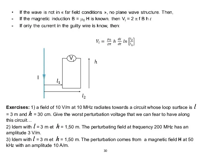
- 28. The field E is parallel to the loop, R too, then H and B are perpendicular
- 29. Then, the perturbation voltage amplitude is : Vi = 2 E0 h sin (k l /2).
- 30. Exercises: 1) a field of 10 V/m at 10 MHz radiates towards a circuit whose loop
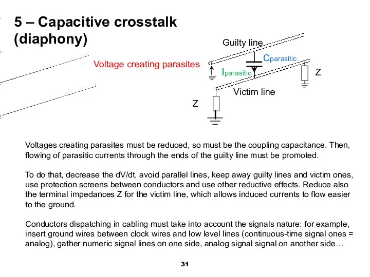
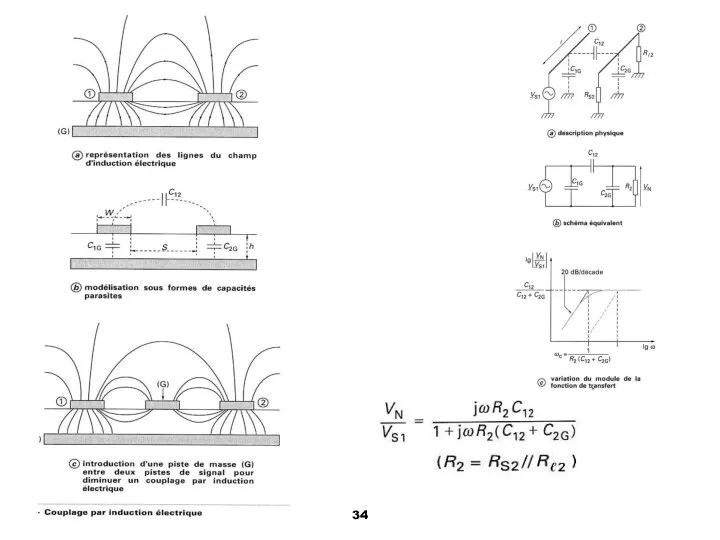
- 31. 5 – Capacitive crosstalk (diaphony) Cparasitic Guilty line Victim line Iparasitic Voltage creating parasites Z Voltages
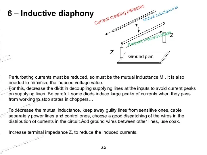
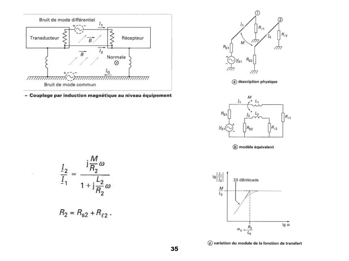
- 32. 6 – Inductive diaphony Perturbating currents must be reduced, so must be the mutual inductance M
- 33. Exercise: in comparing the coupling modes: diaphony by capacitive effects and diaphony by inductive effects, the
- 36. Differential mode (DM) and Common Mode (CM) : DM The differential mode: is the normal one
- 37. Differential mode (DM) and Common Mode (CM) :: The Common mode: the current flows with the
- 38. Measures in differential mode and in common mode : Differential mode voltage is measured between the
- 39. Some solutions to prevent common mode propagation Protection by ferrites Solutions allow to avoid any mode
- 40. Insulation of the common mode by optocouplers, optic linkages, special cables (with a conductor polymer sheath),
- 41. Here are 2 coils said as « common mode coils » : their inductances are much
- 42. Filters on supplying devices: Placed on insulator. Pig tail. Inputs and outputs too close Placed on
- 45. Скачать презентацию
Schedule
_ Introduction
_ Electromagnetic environment
_ How to take EMI into account
_ How
Schedule
_ Introduction
_ Electromagnetic environment
_ How to take EMI into account
_ How
EMI : Context & stakes
Context :
Noisy environment owing to :
More devices
EMI : Context & stakes
Context :
Noisy environment owing to :
More devices
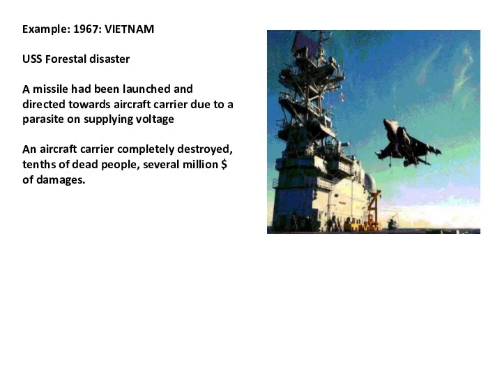
Example: 1967: VIETNAM
USS Forestal disaster
A missile had been launched and directed
Example: 1967: VIETNAM
USS Forestal disaster
A missile had been launched and directed
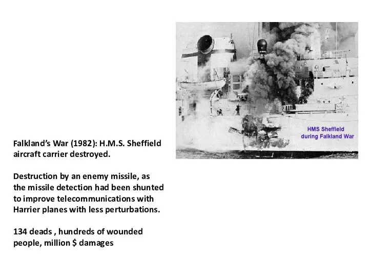
Falkland’s War (1982): H.M.S. Sheffield aircraft carrier destroyed.
Destruction by an enemy
Falkland’s War (1982): H.M.S. Sheffield aircraft carrier destroyed.
Destruction by an enemy
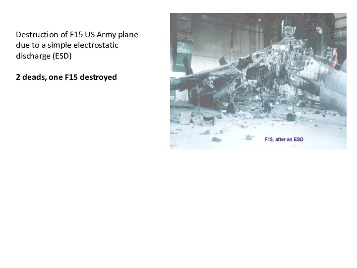
Destruction of F15 US Army plane due to a simple electrostatic
Destruction of F15 US Army plane due to a simple electrostatic
In late 80’s, CB (Citizen Band) transmitters of trucks, very powerful,
re-set
In late 80’s, CB (Citizen Band) transmitters of trucks, very powerful,
re-set
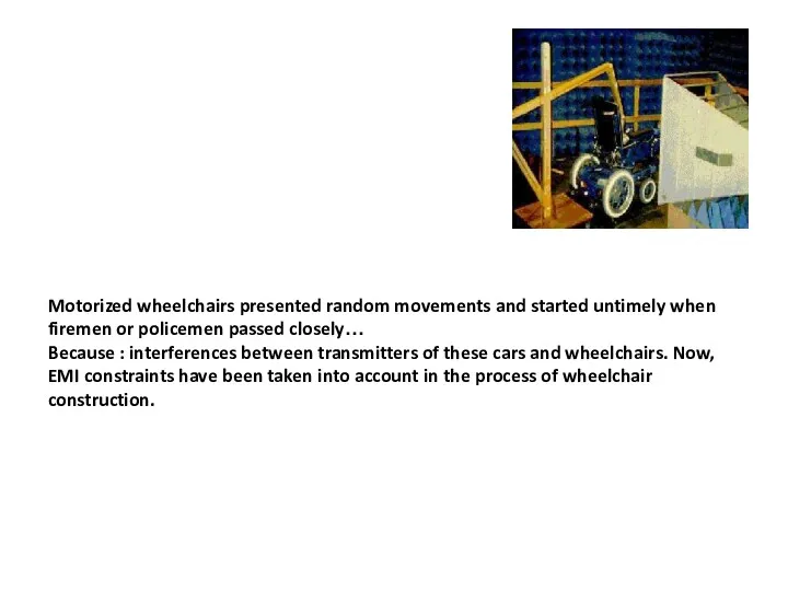
Motorized wheelchairs presented random movements and started untimely when firemen or
Motorized wheelchairs presented random movements and started untimely when firemen or
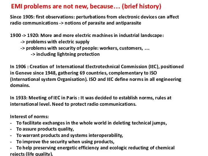
Since 1905: first observations: perturbations from electronic devices can affect
Since 1905: first observations: perturbations from electronic devices can affect
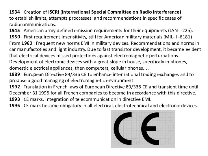
1934 : Creation of ISCRI (International Special Committee on Radio Interference)
to
1934 : Creation of ISCRI (International Special Committee on Radio Interference)
to
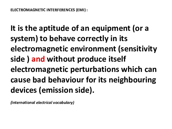
ELECTROMAGNETIC INTERFERENCES (EMI) :
It is the aptitude of an equipment (or
ELECTROMAGNETIC INTERFERENCES (EMI) :
It is the aptitude of an equipment (or
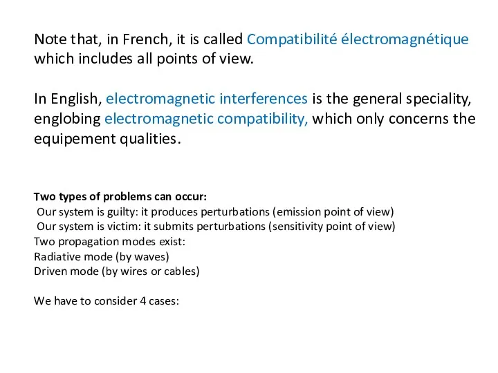
Note that, in French, it is called Compatibilité électromagnétique which includes
Note that, in French, it is called Compatibilité électromagnétique which includes
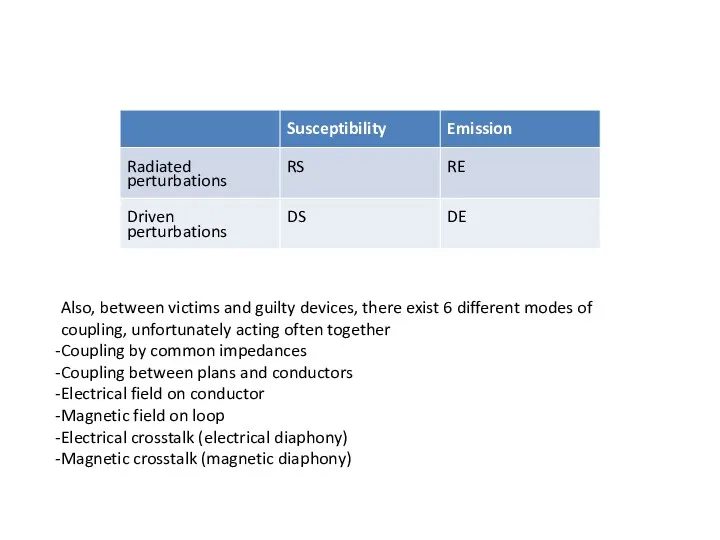
Also, between victims and guilty devices, there exist 6 different modes
Also, between victims and guilty devices, there exist 6 different modes
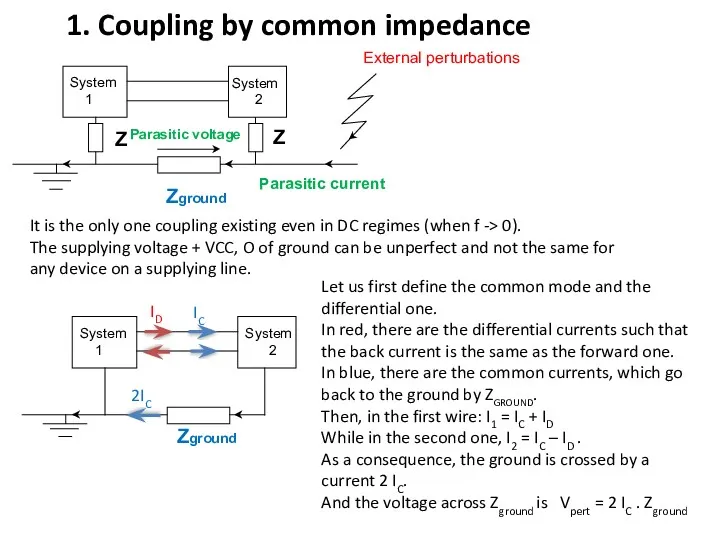
External perturbations
1. Coupling by common impedance
It is the only one
External perturbations
1. Coupling by common impedance
It is the only one
In a general rule, the good mode to transmit informations is
In a general rule, the good mode to transmit informations is
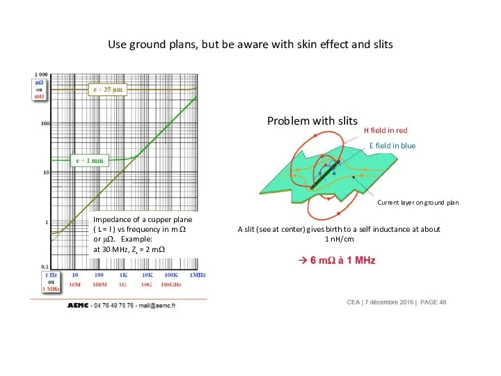
Use ground plans, but be aware with skin effect and slits
Impedance
Use ground plans, but be aware with skin effect and slits
Impedance
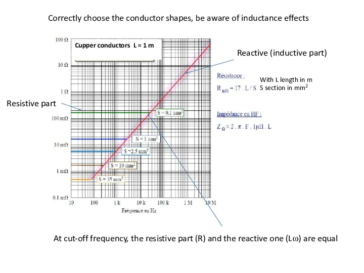
Cupper conductors L = 1 m
With L length in m
S section
Cupper conductors L = 1 m
With L length in m
S section
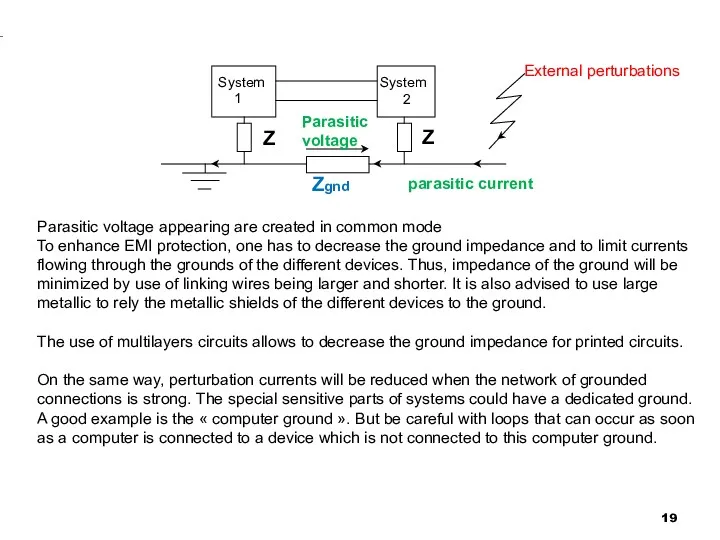
Parasitic voltage appearing are created in common mode
To enhance EMI protection,
Parasitic voltage appearing are created in common mode
To enhance EMI protection,
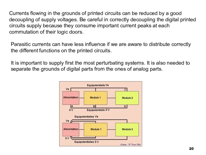
Currents flowing in the grounds of printed circuits can be reduced
Currents flowing in the grounds of printed circuits can be reduced
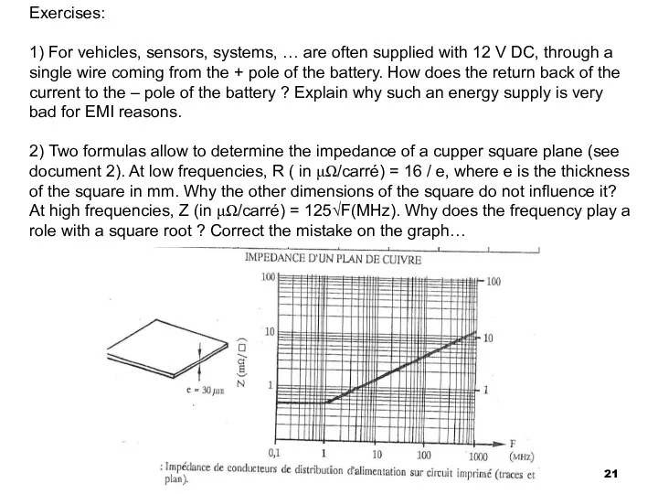
Exercises:
1) For vehicles, sensors, systems, … are often supplied with
Exercises:
1) For vehicles, sensors, systems, … are often supplied with
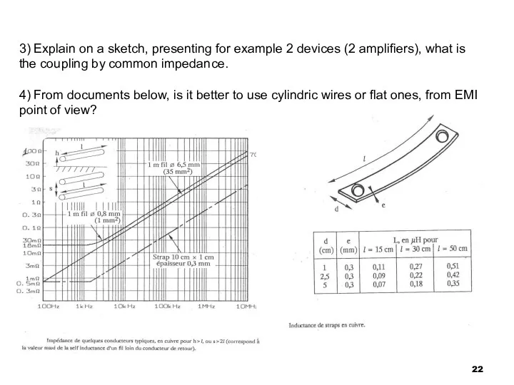
3) Explain on a sketch, presenting for example 2 devices (2
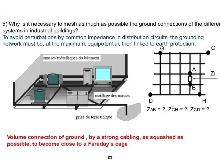
5) Why is it necessary to mesh as much as possible
5) Why is it necessary to mesh as much as possible
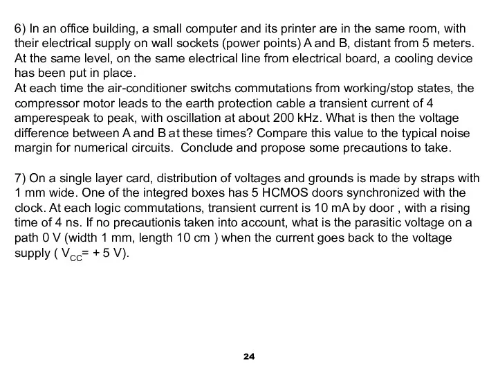
6) In an office building, a small computer and its printer
6) In an office building, a small computer and its printer
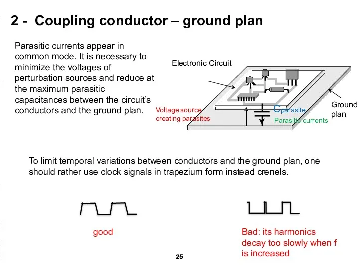
2 - Coupling conductor – ground plan
Electronic Circuit
Ground plan
Voltage source
2 - Coupling conductor – ground plan
Electronic Circuit
Ground plan
Voltage source
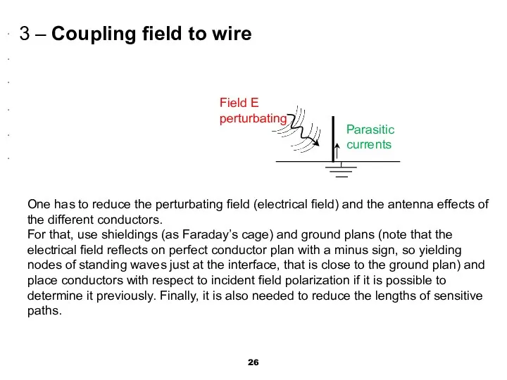
3 – Coupling field to wire
Field E perturbating
Parasitic currents
One
3 – Coupling field to wire
Field E perturbating
Parasitic currents
One
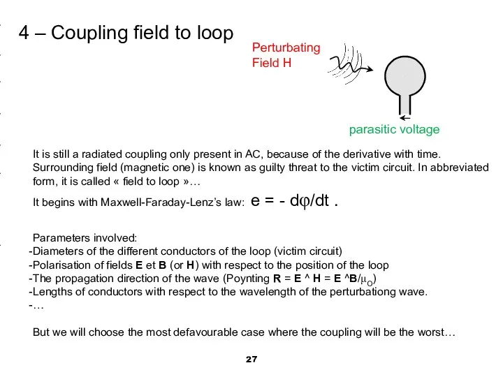
4 – Coupling field to loop
It is still a radiated coupling
4 – Coupling field to loop
It is still a radiated coupling
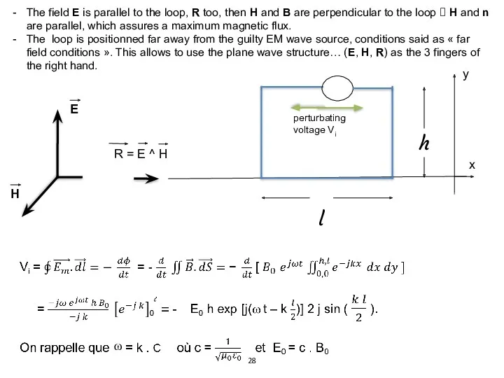
The field E is parallel to the loop, R too, then
The field E is parallel to the loop, R too, then
Then, the perturbation voltage amplitude is : Vi = 2 E0
Then, the perturbation voltage amplitude is : Vi = 2 E0
Exercises: 1) a field of 10 V/m at 10 MHz radiates
Exercises: 1) a field of 10 V/m at 10 MHz radiates
5 – Capacitive crosstalk (diaphony)
Cparasitic
Guilty line
Victim line
Iparasitic
Voltage creating parasites
Z
Voltages creating parasites
5 – Capacitive crosstalk (diaphony)
Cparasitic
Guilty line
Victim line
Iparasitic
Voltage creating parasites
Z
Voltages creating parasites
6 – Inductive diaphony
Perturbating currents must be reduced, so must be
6 – Inductive diaphony
Perturbating currents must be reduced, so must be
Exercise: in comparing the coupling modes: diaphony by capacitive effects and
Exercise: in comparing the coupling modes: diaphony by capacitive effects and
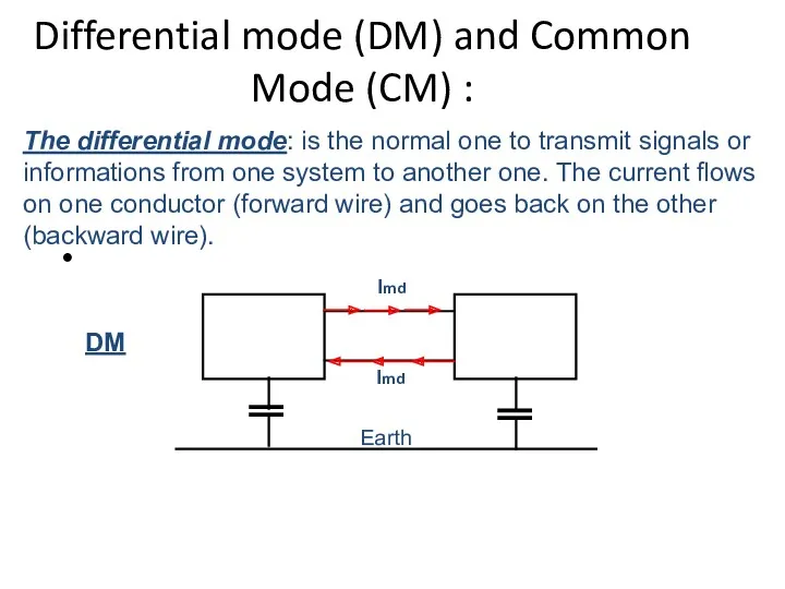
Differential mode (DM) and Common Mode (CM) :
DM
The differential mode: is
Differential mode (DM) and Common Mode (CM) :
DM
The differential mode: is
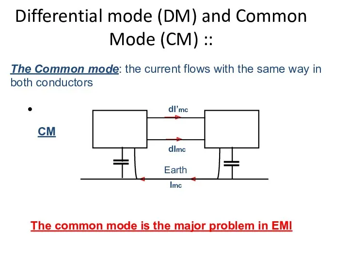
Differential mode (DM) and Common Mode (CM) ::
The Common mode: the
Differential mode (DM) and Common Mode (CM) ::
The Common mode: the
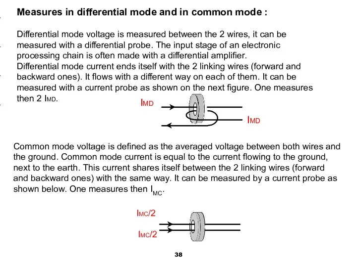
Measures in differential mode and in common mode :
Differential mode voltage is
Measures in differential mode and in common mode :
Differential mode voltage is
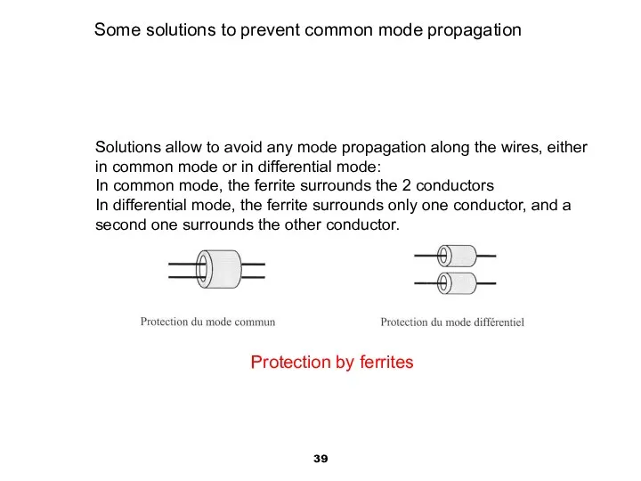
Some solutions to prevent common mode propagation
Protection by ferrites
Solutions
Some solutions to prevent common mode propagation
Protection by ferrites
Solutions
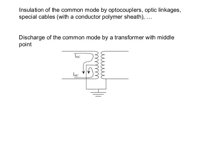
Insulation of the common mode by optocouplers, optic linkages, special cables
Insulation of the common mode by optocouplers, optic linkages, special cables
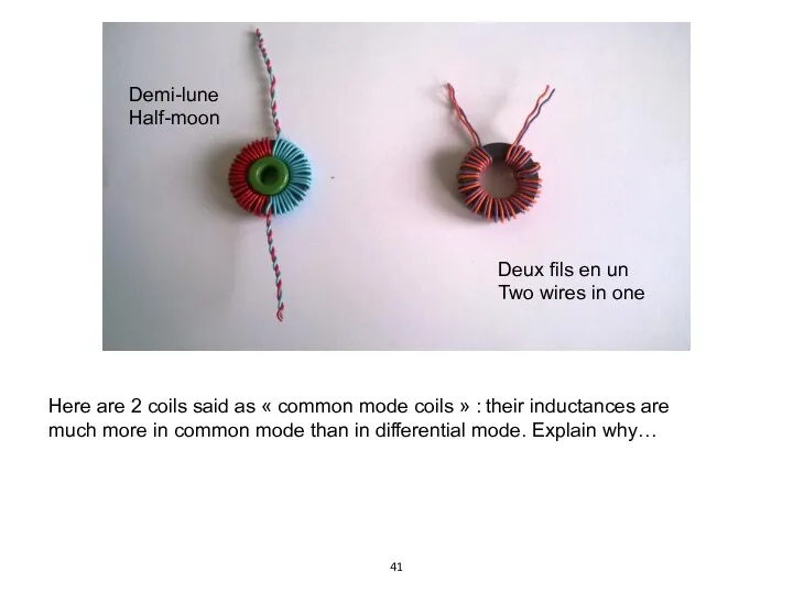
Here are 2 coils said as « common mode coils » : their
Here are 2 coils said as « common mode coils » : their
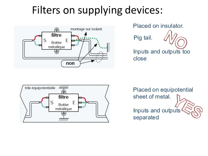
Filters on supplying devices:
Placed on insulator.
Pig tail.
Inputs and outputs
Filters on supplying devices:
Placed on insulator.
Pig tail.
Inputs and outputs
 Момент силы относительно центра
 Условия плавания тел. 7 класс
 Количество выпускников сдававших ЕГЭ по физике в 2011 г
 Динамика материальной точки
 Система P-Motronic
 Паровая машина
 Подсистемы системы Корабль. Подсистема Движение
 Научные открытия Ньютона в астрономии
 Авиационный механик (авиационный техник-механик, авиамеханик)
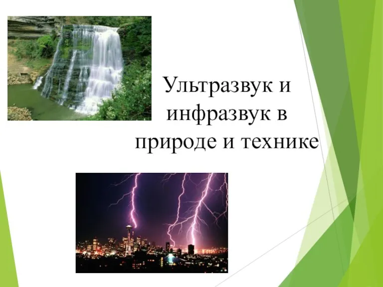 Ультразвук и инфразвук в природе и технике
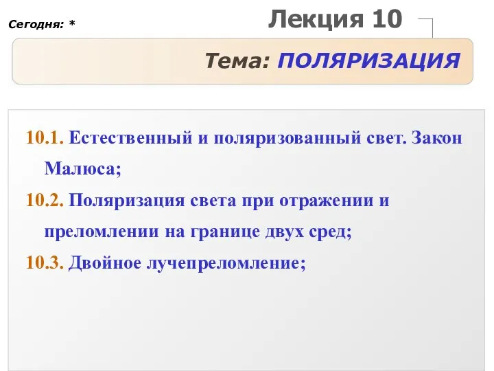 Лекция 10. Тема: поляризация
 Монтаж заземляющих устройств
 Динамика. Основные понятия
 Інерція та інертність. Маса та імпульс тіла. Другий закон Ньютона
 От энергии до...
 Решение задач. Закон сохранения заряда . Закон Кулона. Напряженность поля точечного заряда
 Электрическое поле в вакууме
 Тепломассообмен
 Линзы. Оптическая сила линзы
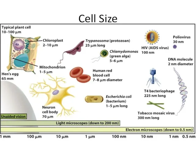 Microscope Measurement
 Введение в специальность
 Элементы машиноведения
 Публичная презентация.
 Магнитное поле
 Небольшое небесное тело комета
 Молекулярная физика и основы термодинамики
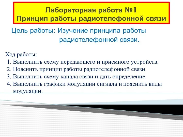 Принцип работы радиотелефонной связи
 Атомная физика