- Приборы полупроводниковой микро- и наноэлектроники

Содержание
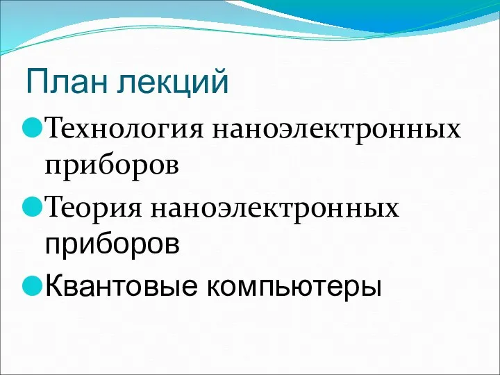
- 2. План лекций Технология наноэлектронных приборов Теория наноэлектронных приборов Квантовые компьютеры
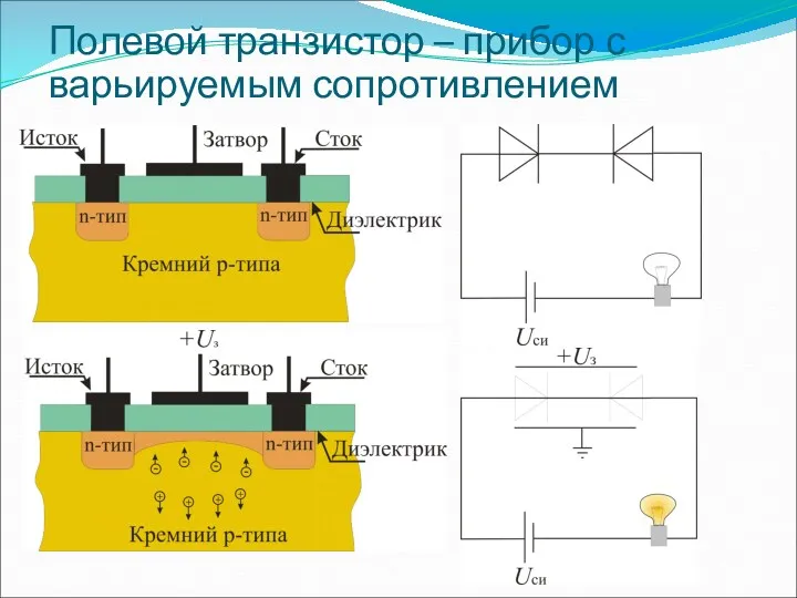
- 3. Полевой транзистор – прибор с варьируемым сопротивлением
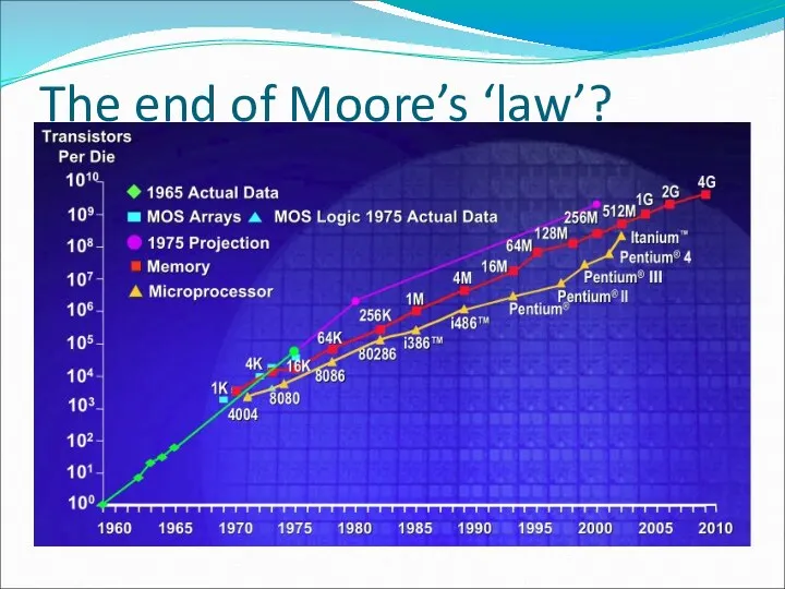
- 4. The end of Moore’s ‘law’?
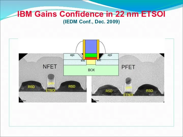
- 5. IBM Gains Confidence in 22 nm ETSOI (IEDM Conf., Dec. 2009)
- 6. Intel Going Vertical for 22nm Transistors in 2011
- 7. Multi-gate FETs N = 2 N = 3 N = 3,14 N = 3,4 N =
- 8. Экспериментальный технологический маршрут изготовления МДП КНИ - нанотранзистора Основные этапы изготовления : 1. Формирование STI изоляции;
- 9. Изготовление полевого транзистора
- 10. Изготовление полевого транзистора
- 11. Электронный литограф Raith-150 150x150mm stage for direct writing over 6” wafers Automatic airlock for sample loading
- 12. Аналитический автоэмиссионный растровый электронный микроскоп для исследования наноструктур ULTRA ZEISS
- 13. Установка атомно-слоевого осаждения FlexAl (Oxford Instruments Plasma Technology)
- 14. Установки фотолитографии (Zuss) и нанесения резиста (Sawatec)
- 15. Установка плазмохимического травления Plasma Lab 100 Dual (Oxford Instruments Plasma Technology)
- 16. Установка быстрого фотонного отжига Annealsys AS-100 Pyrometer and thermocouple control Fast digital PID temperature controller Temperature
- 17. Теория наноэлектронных приборов Требования современной электроники: Low-power и High-performance Альтернативные механизмы переноса тока: туннелирование Альтернативные материалы:
- 18. SIMULATION
- 19. Эволюция моделей электронного транспорта Charged fluid: Hydrodynamic equations Charged particles: Boltzmann kinetic equation Charged waves: Schrödinger
- 20. Квантовые эффекты в полевых нанотранзисторах Поперечное квантование; Туннелирование и интерференция электронных волн; Квантовая статистика.
- 21. Silicon conduction band structure Effective mass and transversal quantization energy
- 22. Landauer-Büttiker formalism Transversal quantization ⇒ (wave-guide modes) in a channel ⇒ Landauer-Buttiker formalism
- 23. Everlasting controversy in kinetic simulation Distribution function (equilibrium) is known only in contacts ⬄ Strong scattering
- 24. Heavy doping – low doping junction at S/D contact High self-consistent barrier at S/D contacts Few
- 25. Main strategy of simulation Self-consistent solution of Schrödinger equation + Maxwell equation (Poisson equation)
- 26. Solution of 3D Schrödinger equation V(x,y,z) is a potential. The direct solution of the stationary 3D
- 27. D.K.Ferry et al. (2005) (США, Arizona State University): results of simulation
- 28. Solution of Schrödinger equation: transverse mode representation + high-precision arithmetic where ψi(y,z) is the i-th transverse
- 29. Calculated transmission coefficient T(E) vs. electron energy E Transistor parameters are 10nm channel length and width,
- 30. Gate voltage characteristics Sub-threshold swing is 71 mV per decade of current.
- 31. Impurities in channel:
- 32. Impurities in channel:
- 33. Corrugated channel:
- 34. Corrugated channel:
- 35. Dispersion of characteristics 5-15% in calculated I-V curves More severe demands to technology may arise.
- 36. Требования к современной электронике
- 37. Требования к современной электронике: 1) high performance RC задержка инвертора delay time = Rin * Cout
- 38. Требования к современной электронике: 2) low power Потребляемая активная мощность Необходимо малое напряжение питания и быстрое
- 39. Снижение энергопотребления Предельная крутизна переключения: 60 мВ/дек для термоэмиссионого механизма переноса тока Как сделать круче?
- 40. Туннельные транзисторы позволяют достичь подпороговой крутизны выше (60мВ/дек)-1 при комнатной температуре
- 41. Tunnel FET vs. thermionic FET Limits the drive voltage VDD>240 mV to achieve 4 decade switching
- 42. Tunnel transisors Shottky-barrier FET Interband tunnel FET Gate-controlled reverse-biased Shottky junction Intraband metal-semiconductor tunneling Gate-controlled reverse-biased
- 43. Shottky-barier TFETs: ultimate subthreshold slope The subthreshold slope of tunnel component is large only when tunnel
- 44. TFETs subthreshold: state of the art H. Lu ans A.C. Seabaugh IEEE Journal of the Electron
- 45. Limits of the subthreshold slope: band tails Nonzero current due to tunneling from the DOS tails!
- 46. E.O. Kane 1963 Phys. Rev 131 p. 79 Comparison of TFET modeling with perfectly flat bands
- 47. Multigate TFET with electrically induced p-n junction
- 48. Simulated characteristics of MG-TFET Simulated I(VG)-curve for multigate FET with electrically induced junctions (MG TFET, solid)
- 49. Graphene FETs
- 50. Graphene and nanotubes: electronic properties Graphene electronic spectrum Semiconductor NT Metallic NT
- 51. Graphene structures Deposited or epitaxial (on SiC or hBN) graphene: mobility 5000-10000 cm^2/V s due to
- 52. Электронные свойства графена
- 53. FET structure
- 54. Модель транспорта электронов в графене Высокая частота межэлектронных столкновений позволяет описывать транспорт в гидродинамической модели D.
- 55. Моделирование характеристик полевых транзисторов Эксперимент Эксперимент Теория Теория
- 56. Bipolar graphene FET channel
- 57. Possible applications: Logic circuits? Graphene => good Ohmic source and drain contact Gap=0 => big OFF-state
- 58. Graphene vertical tunnel FETs L. Britnell et al ,Science vol. 335 p. 947 (2012) L. Britnell
- 59. Graphene vertical tunnel FETs L. Britnell et. al., Science 335 p. 947 (2012) T. Georgiou et.
- 60. Латеральный туннельный транзистор на основе графена D. Svintsov et. al., Semiconductors vol. 47, p. 279-284 (2013)
- 61. Транзисторы на основе двухслойного графена D. Svintsov, V. Vyurkov, V. Ryzhii, T. Otsuji "Effect of "Mexican
- 62. Graphene bilayer Conduction and valence band electron dispersions in graphene under applied transverse electric field Gap
- 63. Graphene bilayer Conduction and valence band electron dispersions in graphene under applied transverse electric field Gap
- 64. Exploiting the van Hove singularity in tunneling (A) Layout of the proposed graphene bilayer TFET with
- 65. Graphene bilayer TFET characteristics Calculated room-temperature gate transfer (left) and current-voltage (right) characteristics of graphene bilayer
- 66. Proposed FET positioning
- 67. Observation of interband tunneling in GBL D. A. Bandurin, D. Svintsov, I. Gayduchenko, S. G. Xu,
- 68. QUANTUM COMPUTERS
- 69. History Soviet mathematician Yu. Manin (1980) and R. Feynman (1982) proposed to use a quantum system
- 70. Bit vs. Qubit Bit Qubit Discrete |0> or |1> Analog |0> and |1> Qubit superpositional state
- 71. Classical register vs. Quantum register Bits Qubits Classical register Quantum register |1>|0>|1>|1>|0>… N bits of information
- 72. Entangled states in quantum computer: quantum parallelism
- 73. Realism and locality in quantum mechanics
- 74. EPR pair (EPR paradox => non-locality) EPR pair of photons is produced in non-linear crystal via
- 75. Bomb paradox (Elitzur и Vaidman) => no realism
- 76. No cloning theorem Consequences: ‘--’ quantum computing – error correction much complicated ‘++‘ quantum communication –
- 77. Quantum communication: Alice – Bob – Eve (eavesdropping) I. EPR pairs Alice --------------- Bob ↑ EPR
- 78. Realizations of quantum computers Dopant atoms in silicon Quantum dots Ions in traps Cold atoms in
- 79. Classical vs. Quantum Bits Qubits Discrete |0> or |1> Analog Qubit superpositional state |0> and |1>
- 80. Classical vs. quantum
- 81. ФТИАН Прототип 1 - квантовый компьютер на ядерных спинах атомов фосфора в моноизотопном кремнии (Кейн, 1998)
- 82. Предыстория Квантовый компьютер на основе двойных квантовых точках . Fedichkin, M. Yanchenko, K.A. Valiev, Nanotechnology 11,
- 83. From quantum transistor to quantum computer Quantum confinement; Tunneling and interference of electron waves; Quantum statistics.
- 84. Quantum computer in transistor channel ФТИАН
- 85. 1а. Технический облик - лабораторный Микросхема регистра с контактами Измерительная установка
- 86. 1б. Технический облик - коммерческий Интегральная схема регистра с управляющей и измерительной системой
- 87. Field-defined quantum dots Symmetric state in DQD Asymmetric state in DQD
- 88. Basic states in a DQD Potential in a DQD Symmetric Antisymmetric Electron wave-function in a DQD
- 89. Basic states of two DQDs (without charge transfer !) Potential in two DQDs Wave-function of two
- 90. Basic states of a qubit Spin-polarized electrons:
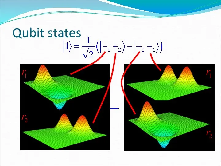
- 91. Qubit states
- 92. Qubit states
- 93. Realization of SWAP-gate
- 94. Realization of sqrt-SWAP
- 95. Realization of CNOT-gate
- 96. Coulomb blockade of current for measurement Dot occupied => potential barrier Dot vacant => potential well
- 97. Calculated transmission coefficients For fairly smooth potential profile the transmission through the well tends to 1
- 98. Альтернативные проекты QC во ФТИАН
- 99. Квантовый регистр на основе двойных квантовых точек в оптическом резонаторе
- 100. Квантовые компьютеры на NV-центрах в алмазе Искусственные алмазы: 3A2 Спиновый кубит на электронных уровнях NV-центра
- 101. Эпилог С Light at the end of the tunnel
- 102. Collaboration Наноэлектронные технологии АО Микрон и НИИМЭ ИФП СО РАН Фраунгоферовский институт (Германия) Графен Лаборатория двумерных
- 103. СПАСИБО за ВНИМАНИЕ!!!
- 104. THANK YOU !!!
- 108. Квантовые эффекты в полевых нанотранзисторах Уравнение Шредингера: Уравнение Пуассона: Формула Ландауэра:
- 109. Теория наноэлектронных приборов Цели современной наноэлектроники: Low-power и High-performance Альтернативные механизмы переноса тока: туннелирование Альтернативные материалы:
- 110. Транзисторы на основе графена: новые вопросы Объяснение отрицательной дифференциальной проводимости; Амбиполярные эффекты в полевых транзисторах –
- 111. Basic states in a DQD Potential in a DQD Symmetric Antisymmetric Electron wave-function in a DQD
- 112. Coulomb blockade for measurement
- 113. Терагерцовые лазеры на основе графена
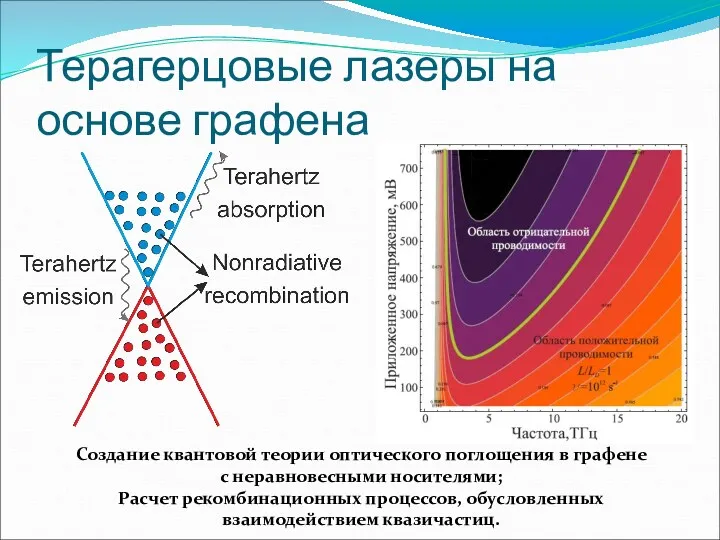
- 114. Терагерцовые лазеры на основе графена Создание квантовой теории оптического поглощения в графене с неравновесными носителями; Расчет
- 116. Скачать презентацию
План лекций
Технология наноэлектронных приборов
Теория наноэлектронных приборов
Квантовые компьютеры
План лекций
Технология наноэлектронных приборов
Теория наноэлектронных приборов
Квантовые компьютеры
Полевой транзистор – прибор с варьируемым сопротивлением
Полевой транзистор – прибор с варьируемым сопротивлением
The end of Moore’s ‘law’?
The end of Moore’s ‘law’?
IBM Gains Confidence in 22 nm ETSOI
(IEDM Conf., Dec. 2009)
IBM Gains Confidence in 22 nm ETSOI
(IEDM Conf., Dec. 2009)
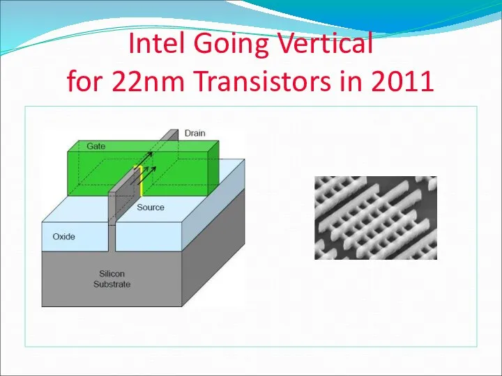
Intel Going Vertical
for 22nm Transistors in 2011
Intel Going Vertical
for 22nm Transistors in 2011
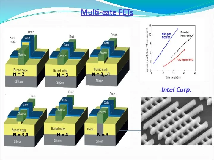
Multi-gate FETs
N = 2
N = 3
N = 3,14
N = 3,4
N =
Multi-gate FETs
N = 2
N = 3
N = 3,14
N = 3,4
N =
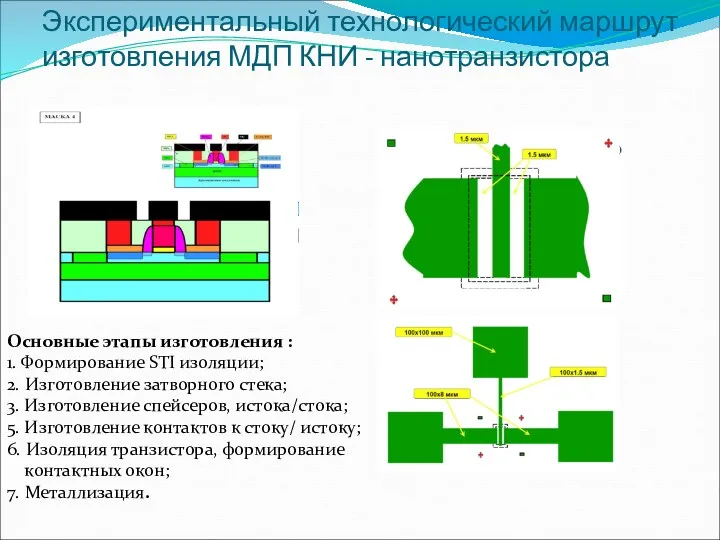
Экспериментальный технологический маршрут
изготовления МДП КНИ - нанотранзистора
Основные этапы изготовления :
1. Формирование
Экспериментальный технологический маршрут
изготовления МДП КНИ - нанотранзистора
Основные этапы изготовления :
1. Формирование
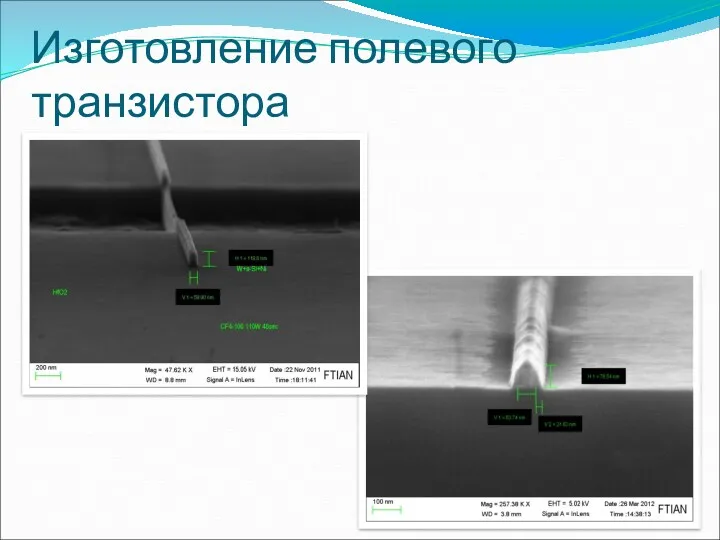
Изготовление полевого транзистора
Изготовление полевого транзистора
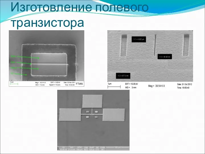
Изготовление полевого транзистора
Изготовление полевого транзистора
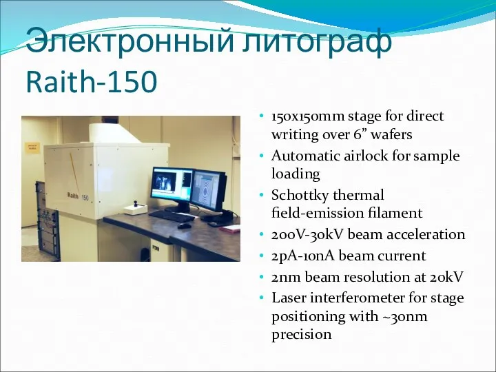
Электронный литограф
Raith-150
150x150mm stage for direct writing over 6” wafers
Automatic airlock
Электронный литограф
Raith-150
150x150mm stage for direct writing over 6” wafers
Automatic airlock
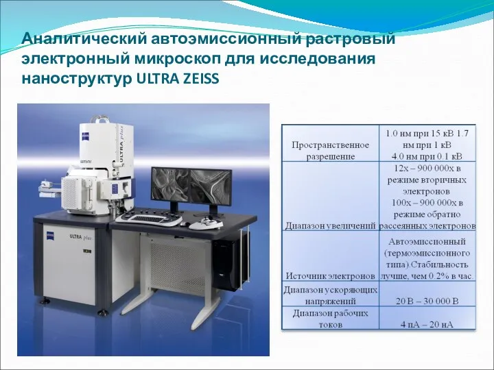
Аналитический автоэмиссионный растровый электронный микроскоп для исследования наноструктур ULTRA ZEISS
Аналитический автоэмиссионный растровый электронный микроскоп для исследования наноструктур ULTRA ZEISS
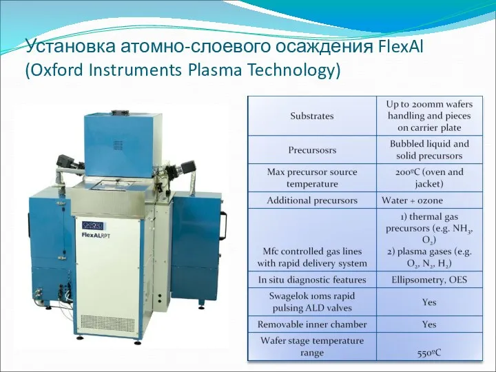
Установка атомно-слоевого осаждения FlexAl (Oxford Instruments Plasma Technology)
Установка атомно-слоевого осаждения FlexAl (Oxford Instruments Plasma Technology)
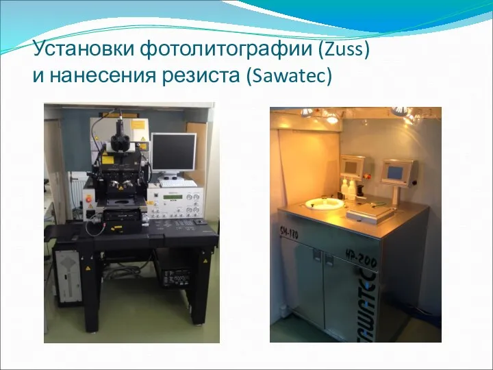
Установки фотолитографии (Zuss)
и нанесения резиста (Sawatec)
Установки фотолитографии (Zuss)
и нанесения резиста (Sawatec)
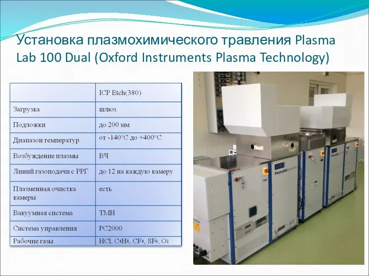
Установка плазмохимического травления Plasma Lab 100 Dual (Oxford Instruments Plasma Technology)
Установка плазмохимического травления Plasma Lab 100 Dual (Oxford Instruments Plasma Technology)
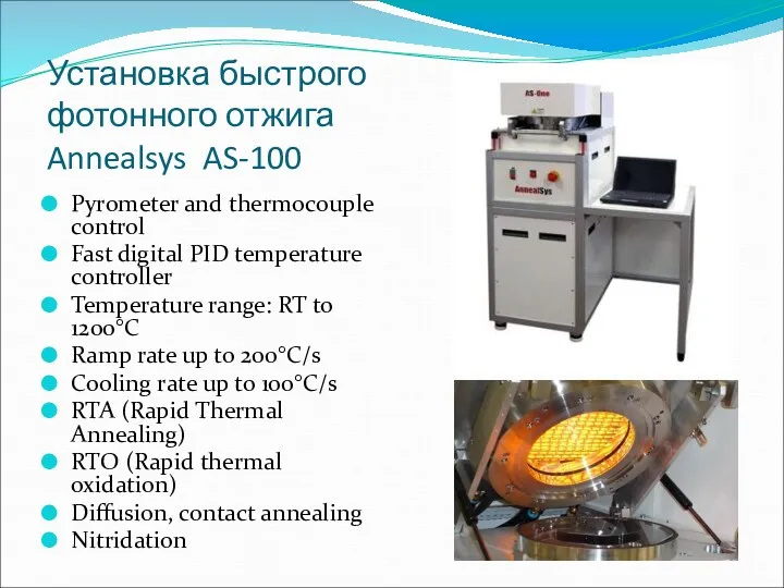
Установка быстрого фотонного отжига
Annealsys AS-100
Pyrometer and thermocouple control
Fast digital PID
Установка быстрого фотонного отжига
Annealsys AS-100
Pyrometer and thermocouple control
Fast digital PID
Теория наноэлектронных приборов
Требования современной электроники: Low-power и High-performance
Альтернативные механизмы переноса тока:
Теория наноэлектронных приборов
Требования современной электроники: Low-power и High-performance
Альтернативные механизмы переноса тока:
SIMULATION
SIMULATION
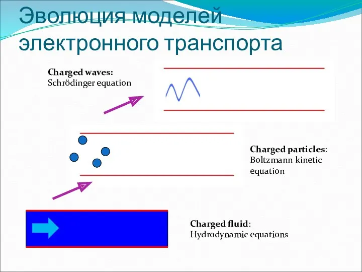
Эволюция моделей электронного транспорта
Charged fluid:
Hydrodynamic equations
Charged particles:
Boltzmann kinetic equation
Charged waves:
Schrödinger equation
Эволюция моделей электронного транспорта
Charged fluid:
Hydrodynamic equations
Charged particles:
Boltzmann kinetic equation
Charged waves:
Schrödinger equation
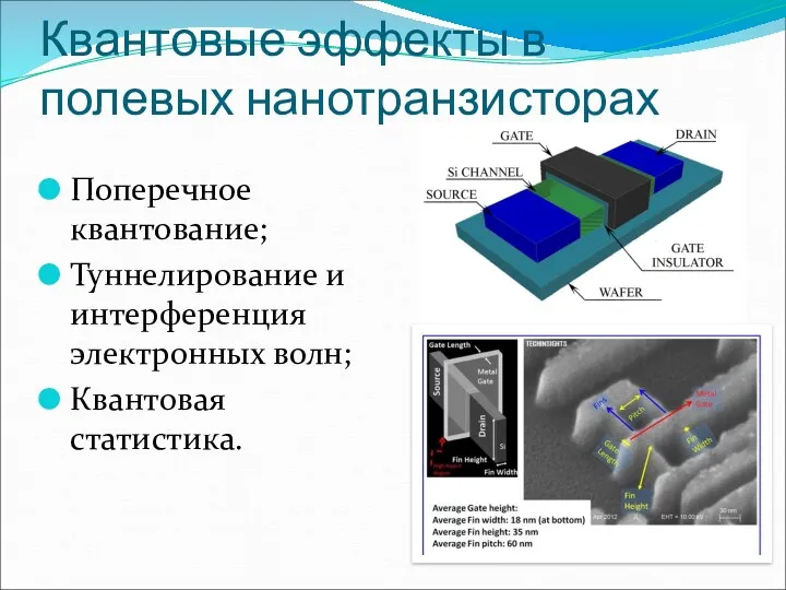
Квантовые эффекты в полевых нанотранзисторах
Поперечное квантование;
Туннелирование и интерференция электронных волн;
Квантовая статистика.
Квантовые эффекты в полевых нанотранзисторах
Поперечное квантование;
Туннелирование и интерференция электронных волн;
Квантовая статистика.
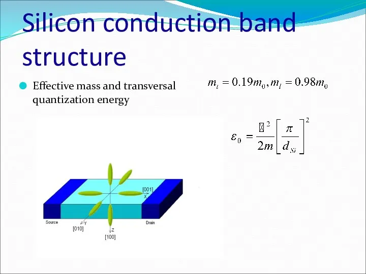
Silicon conduction band structure
Effective mass and transversal quantization energy
Silicon conduction band structure
Effective mass and transversal quantization energy
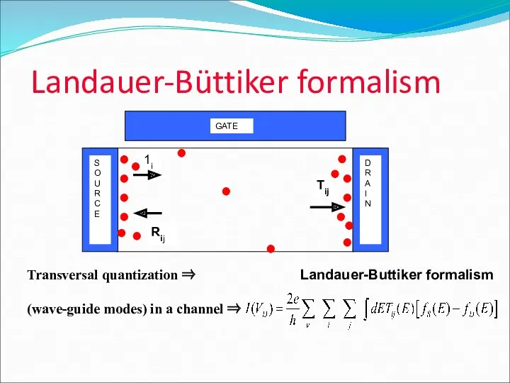
Landauer-Büttiker formalism
Transversal quantization ⇒
(wave-guide modes) in a channel ⇒
Landauer-Buttiker
Landauer-Büttiker formalism
Transversal quantization ⇒
(wave-guide modes) in a channel ⇒
Landauer-Buttiker
Everlasting controversy in kinetic simulation
Distribution function (equilibrium) is known only in
Everlasting controversy in kinetic simulation
Distribution function (equilibrium) is known only in
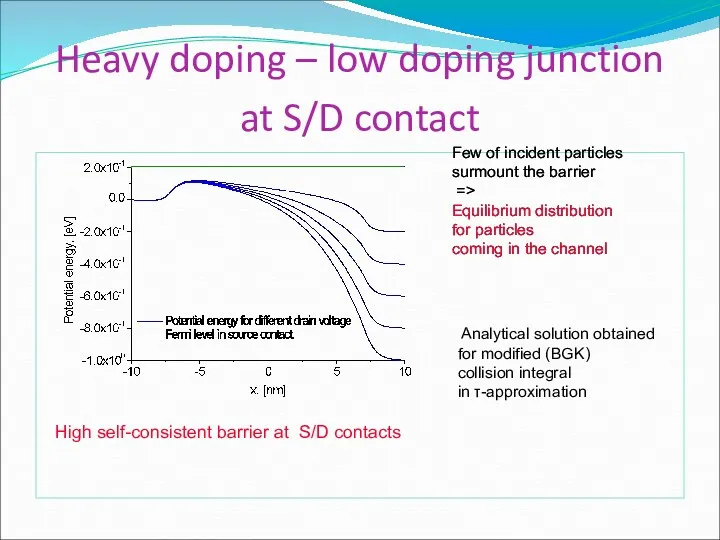
Heavy doping – low doping junction
at S/D contact
High self-consistent
Heavy doping – low doping junction
at S/D contact
High self-consistent
Main strategy of simulation
Self-consistent solution of
Schrödinger equation
+
Maxwell equation
Main strategy of simulation
Self-consistent solution of
Schrödinger equation
+
Maxwell equation
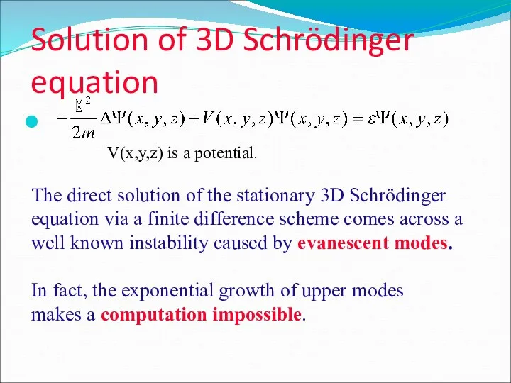
Solution of 3D Schrödinger equation
V(x,y,z) is a potential.
The direct solution
Solution of 3D Schrödinger equation
V(x,y,z) is a potential.
The direct solution
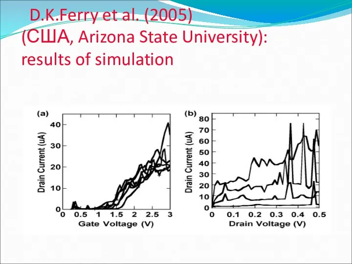
D.K.Ferry et al. (2005)
(США, Arizona State University):
results of simulation
D.K.Ferry et al. (2005)
(США, Arizona State University):
results of simulation
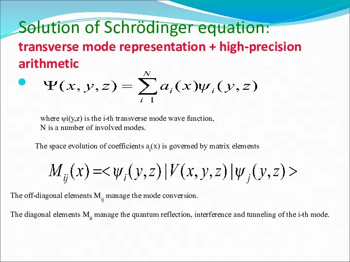
Solution of Schrödinger equation:
transverse mode representation + high-precision arithmetic
where
Solution of Schrödinger equation:
transverse mode representation + high-precision arithmetic
where
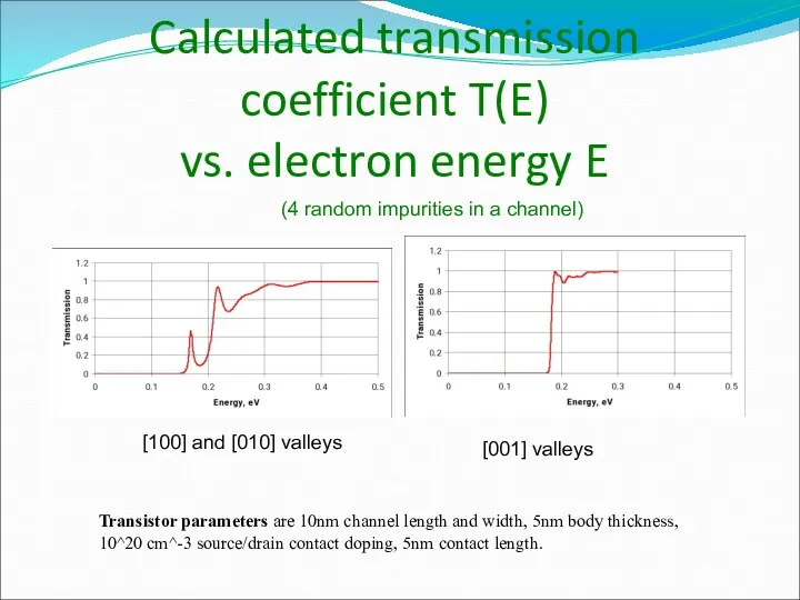
Calculated transmission coefficient T(E)
vs. electron energy E
Transistor parameters are 10nm
Calculated transmission coefficient T(E)
vs. electron energy E
Transistor parameters are 10nm
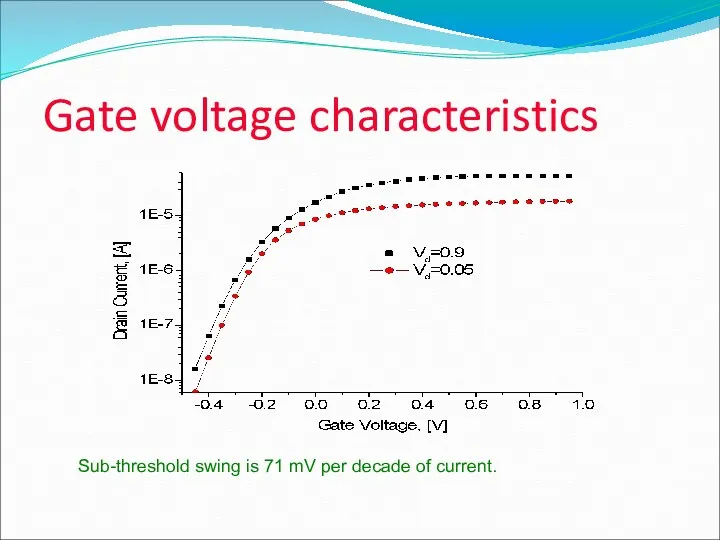
Gate voltage characteristics
Sub-threshold swing is 71 mV per decade of current.
Gate voltage characteristics
Sub-threshold swing is 71 mV per decade of current.
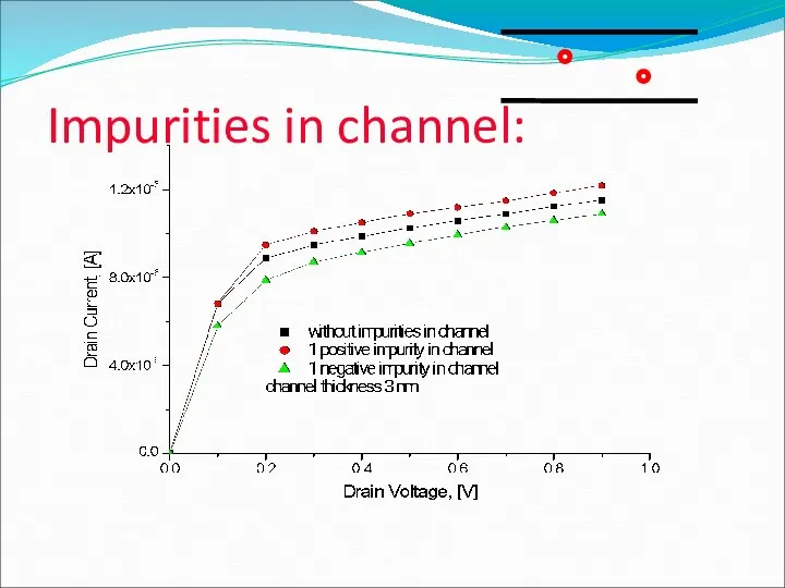
Impurities in channel:
Impurities in channel:
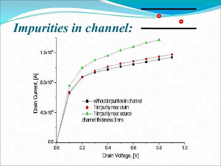
Impurities in channel:
Impurities in channel:
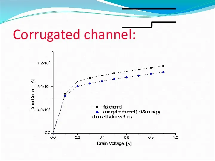
Corrugated channel:
Corrugated channel:
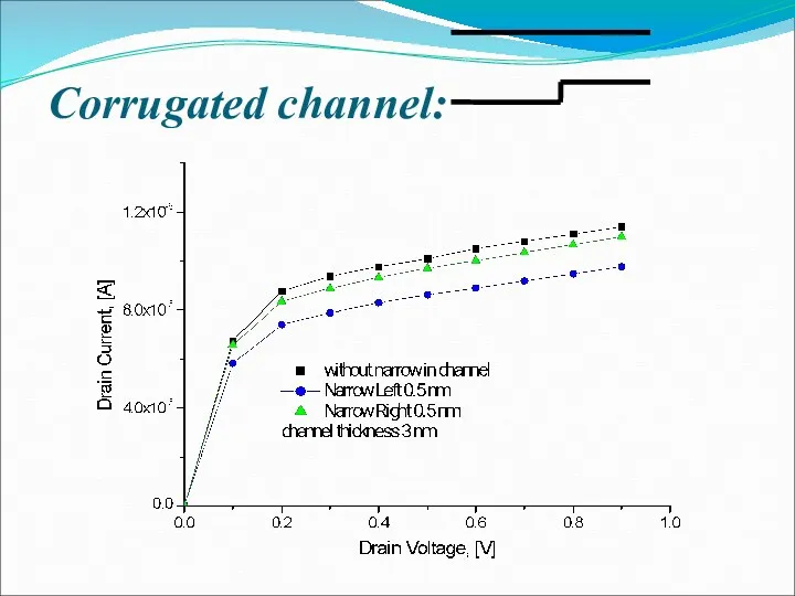
Corrugated channel:
Corrugated channel:
Dispersion of characteristics
5-15% in calculated I-V curves
< 10% is an everlasting
Dispersion of characteristics
5-15% in calculated I-V curves
< 10% is an everlasting
Требования к современной электронике
Требования к современной электронике
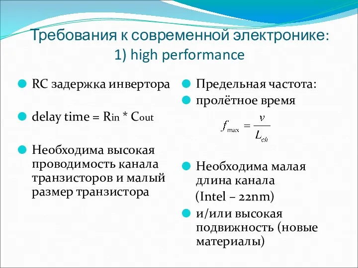
Требования к современной электронике:
1) high performance
RC задержка инвертора
delay time = Rin
Требования к современной электронике:
1) high performance
RC задержка инвертора
delay time = Rin
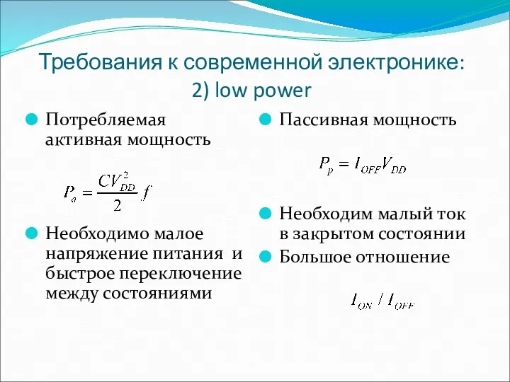
Требования к современной электронике:
2) low power
Потребляемая активная мощность
Необходимо малое напряжение питания
Требования к современной электронике:
2) low power
Потребляемая активная мощность
Необходимо малое напряжение питания
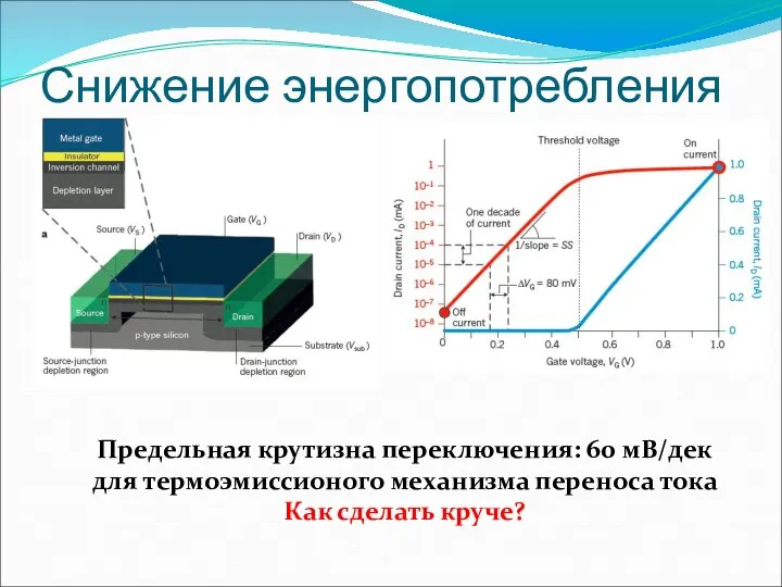
Снижение энергопотребления
Предельная крутизна переключения: 60 мВ/дек
для термоэмиссионого механизма переноса тока
Как сделать
Снижение энергопотребления
Предельная крутизна переключения: 60 мВ/дек
для термоэмиссионого механизма переноса тока
Как сделать
Туннельные транзисторы
позволяют достичь
подпороговой крутизны выше (60мВ/дек)-1
при комнатной температуре
Туннельные транзисторы
позволяют достичь
подпороговой крутизны выше (60мВ/дек)-1
при комнатной температуре
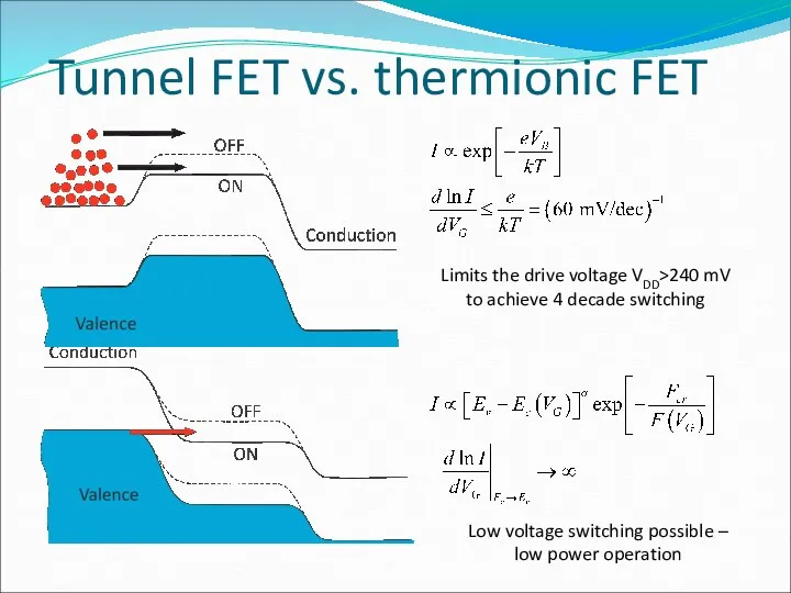
Tunnel FET vs. thermionic FET
Limits the drive voltage VDD>240 mV
to achieve
Tunnel FET vs. thermionic FET
Limits the drive voltage VDD>240 mV
to achieve
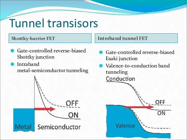
Tunnel transisors
Shottky-barrier FET
Interband tunnel FET
Gate-controlled reverse-biased Shottky junction
Intraband metal-semiconductor tunneling
Gate-controlled reverse-biased
Tunnel transisors
Shottky-barrier FET
Interband tunnel FET
Gate-controlled reverse-biased Shottky junction
Intraband metal-semiconductor tunneling
Gate-controlled reverse-biased
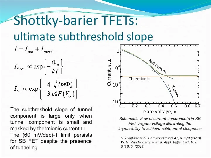
Shottky-barier TFETs:
ultimate subthreshold slope
The subthreshold slope of tunnel component is
Shottky-barier TFETs:
ultimate subthreshold slope
The subthreshold slope of tunnel component is
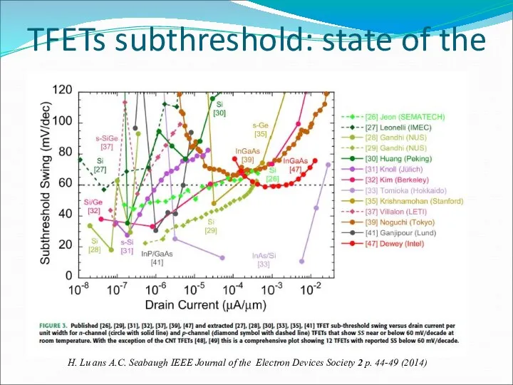
TFETs subthreshold: state of the art
H. Lu ans A.C. Seabaugh IEEE
TFETs subthreshold: state of the art
H. Lu ans A.C. Seabaugh IEEE
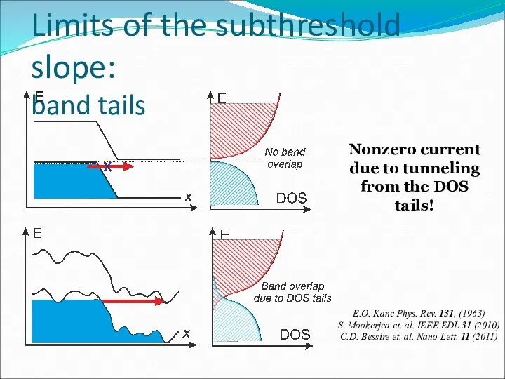
Limits of the subthreshold slope:
band tails
Nonzero current due to tunneling from
Limits of the subthreshold slope:
band tails
Nonzero current due to tunneling from
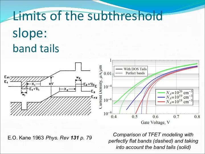
E.O. Kane 1963 Phys. Rev 131 p. 79
Comparison of TFET modeling
E.O. Kane 1963 Phys. Rev 131 p. 79
Comparison of TFET modeling
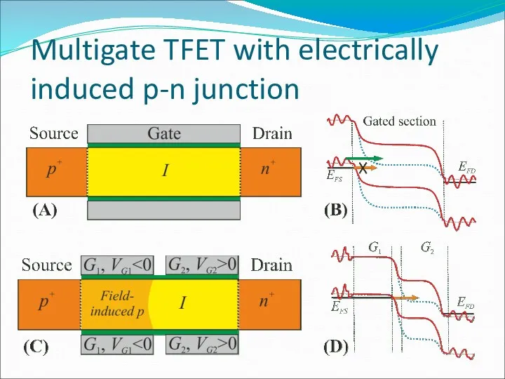
Multigate TFET with electrically induced p-n junction
Multigate TFET with electrically induced p-n junction

Simulated characteristics of MG-TFET
Simulated I(VG)-curve for multigate FET with electrically induced
Simulated characteristics of MG-TFET
Simulated I(VG)-curve for multigate FET with electrically induced
Graphene FETs
Graphene FETs
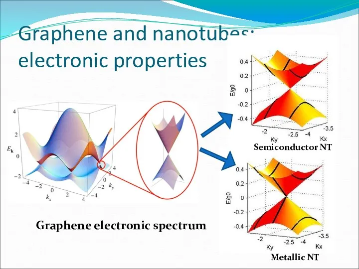
Graphene and nanotubes:
electronic properties
Graphene electronic spectrum
Semiconductor NT
Metallic NT
Graphene and nanotubes:
electronic properties
Graphene electronic spectrum
Semiconductor NT
Metallic NT
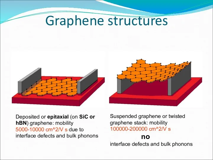
Graphene structures
Deposited or epitaxial (on SiC or hBN) graphene: mobility 5000-10000
Graphene structures
Deposited or epitaxial (on SiC or hBN) graphene: mobility 5000-10000
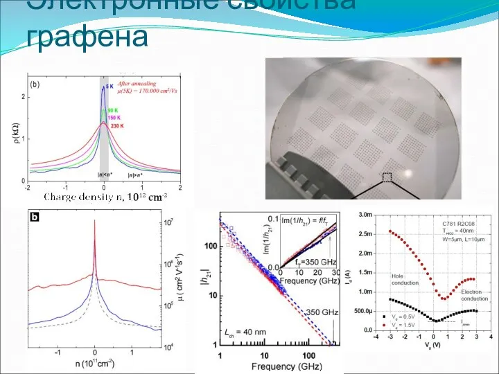
Электронные свойства графена
Электронные свойства графена
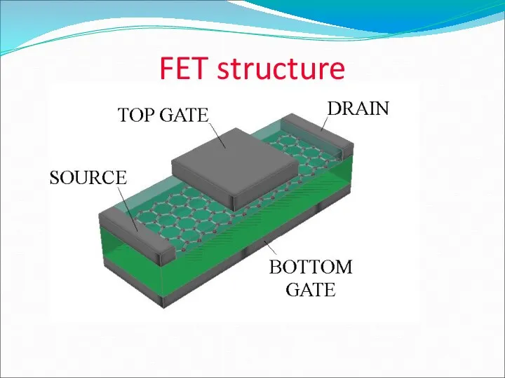
FET structure
FET structure
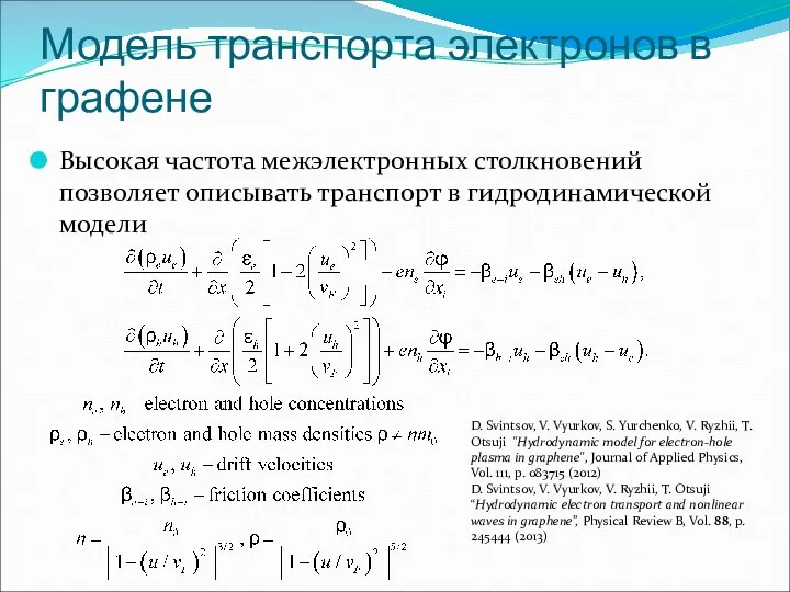
Модель транспорта электронов в графене
Высокая частота межэлектронных столкновений позволяет описывать транспорт
Модель транспорта электронов в графене
Высокая частота межэлектронных столкновений позволяет описывать транспорт
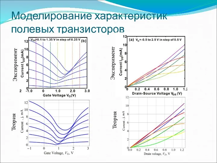
Моделирование характеристик полевых транзисторов
Эксперимент
Эксперимент
Теория
Теория
Моделирование характеристик полевых транзисторов
Эксперимент
Эксперимент
Теория
Теория
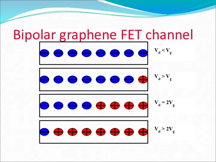
Bipolar graphene FET channel
Bipolar graphene FET channel
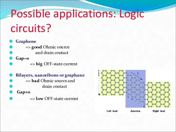
Possible applications: Logic circuits?
Graphene
=> good Ohmic source
and drain contact
Gap=0
Possible applications: Logic circuits?
Graphene
=> good Ohmic source
and drain contact
Gap=0
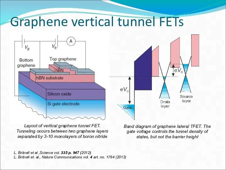
Graphene vertical tunnel FETs
L. Britnell et al ,Science vol. 335 p.
Graphene vertical tunnel FETs
L. Britnell et al ,Science vol. 335 p.
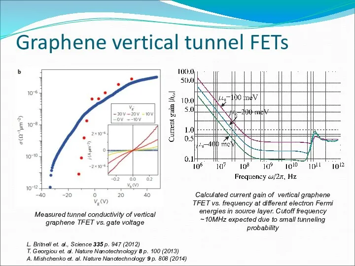
Graphene vertical tunnel FETs
L. Britnell et. al., Science 335 p. 947
Graphene vertical tunnel FETs
L. Britnell et. al., Science 335 p. 947
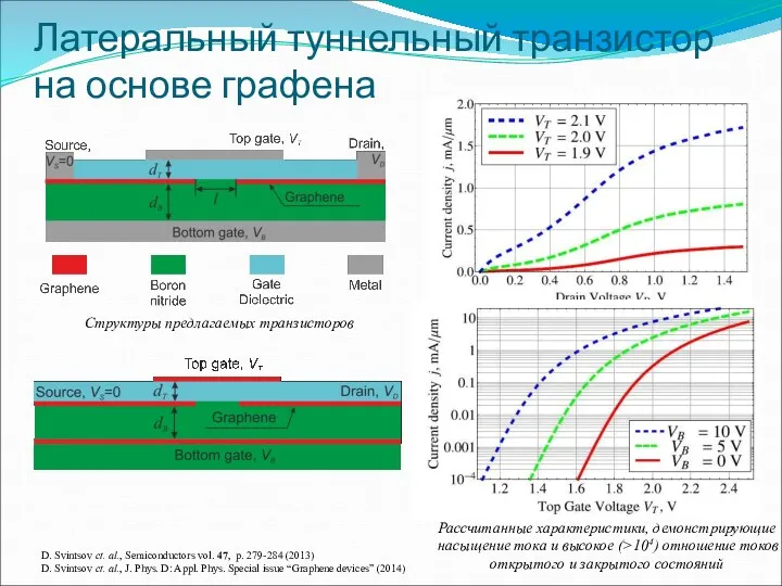
Латеральный туннельный транзистор на основе графена
D. Svintsov et. al., Semiconductors vol.
Латеральный туннельный транзистор на основе графена
D. Svintsov et. al., Semiconductors vol.
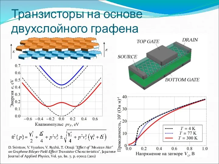
Транзисторы на основе двухслойного графена
D. Svintsov, V. Vyurkov, V. Ryzhii, T.
Транзисторы на основе двухслойного графена
D. Svintsov, V. Vyurkov, V. Ryzhii, T.
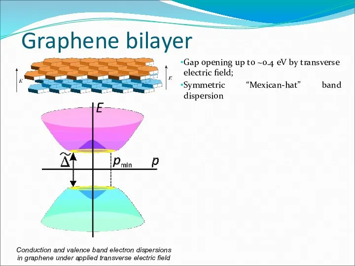
Graphene bilayer
Conduction and valence band electron dispersions in graphene under applied
Graphene bilayer
Conduction and valence band electron dispersions in graphene under applied
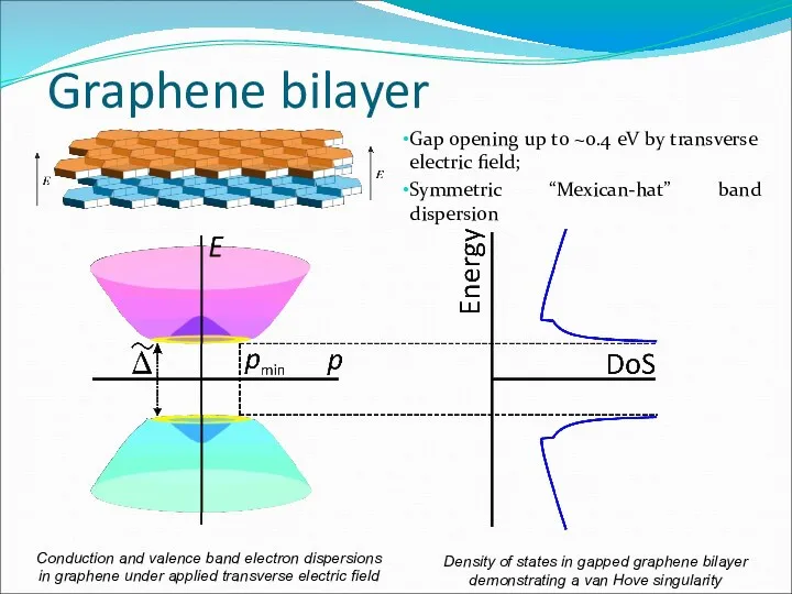
Graphene bilayer
Conduction and valence band electron dispersions in graphene under applied
Graphene bilayer
Conduction and valence band electron dispersions in graphene under applied
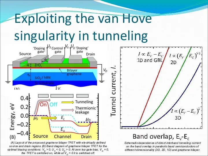
Exploiting the van Hove singularity in tunneling
(A) Layout of the proposed
Exploiting the van Hove singularity in tunneling
(A) Layout of the proposed
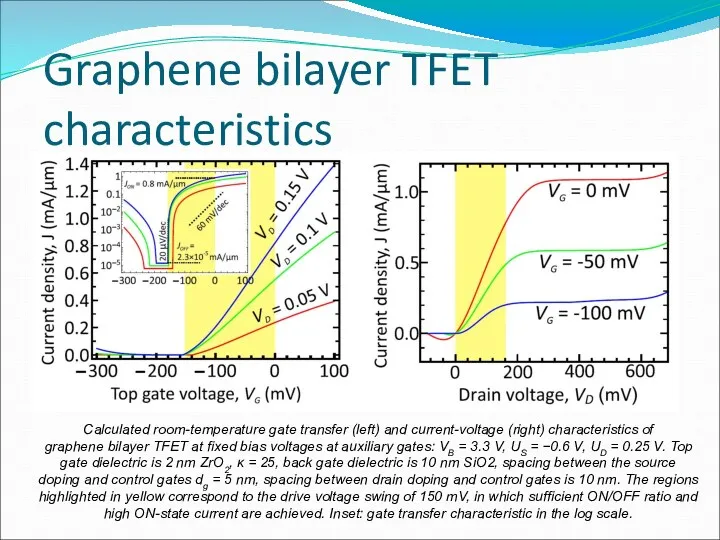
Graphene bilayer TFET characteristics
Calculated room-temperature gate transfer (left) and current-voltage (right)
Graphene bilayer TFET characteristics
Calculated room-temperature gate transfer (left) and current-voltage (right)
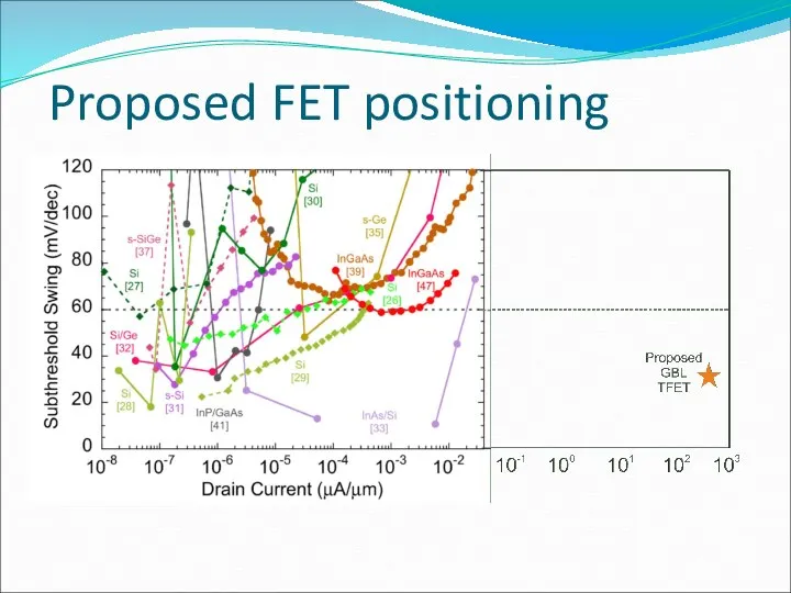
Proposed FET positioning
Proposed FET positioning
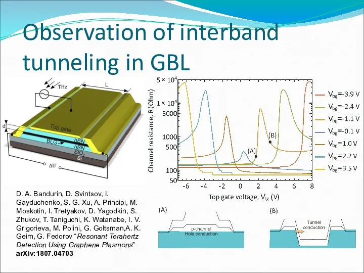
Observation of interband tunneling in GBL
D. A. Bandurin, D. Svintsov, I. Gayduchenko, S. G.
Observation of interband tunneling in GBL
D. A. Bandurin, D. Svintsov, I. Gayduchenko, S. G.
QUANTUM COMPUTERS
QUANTUM COMPUTERS
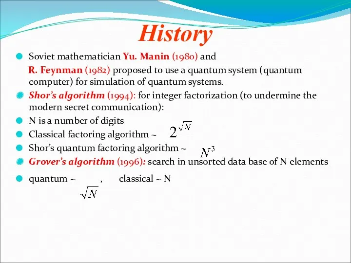
History
Soviet mathematician Yu. Manin (1980) and
R. Feynman (1982) proposed
History
Soviet mathematician Yu. Manin (1980) and
R. Feynman (1982) proposed
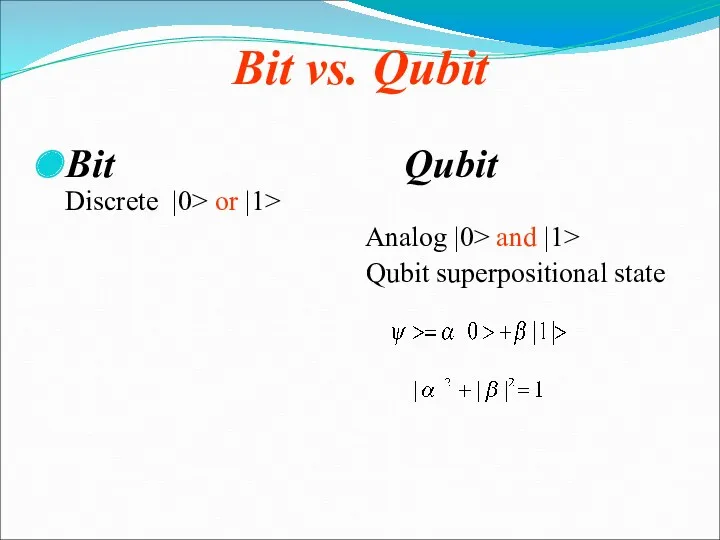
Bit vs. Qubit
Bit Qubit Discrete |0> or |1>
Analog |0>
Bit vs. Qubit
Bit Qubit Discrete |0> or |1>
Analog |0>
Classical register vs. Quantum register
Bits Qubits
Classical register Quantum register
Classical register vs. Quantum register
Bits Qubits
Classical register Quantum register
Entangled states in quantum computer: quantum parallelism
Entangled states in quantum computer: quantum parallelism
Realism and locality
in quantum mechanics
Realism and locality
in quantum mechanics
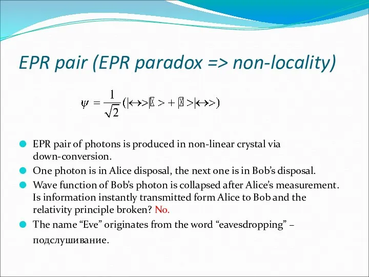
EPR pair (EPR paradox => non-locality)
EPR pair of photons is
EPR pair (EPR paradox => non-locality)
EPR pair of photons is
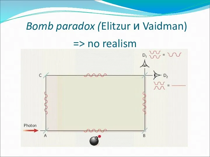
Bomb paradox (Elitzur и Vaidman)
=> no realism
Bomb paradox (Elitzur и Vaidman)
=> no realism
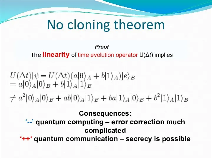
No cloning theorem
Consequences:
‘--’ quantum computing – error correction much
No cloning theorem
Consequences:
‘--’ quantum computing – error correction much
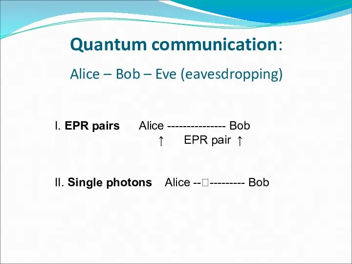
Quantum communication:
Alice – Bob – Eve (eavesdropping)
I. EPR pairs
Quantum communication:
Alice – Bob – Eve (eavesdropping)
I. EPR pairs
Realizations
of quantum computers
Dopant atoms in silicon
Quantum dots
Ions in traps
Cold atoms
Realizations
of quantum computers
Dopant atoms in silicon
Quantum dots
Ions in traps
Cold atoms
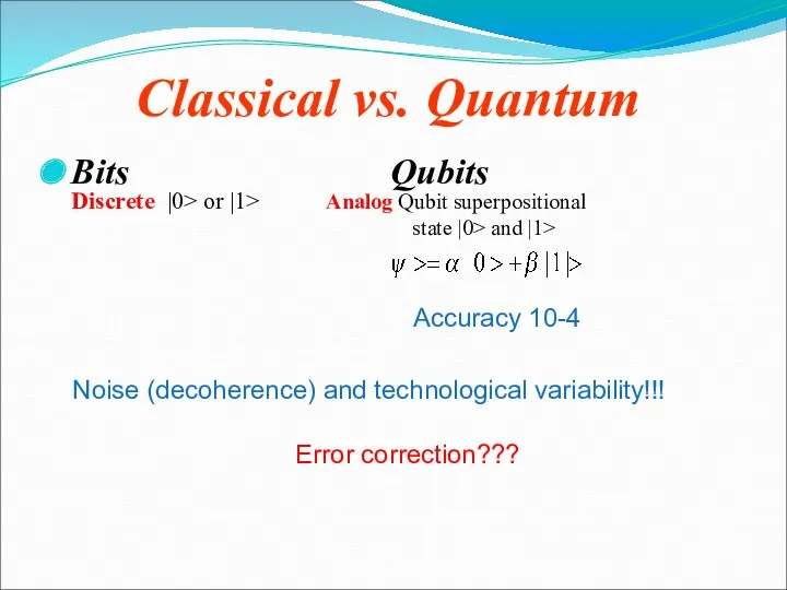
Classical vs. Quantum
Bits Qubits Discrete |0> or |1> Analog Qubit superpositional
Classical vs. Quantum
Bits Qubits Discrete |0> or |1> Analog Qubit superpositional
Classical vs. quantum
Classical vs. quantum
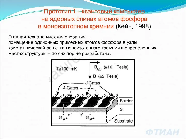
ФТИАН
Прототип 1 - квантовый компьютер
на ядерных спинах атомов фосфора
в моноизотопном
ФТИАН
Прототип 1 - квантовый компьютер
на ядерных спинах атомов фосфора
в моноизотопном
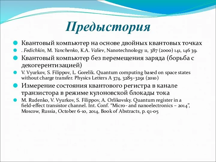
Предыстория
Квантовый компьютер на основе двойных квантовых точках
. Fedichkin, M. Yanchenko, K.A.
Предыстория
Квантовый компьютер на основе двойных квантовых точках
. Fedichkin, M. Yanchenko, K.A.
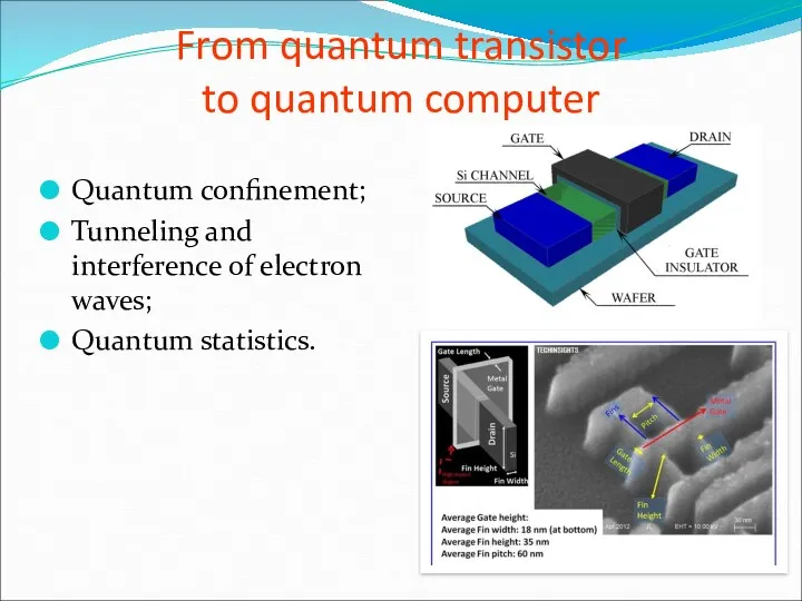
From quantum transistor
to quantum computer
Quantum confinement;
Tunneling and interference of electron
From quantum transistor
to quantum computer
Quantum confinement;
Tunneling and interference of electron
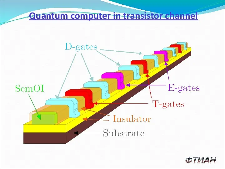
Quantum computer in transistor channel
ФТИАН
Quantum computer in transistor channel
ФТИАН
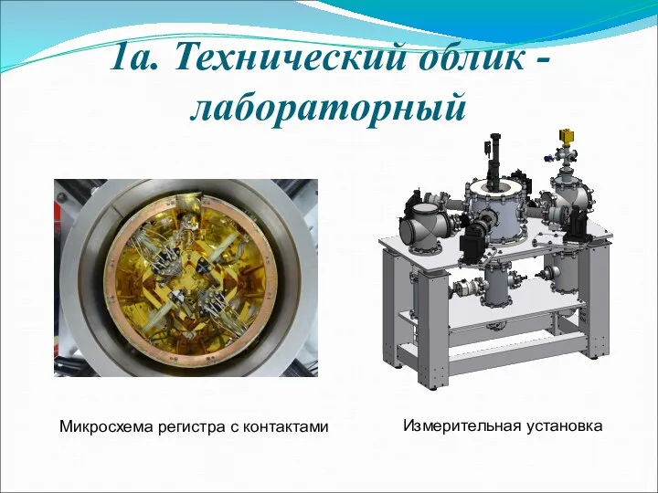
1а. Технический облик - лабораторный
Микросхема регистра с контактами
Измерительная установка
1а. Технический облик - лабораторный
Микросхема регистра с контактами
Измерительная установка
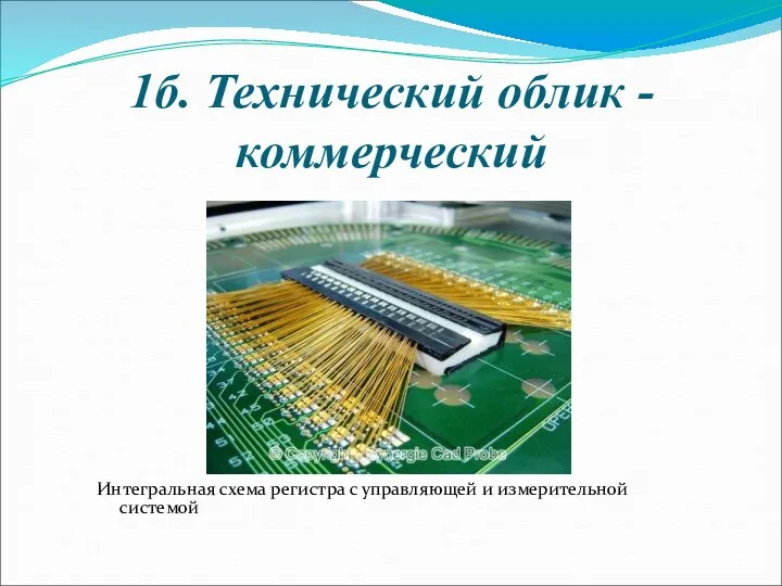
1б. Технический облик - коммерческий
Интегральная схема регистра с управляющей и измерительной
1б. Технический облик - коммерческий
Интегральная схема регистра с управляющей и измерительной
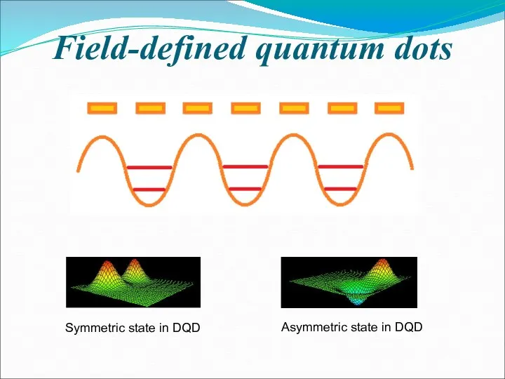
Field-defined quantum dots
Symmetric state in DQD
Asymmetric state in DQD
Field-defined quantum dots
Symmetric state in DQD
Asymmetric state in DQD
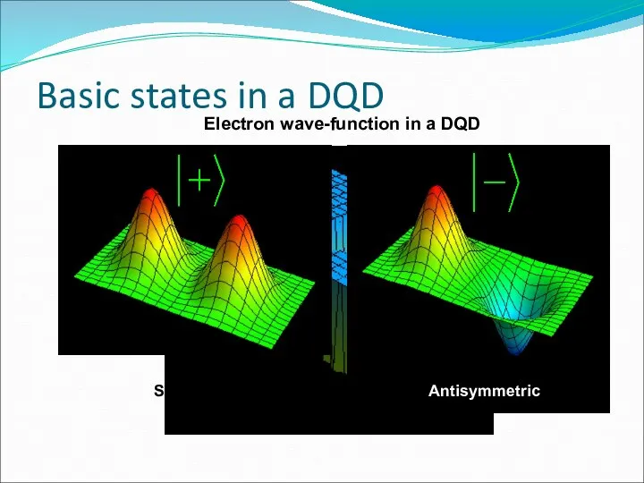
Basic states in a DQD
Potential in a DQD
Symmetric
Antisymmetric
Electron wave-function in a
Basic states in a DQD
Potential in a DQD
Symmetric
Antisymmetric
Electron wave-function in a
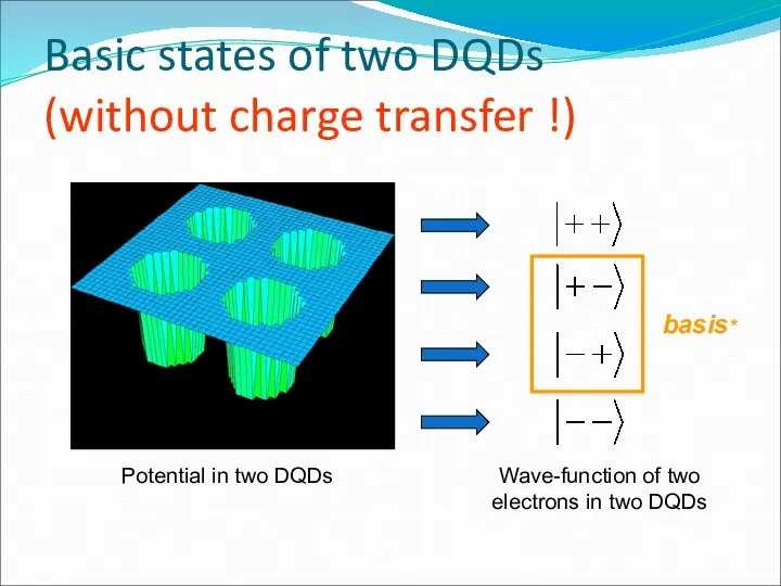
Basic states of two DQDs
(without charge transfer !)
Potential in two
Basic states of two DQDs
(without charge transfer !)
Potential in two
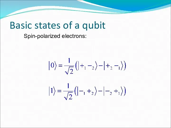
Basic states of a qubit
Spin-polarized electrons:
Basic states of a qubit
Spin-polarized electrons:
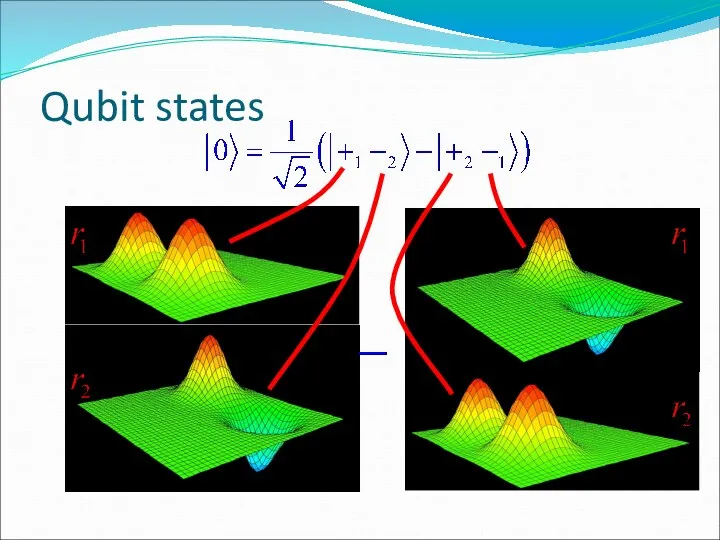
Qubit states
Qubit states
Qubit states
Qubit states
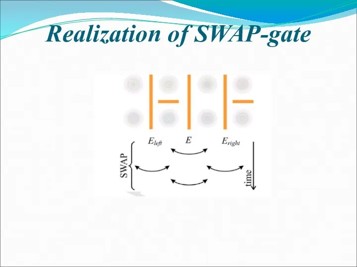
Realization of SWAP-gate
Realization of SWAP-gate
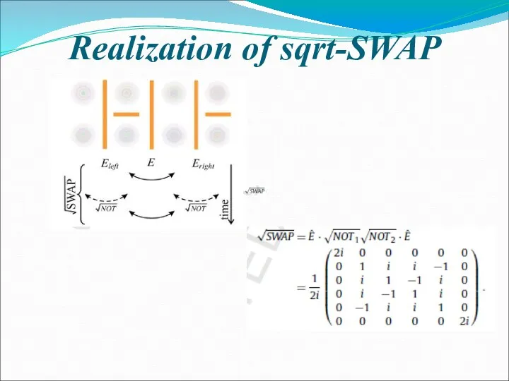
Realization of sqrt-SWAP
Realization of sqrt-SWAP
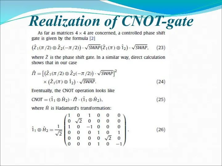
Realization of CNOT-gate
Realization of CNOT-gate
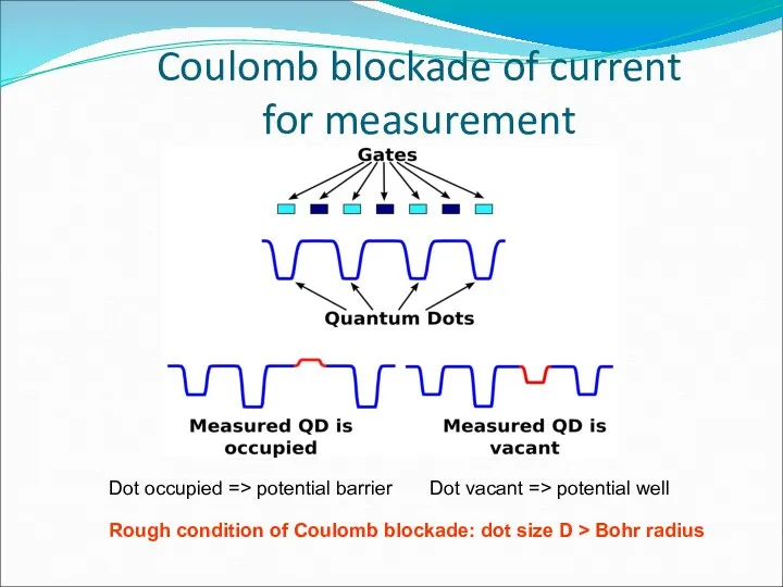
Coulomb blockade of current
for measurement
Dot occupied => potential barrier
Dot vacant
Coulomb blockade of current
for measurement
Dot occupied => potential barrier
Dot vacant
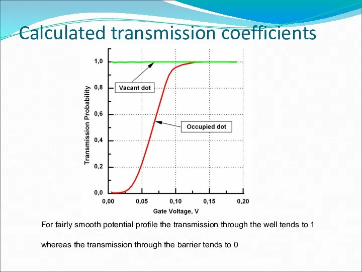
Calculated transmission coefficients
For fairly smooth potential profile the transmission through the
Calculated transmission coefficients
For fairly smooth potential profile the transmission through the
Альтернативные проекты QC
во ФТИАН
Альтернативные проекты QC
во ФТИАН
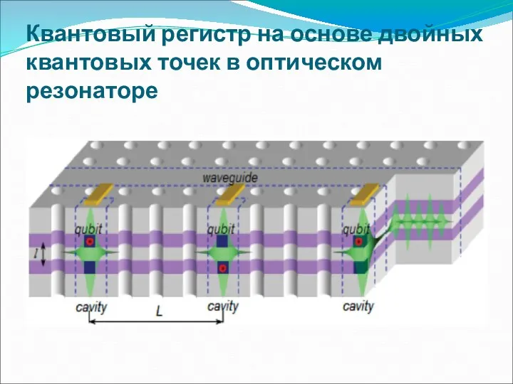
Квантовый регистр на основе двойных квантовых точек в оптическом резонаторе
Квантовый регистр на основе двойных квантовых точек в оптическом резонаторе
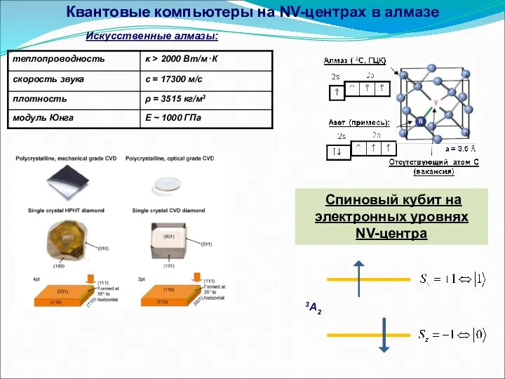
Квантовые компьютеры на NV-центрах в алмазе
Искусственные алмазы:
3A2
Спиновый кубит на электронных
Квантовые компьютеры на NV-центрах в алмазе
Искусственные алмазы:
3A2
Спиновый кубит на электронных
Эпилог
С
Light at the end of the tunnel
Эпилог
С
Light at the end of the tunnel
Collaboration
Наноэлектронные технологии
АО Микрон и НИИМЭ
ИФП СО РАН
Фраунгоферовский институт (Германия)
Графен
Лаборатория двумерных систем
Collaboration
Наноэлектронные технологии
АО Микрон и НИИМЭ
ИФП СО РАН
Фраунгоферовский институт (Германия)
Графен
Лаборатория двумерных систем
СПАСИБО за ВНИМАНИЕ!!!
СПАСИБО за ВНИМАНИЕ!!!

THANK YOU !!!
THANK YOU !!!


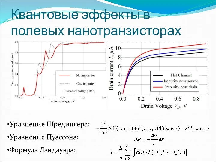
Квантовые эффекты в полевых нанотранзисторах
Уравнение Шредингера:
Уравнение Пуассона:
Формула Ландауэра:
Квантовые эффекты в полевых нанотранзисторах
Уравнение Шредингера:
Уравнение Пуассона:
Формула Ландауэра:
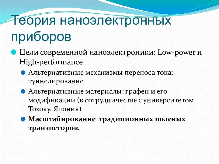
Теория наноэлектронных приборов
Цели современной наноэлектроники: Low-power и High-performance
Альтернативные механизмы переноса тока:
Теория наноэлектронных приборов
Цели современной наноэлектроники: Low-power и High-performance
Альтернативные механизмы переноса тока:
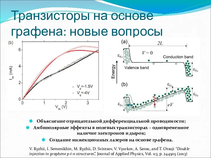
Транзисторы на основе графена: новые вопросы
Объяснение отрицательной дифференциальной проводимости;
Амбиполярные эффекты в
Транзисторы на основе графена: новые вопросы
Объяснение отрицательной дифференциальной проводимости;
Амбиполярные эффекты в

Basic states in a DQD
Potential in a DQD
Symmetric
Antisymmetric
Electron wave-function in a
Basic states in a DQD
Potential in a DQD
Symmetric
Antisymmetric
Electron wave-function in a
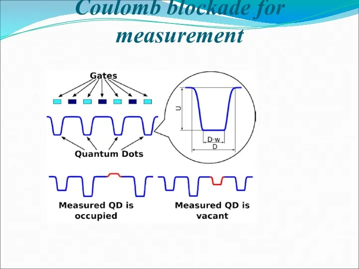
Coulomb blockade for measurement
Coulomb blockade for measurement
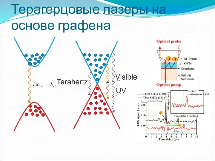
Терагерцовые лазеры на основе графена
Терагерцовые лазеры на основе графена
Терагерцовые лазеры на основе графена
Создание квантовой теории оптического поглощения в графене
Терагерцовые лазеры на основе графена
Создание квантовой теории оптического поглощения в графене
 Бронхиальная астма у детей
 Человек и среда обитания. Природные опасности
 Клинический случай Левамизолиндуцированная лейкоэнфефалопатия
 Атмосфера. Всероссийский конкурс
 Конструкционные материалы, применяемые при проектировании объектов топливно-энергетического комплекса
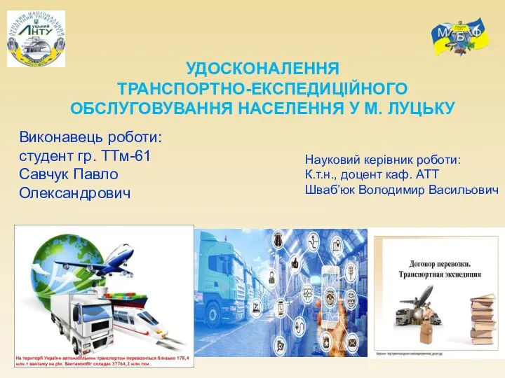 Удосконалення транспортно-експедиційного обслуговування населення у місті Луцьку
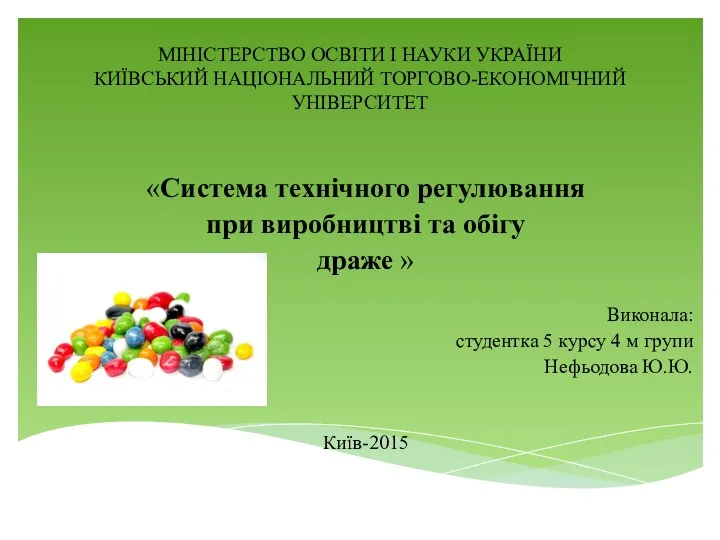 Система технічного регулювання при виробництві та обігу драже
 Кроссворд Профессии.
 Электронная игра Подбери по форме и цвету
 Как сделать эффективную презентацию?
 Сто лет учительской династии
 23 февраля
 Аналіз мас-спектрів
 Использование социальной сети ВКонтакте для совершенствования учебно-воспитательного процесса
 Geolika. Проект планировки территории планировочного района юго-восточной части г. Долинска
 Гуманизм: абстрактный или классовый, по роману А.А. Фадеева Разгром
 Техника описания различных легко-атлетических движений
 Основные принципы ФГОС ДО
 Получение азотной кислоты
 Презентация Пасха
 Стандарты информационной безопасности: Общие критерии
 Политический кризис Речи Посполитой
 Родительское собрание 5 класс
 Процесс постановки биотехнологической продукции на производство
 Размножение растений
 Гайд по девушке для задрота
 Симптомы и синдромы при заболеваниях печени
 Ощущения у детей с нарушением речи