- Seminar on kesterites

Содержание
- 2. Outline Motivation Basic properties Crystal structure and phases Defects/Doping Solar cells Limiting factors Laboratory for Thin
- 3. Motivation High efficient chalcogen based technologies rely on elements which are rare or costly (e.g. In,
- 4. Material properties Laboratory for Thin Films and Photovoltaics 1Chen et al., Crystal and electronic band structure
- 5. Crystal structure Laboratory for Thin Films and Photovoltaics S. Chen, X. G. Gong, A. Walsh, S-H
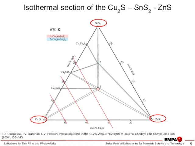
- 6. Isothermal section of the Cu2S – SnS2 - ZnS Laboratory for Thin Films and Photovoltaics I.D.
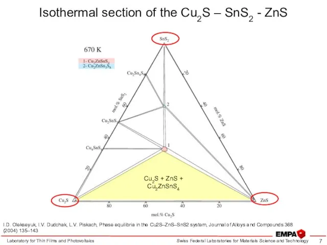
- 7. Isothermal section of the Cu2S – SnS2 - ZnS Laboratory for Thin Films and Photovoltaics I.D.
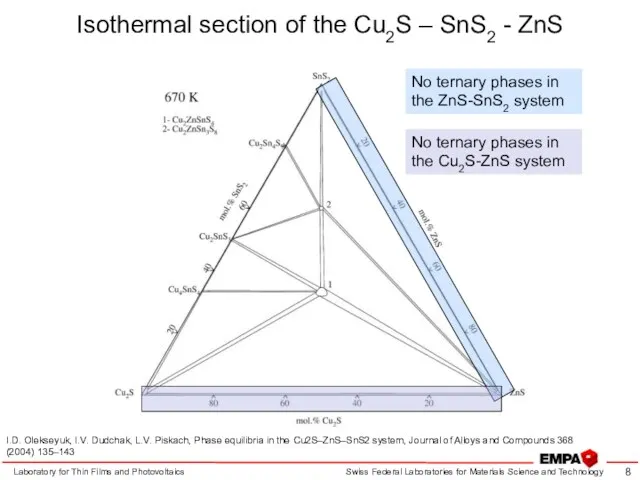
- 8. Isothermal section of the Cu2S – SnS2 - ZnS Laboratory for Thin Films and Photovoltaics I.D.
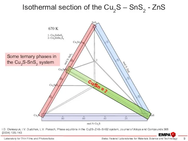
- 9. Isothermal section of the Cu2S – SnS2 - ZnS Laboratory for Thin Films and Photovoltaics I.D.
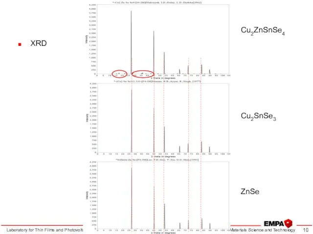
- 10. Kesterite characterization Laboratory for Thin Films and Photovoltaics XRD Cu2ZnSnSe4 Cu2SnSe3 ZnSe
- 11. Kesterite characterization XRD Laboratory for Thin Films and Photovoltaics hydrazine processed CZTSSe David B. Mitzi, Oki
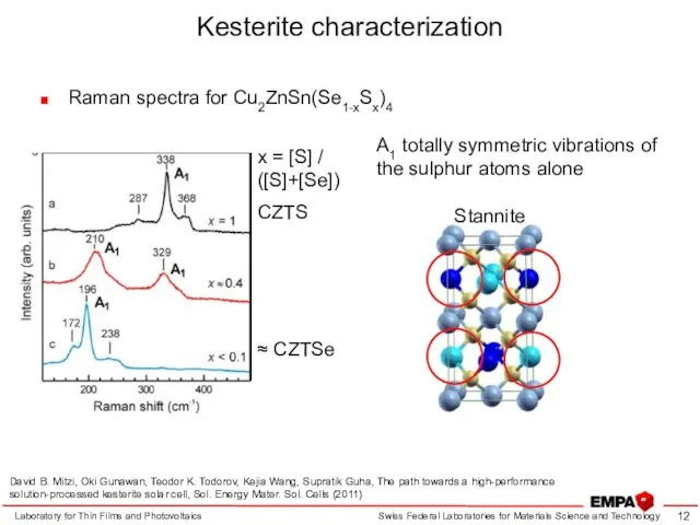
- 12. Kesterite characterization Raman spectra for Cu2ZnSn(Se1-xSx)4 Laboratory for Thin Films and Photovoltaics Stannite x = [S]
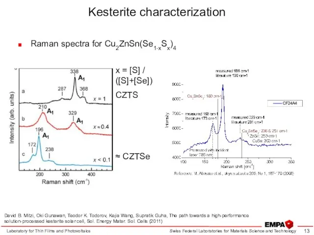
- 13. Kesterite characterization Raman spectra for Cu2ZnSn(Se1-xSx)4 Laboratory for Thin Films and Photovoltaics x = [S] /
- 14. Electrical properties Laboratory for Thin Films and Photovoltaics 1 W. K. Metzger et al., Recombination kinetics
- 15. Intrinsic defects Laboratory for Thin Films and Photovoltaics 1 Chen et al., Intrinsic point defects and
- 16. Defect complexes Role of electrically neutral defect complexes is predicted to be important, because they have
- 17. Laboratory for Thin Films and Photovoltaics Hironori Katagiri, Kazuo Jimbo, Masami Tahara, Hideaki Araki and Koichiro
- 18. Solar cell structure Laboratory for Thin Films and Photovoltaics 1Teodor K. Todorov, Kathleen B. Reuter, and
- 19. Deposition methods Vacuum Laboratory for Thin Films and Photovoltaics Non-vacuum sputtering- based evaporation- based CZTS: 6.77
- 20. Efficiency records Laboratory for Thin Films and Photovoltaics David B. Mitzi, Oki Gunawan, Teodor K. Todorov,
- 21. Limiting factors1: effect on Voc Laboratory for Thin Films and Photovoltaics 1 David B. Mitzi, Oki
- 22. Limiting factors1: effect of Rs on FF Laboratory for Thin Films and Photovoltaics 1 David B.
- 23. Limiting factors1: effect on EQE Laboratory for Thin Films and Photovoltaics 1 David B. Mitzi, Oki
- 24. Conclusions Formation and identification of parasitic phases (Cu2SnS3, Cu4SnS4, ZnS) Metal ratio control: Cu-poor / Zn-rich
- 25. Thank you for your attention ! Laboratory for Thin Films and Photovoltaics
- 26. Back up sildes Laboratory for Thin Films and Photovoltaics
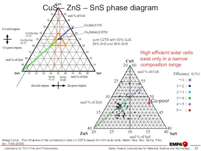
- 27. Laboratory for Thin Films and Photovoltaics Cu-poor pure CZTS with 50% CuS, 25% ZnS and 25%
- 28. Research overview Laboratory for Thin Films and Photovoltaics
- 29. Phase diagram of Cu2S – SnS2 Laboratory for Thin Films and Photovoltaics I.D. Olekseyuk, I.V. Dudchak,
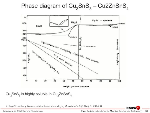
- 30. Laboratory for Thin Films and Photovoltaics K. Roy-Choudhury, Neues Jahrbuch der Mineralogie, Monatshefte 9 (1974), S.
- 31. Laboratory for Thin Films and Photovoltaics Phase diagram of kesterite – sphalerite G. Moh,Chemie der Erde
- 32. Partial density of states Laboratory for Thin Films and Photovoltaics -> orbitals that determine the band
- 34. Скачать презентацию
Outline
Motivation
Basic properties
Crystal structure and phases
Defects/Doping
Solar cells
Limiting factors
Laboratory for Thin Films
Outline
Motivation
Basic properties
Crystal structure and phases
Defects/Doping
Solar cells
Limiting factors
Laboratory for Thin Films
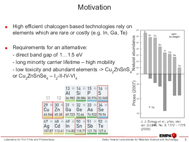
Motivation
High efficient chalcogen based technologies rely on elements which are rare
Motivation
High efficient chalcogen based technologies rely on elements which are rare
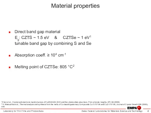
Material properties
Laboratory for Thin Films and Photovoltaics
1Chen et al., Crystal and
Material properties
Laboratory for Thin Films and Photovoltaics
1Chen et al., Crystal and
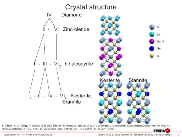
Crystal structure
Laboratory for Thin Films and Photovoltaics
S. Chen, X. G. Gong,
Crystal structure
Laboratory for Thin Films and Photovoltaics
S. Chen, X. G. Gong,
Isothermal section of the Cu2S – SnS2 - ZnS
Laboratory for Thin
Isothermal section of the Cu2S – SnS2 - ZnS
Laboratory for Thin
Isothermal section of the Cu2S – SnS2 - ZnS
Laboratory for Thin
Isothermal section of the Cu2S – SnS2 - ZnS
Laboratory for Thin
Isothermal section of the Cu2S – SnS2 - ZnS
Laboratory for Thin
Isothermal section of the Cu2S – SnS2 - ZnS
Laboratory for Thin
Isothermal section of the Cu2S – SnS2 - ZnS
Laboratory for Thin
Isothermal section of the Cu2S – SnS2 - ZnS
Laboratory for Thin
Kesterite characterization
Laboratory for Thin Films and Photovoltaics
XRD
Cu2ZnSnSe4
Cu2SnSe3
ZnSe
Kesterite characterization
Laboratory for Thin Films and Photovoltaics
XRD
Cu2ZnSnSe4
Cu2SnSe3
ZnSe
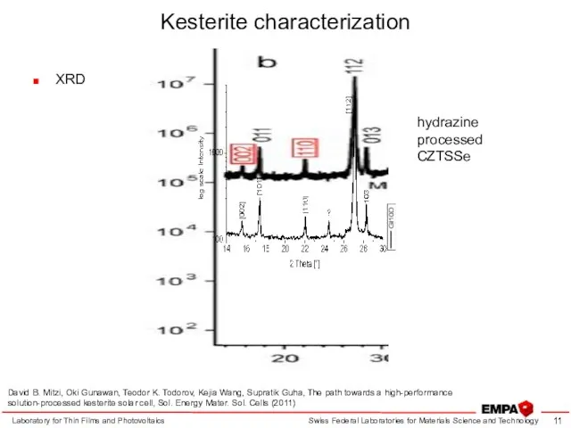
Kesterite characterization
XRD
Laboratory for Thin Films and Photovoltaics
hydrazine processed CZTSSe
David B. Mitzi,
Kesterite characterization
XRD
Laboratory for Thin Films and Photovoltaics
hydrazine processed CZTSSe
David B. Mitzi,
Kesterite characterization
Raman spectra for Cu2ZnSn(Se1-xSx)4
Laboratory for Thin Films and Photovoltaics
Stannite
x =
Kesterite characterization
Raman spectra for Cu2ZnSn(Se1-xSx)4
Laboratory for Thin Films and Photovoltaics
Stannite
x =
Kesterite characterization
Raman spectra for Cu2ZnSn(Se1-xSx)4
Laboratory for Thin Films and Photovoltaics
x =
Kesterite characterization
Raman spectra for Cu2ZnSn(Se1-xSx)4
Laboratory for Thin Films and Photovoltaics
x =
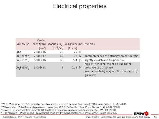
Electrical properties
Laboratory for Thin Films and Photovoltaics
1 W. K. Metzger et
Electrical properties
Laboratory for Thin Films and Photovoltaics
1 W. K. Metzger et
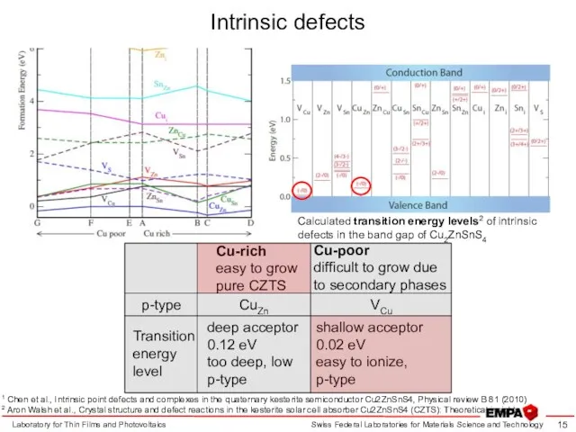
Intrinsic defects
Laboratory for Thin Films and Photovoltaics
1 Chen et al., Intrinsic
Intrinsic defects
Laboratory for Thin Films and Photovoltaics
1 Chen et al., Intrinsic
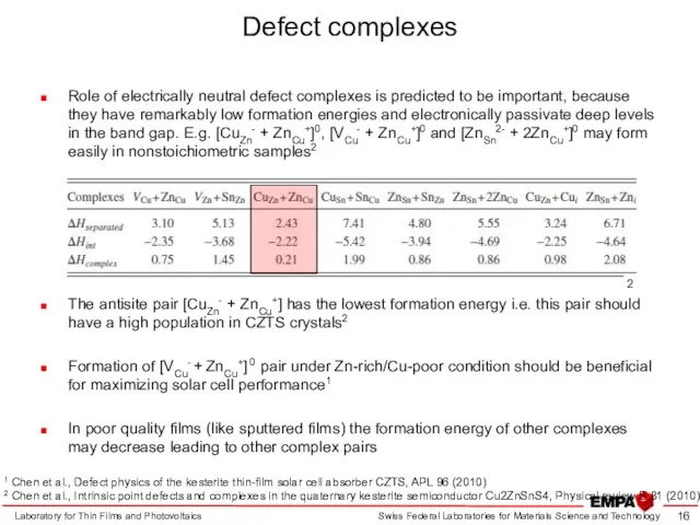
Defect complexes
Role of electrically neutral defect complexes is predicted to be
Defect complexes
Role of electrically neutral defect complexes is predicted to be
Laboratory for Thin Films and Photovoltaics
Hironori Katagiri, Kazuo Jimbo, Masami Tahara,
Laboratory for Thin Films and Photovoltaics
Hironori Katagiri, Kazuo Jimbo, Masami Tahara,
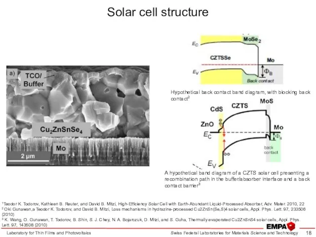
Solar cell structure
Laboratory for Thin Films and Photovoltaics
1Teodor K. Todorov, Kathleen
Solar cell structure
Laboratory for Thin Films and Photovoltaics
1Teodor K. Todorov, Kathleen
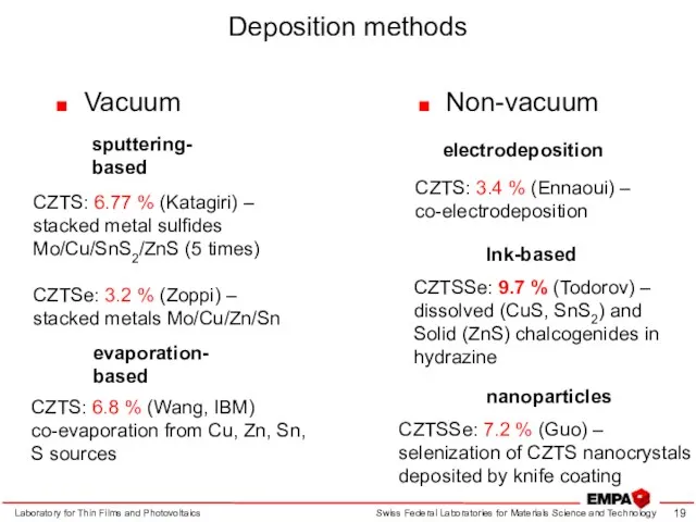
Deposition methods
Vacuum
Laboratory for Thin Films and Photovoltaics
Non-vacuum
sputtering-
based
evaporation-
based
CZTS: 6.77 % (Katagiri) –
Deposition methods
Vacuum
Laboratory for Thin Films and Photovoltaics
Non-vacuum
sputtering-
based
evaporation-
based
CZTS: 6.77 % (Katagiri) –
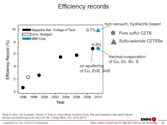
Efficiency records
Laboratory for Thin Films and Photovoltaics
David B. Mitzi, Oki Gunawan,
Efficiency records
Laboratory for Thin Films and Photovoltaics
David B. Mitzi, Oki Gunawan,
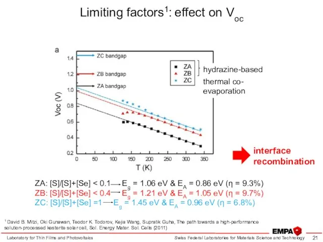
Limiting factors1: effect on Voc
Laboratory for Thin Films and Photovoltaics
1 David
Limiting factors1: effect on Voc
Laboratory for Thin Films and Photovoltaics
1 David
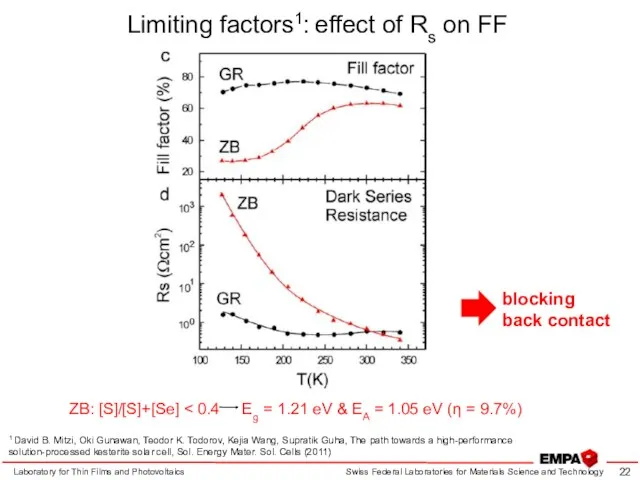
Limiting factors1: effect of Rs on FF
Laboratory for Thin Films and
Limiting factors1: effect of Rs on FF
Laboratory for Thin Films and
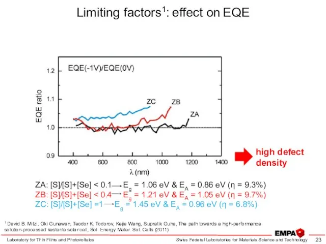
Limiting factors1: effect on EQE
Laboratory for Thin Films and Photovoltaics
1 David
Limiting factors1: effect on EQE
Laboratory for Thin Films and Photovoltaics
1 David
Conclusions
Formation and identification of parasitic phases (Cu2SnS3, Cu4SnS4, ZnS)
Metal ratio control:
Conclusions
Formation and identification of parasitic phases (Cu2SnS3, Cu4SnS4, ZnS)
Metal ratio control:
Thank you for your attention !
Laboratory for Thin Films and Photovoltaics
Thank you for your attention !
Laboratory for Thin Films and Photovoltaics
Back up sildes
Laboratory for Thin Films and Photovoltaics
Back up sildes
Laboratory for Thin Films and Photovoltaics
Laboratory for Thin Films and Photovoltaics
Cu-poor
pure CZTS with 50% CuS,
25%
Laboratory for Thin Films and Photovoltaics
Cu-poor
pure CZTS with 50% CuS,
25%
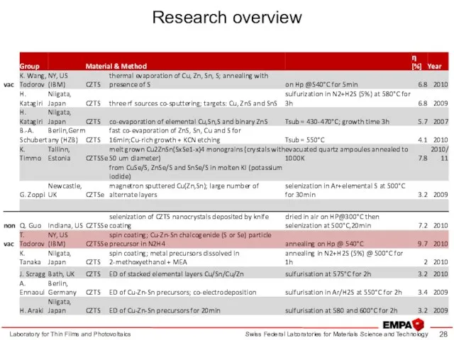
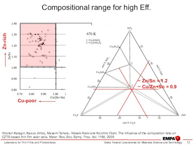
Research overview
Laboratory for Thin Films and Photovoltaics
Research overview
Laboratory for Thin Films and Photovoltaics
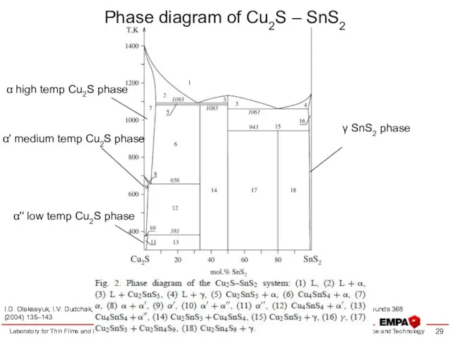
Phase diagram of Cu2S – SnS2
Laboratory for Thin Films and Photovoltaics
I.D.
Phase diagram of Cu2S – SnS2
Laboratory for Thin Films and Photovoltaics
I.D.
Laboratory for Thin Films and Photovoltaics
K. Roy-Choudhury, Neues Jahrbuch der Mineralogie,
Laboratory for Thin Films and Photovoltaics
K. Roy-Choudhury, Neues Jahrbuch der Mineralogie,
Laboratory for Thin Films and Photovoltaics
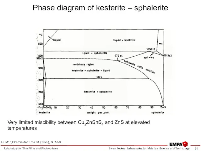
Phase diagram of kesterite – sphalerite
G.
Laboratory for Thin Films and Photovoltaics
Phase diagram of kesterite – sphalerite
G.
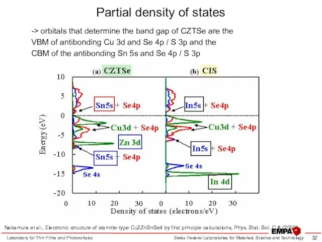
Partial density of states
Laboratory for Thin Films and Photovoltaics
-> orbitals that
Partial density of states
Laboratory for Thin Films and Photovoltaics
-> orbitals that
 Алкадиены. Непредельные углеводороды
 Классификация моторных масел
 Получение водорода. Проверка Н2 на чистоту. Практическая работа
 Симметрия в химии
 Использование потенциостата-гальваностата Elins p-20x в электрохимических исследованиях
 Переработка газа. Первичная переработка нефти. Лекция 9
 Титан және оның қорытпалары. Титаннан жасалған құралдар
 Коллигативные свойства растворов
 Окислительно-восстановительные реакции
 Распространение пламени в газах
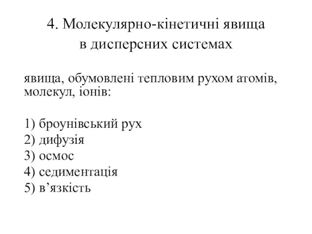 Молекулярно-кінетичні явища в дисперсних системах
 Элементы химической термодинамики. 1 и 2 законы термодинамики. Химическое равновесие
 Роль хімії у житті суспільства
 Химическая связь
 Карбоновые кислоты. (Лекция 6.3)
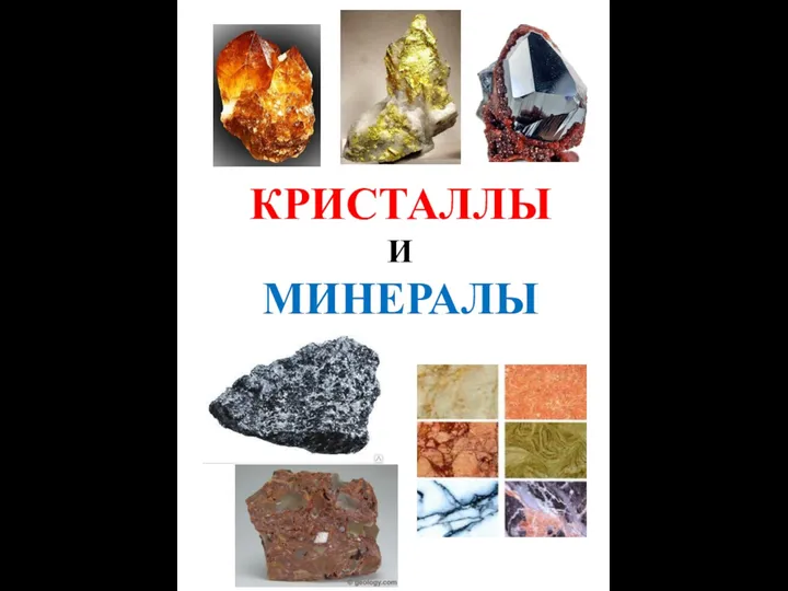 Кристаллы и минералы
 Получение полимеров из низкомолекулярных соединений
 Неон. Физические свойства
 XXI ғасыр көшбасшысы
 Электрохимические процессы. Лекция 7
 Закономерности управления каталитическими процессами
 Кислород и его применение
 Материаловедение. Контрольная работа
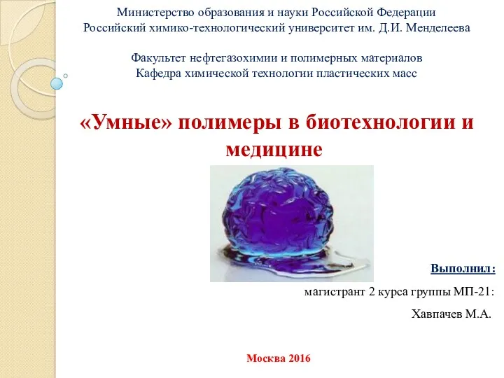 Умные полимеры в биотехнологии и медицине
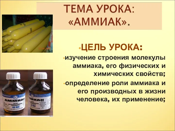 Аммиак. 9 класс
 Гидролиз органических и неорганических соединений
 Оксиды
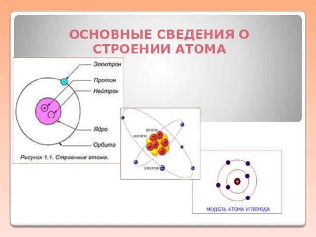 Основные сведения о строении атома