Cross-section sample preparation using focused ion beam system (FIB) for transmission electron microscopy (TEM) презентация
- Cross-section sample preparation using focused ion beam system (FIB) for transmission electron microscopy (TEM)

Содержание
- 2. What is TEM? TEM Hitachi HT 7700 What can be observed by TEM: Thin films and
- 3. Supporting grid for TEM specimens TEM specimen holder
- 4. Examples Ni nanoparticles (catalysts) and carbon nanotubes Ni-Ti thin foil Neonothopanus nambi (lat.) biological specimen Co-Al2O3
- 5. What is “cross-section”? cross-section is basic method of observation multi layers structures cross-section method allows to
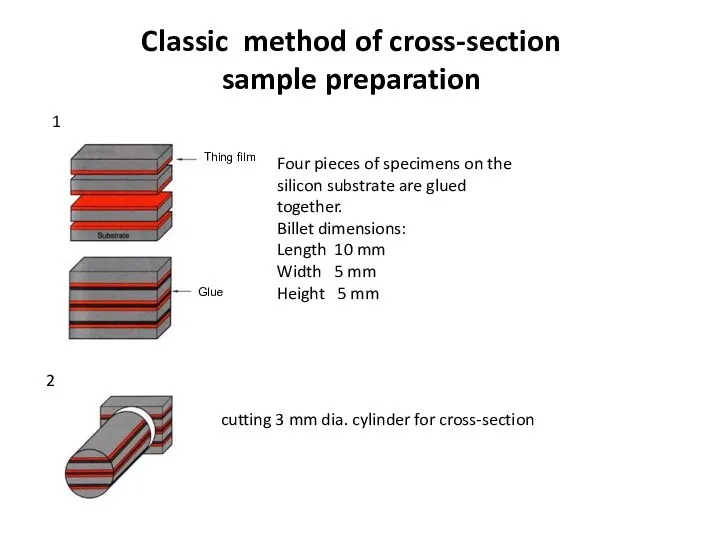
- 6. Classic method of cross-section sample preparation Four pieces of specimens on the silicon substrate are glued
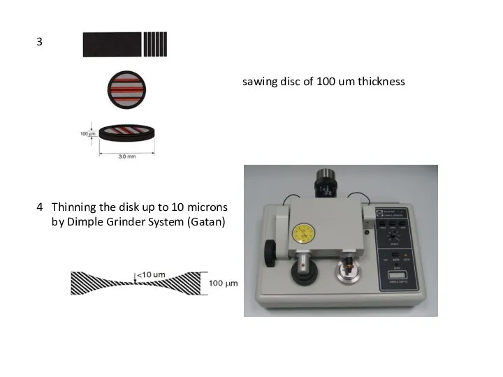
- 7. 3 sawing disc of 100 um thickness 4 Thinning the disk up to 10 microns by
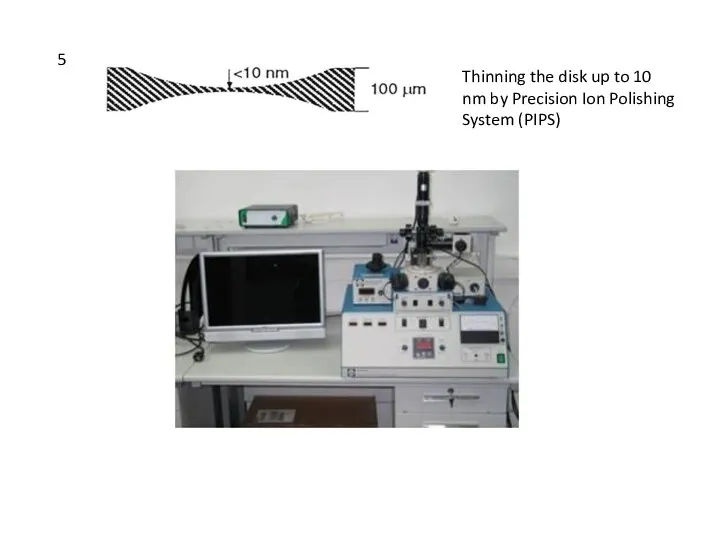
- 8. 5 Thinning the disk up to 10 nm by Precision Ion Polishing System (PIPS)
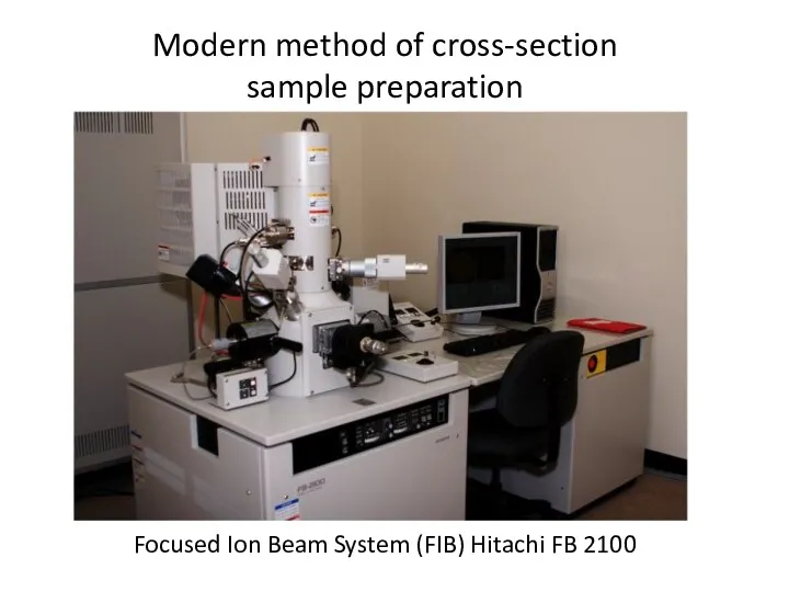
- 9. Modern method of cross-section sample preparation Focused Ion Beam System (FIB) Hitachi FB 2100
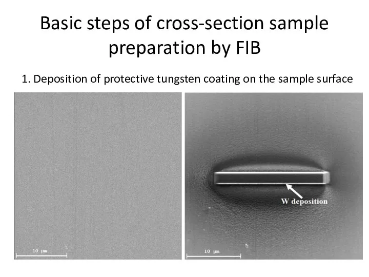
- 10. Basic steps of cross-section sample preparation by FIB 1. Deposition of protective tungsten coating on the
- 11. 2. Cutting half-finished (lamella)
- 12. 2. Cutting lamella (continuation)
- 13. 3. Fixing microprobe
- 14. 4. Cutting left side and removing lamella
- 15. 5. Fixing lamella on the toothed semicircle
- 16. 6. Cutting and removing microprobe
- 17. 7. Thinning specimen to 50-100 nm
- 18. Finish result Область просмотра в ПЭМ Disadvantages of FIB method Damaging top layer during deposition tungsten
- 19. Some features sample preparation with thin layers (thickness less than 300 nm)
- 22. Pre-sputtering of Ge protective layer
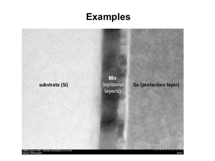
- 23. substrate (Si) Ge (protection layer) Mn (epitaxial layers) Examples
- 24. substrate (Si) Ge (protection layer) Co Pt
- 25. comparison of the two methods Classic method FIB method
- 27. Скачать презентацию
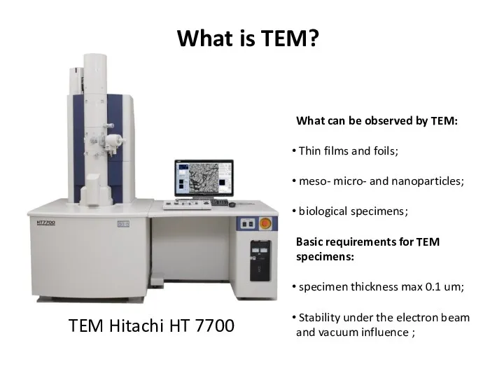
What is TEM?
TEM Hitachi HT 7700
What can be observed by TEM:
What is TEM?
TEM Hitachi HT 7700
What can be observed by TEM:
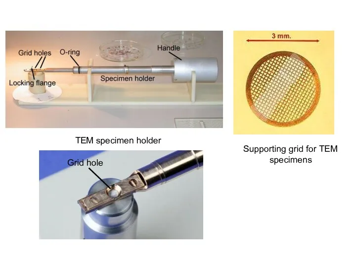
Supporting grid for TEM specimens
TEM specimen holder
Supporting grid for TEM specimens
TEM specimen holder
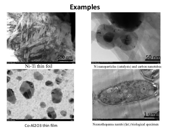
Examples
Ni nanoparticles (catalysts) and carbon nanotubes
Ni-Ti thin foil
Neonothopanus nambi (lat.) biological
Examples
Ni nanoparticles (catalysts) and carbon nanotubes
Ni-Ti thin foil
Neonothopanus nambi (lat.) biological
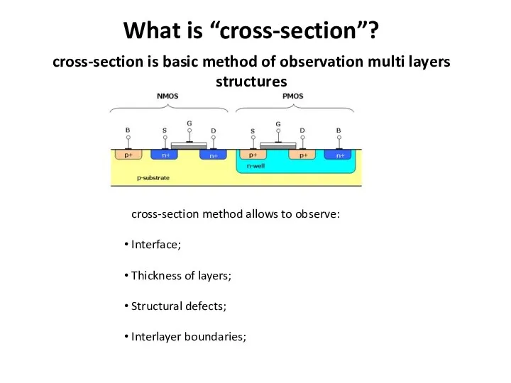
What is “cross-section”?
cross-section is basic method of observation multi layers structures
What is “cross-section”?
cross-section is basic method of observation multi layers structures
Classic method of cross-section sample preparation
Four pieces of specimens on
Classic method of cross-section sample preparation
Four pieces of specimens on
3
sawing disc of 100 um thickness
4
Thinning the disk up to 10
3
sawing disc of 100 um thickness
4
Thinning the disk up to 10
5
Thinning the disk up to 10 nm by Precision Ion Polishing
5
Thinning the disk up to 10 nm by Precision Ion Polishing
Modern method of cross-section sample preparation
Focused Ion Beam System (FIB)
Modern method of cross-section sample preparation
Focused Ion Beam System (FIB)
Basic steps of cross-section sample preparation by FIB
1. Deposition of protective
Basic steps of cross-section sample preparation by FIB
1. Deposition of protective
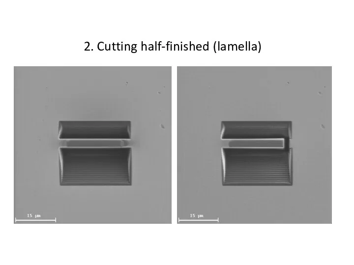
2. Cutting half-finished (lamella)
2. Cutting half-finished (lamella)
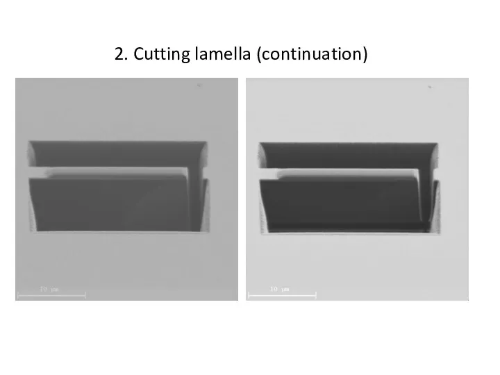
2. Cutting lamella (continuation)
2. Cutting lamella (continuation)
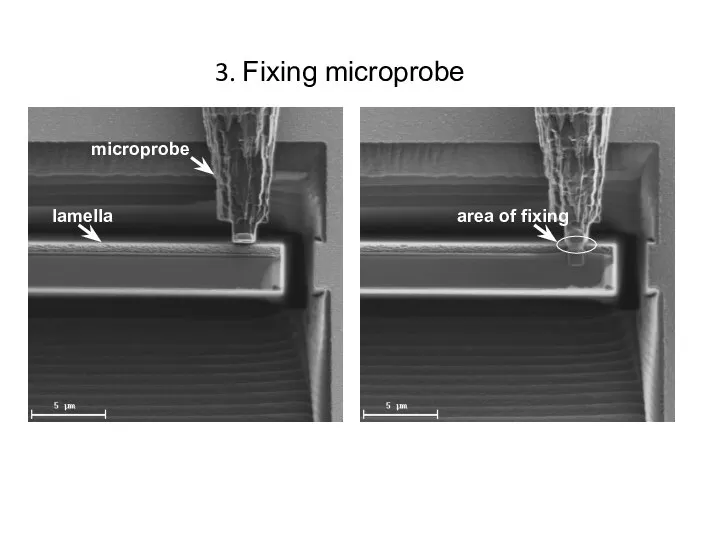
3. Fixing microprobe
3. Fixing microprobe
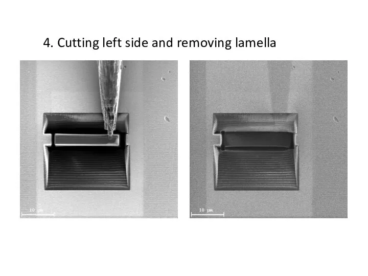
4. Cutting left side and removing lamella
4. Cutting left side and removing lamella
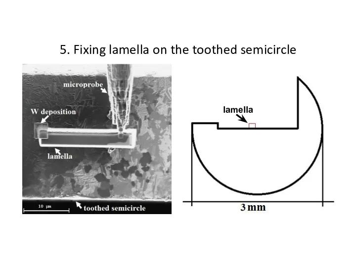
5. Fixing lamella on the toothed semicircle
5. Fixing lamella on the toothed semicircle
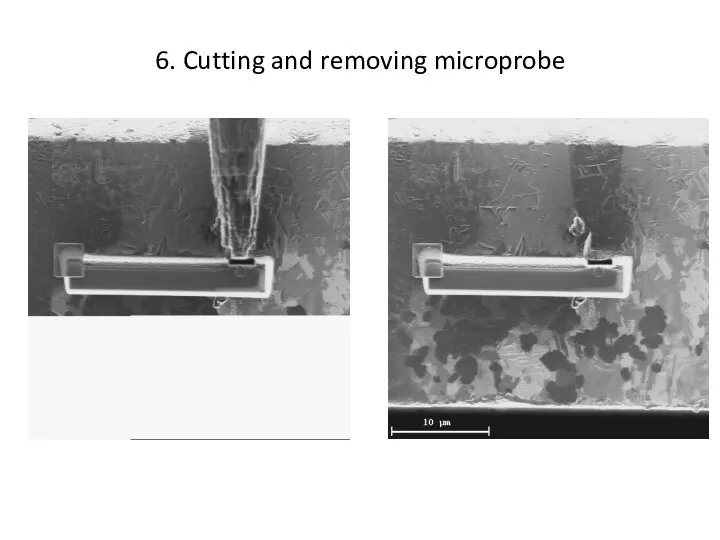
6. Cutting and removing microprobe
6. Cutting and removing microprobe
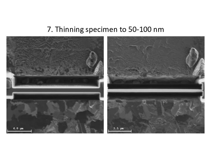
7. Thinning specimen to 50-100 nm
7. Thinning specimen to 50-100 nm
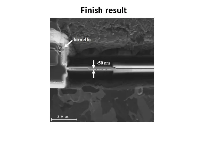
Finish result
Область просмотра в ПЭМ
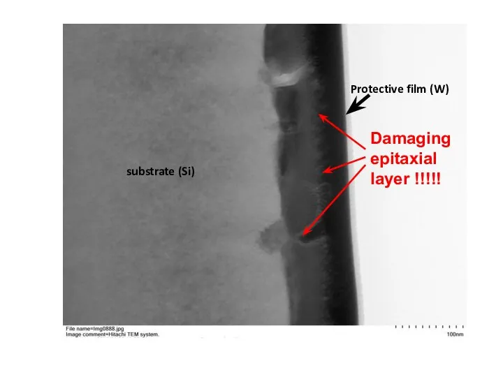
Disadvantages of FIB method
Damaging top layer during
Finish result
Область просмотра в ПЭМ
Disadvantages of FIB method
Damaging top layer during
Some features sample preparation with thin layers (thickness less than 300
Some features sample preparation with thin layers (thickness less than 300
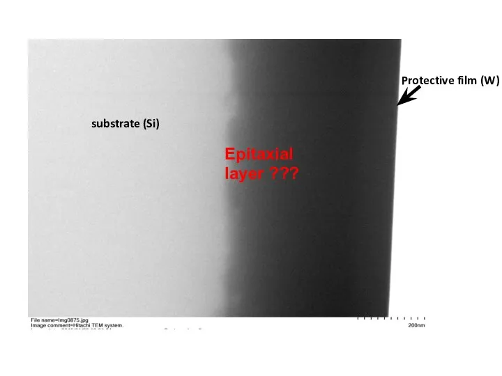
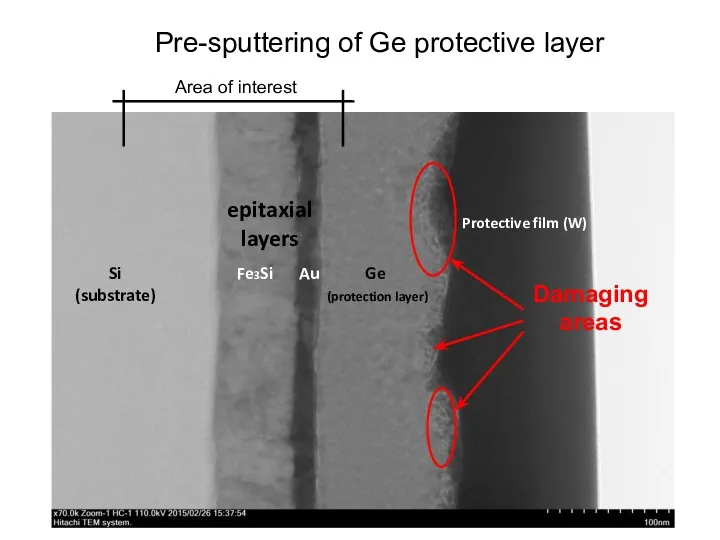
Pre-sputtering of Ge protective layer
Pre-sputtering of Ge protective layer
substrate (Si)
Ge (protection layer)
Mn
(epitaxial layers)
Examples
substrate (Si)
Ge (protection layer)
Mn
(epitaxial layers)
Examples
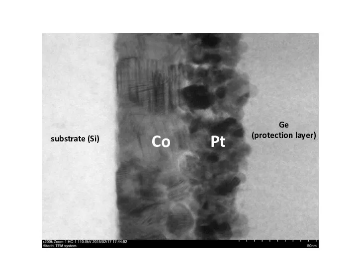
substrate (Si)
Ge
(protection layer)
Co
Pt
substrate (Si)
Ge
(protection layer)
Co
Pt
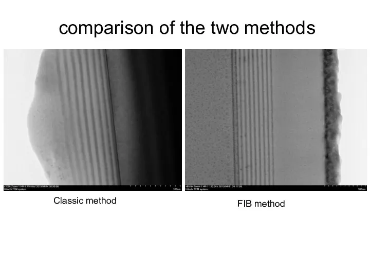
comparison of the two methods
Classic method
FIB method
comparison of the two methods
Classic method
FIB method
 Непредельные углеводороды этиленового ряда (олефины, алкены)
 Класифікація неорганічних сполук. Оксиди
 Изучение физико-химических свойств мицеллярных растворов индивидуальных ПАВ, композиций различных ПАВ
 Строение атомов. Понятие о квантовой механике
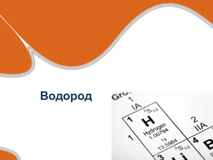 Водород. Распространенность в природе
 Решение задач по теме: «Электролиз»
 Элементы триады железа: Fe, Co, Ni. (Лекция 16)
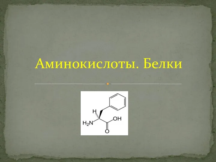 Аминокислоты. Белки
 Properties of Atoms and the Periodic Table
 Синтетические волокна
 Методы составления уравнений окислительно-восстановительных реакций. Лекция №20
 Химия. Дисперсные системы. Растворы
 Углеводы. Общая формула углеводов Сn(H2O)m
 Петрология. Классификации магматических горных пород
 Неметаллы: общая характеристика. 9 класс
 Непредельные углеводороды. Этилен. 9 класс
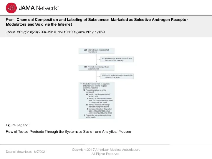 Figure
 Лекция 7. Электрофильное замещение в ароматических системах
 Кристаллическое строение и свойства металлов
 Классификация химических реакций в органической химии
 α-Аминокислоты. Белки
 Реакции ионного обмена. Теория химического строения органических соединений. 9 класс
 Газовые гидраты
 Виведення молекулярної формули речовини за загальною формулою гомологічного ряду та густиною або відносною густиною
 Склад і основні фізико-хімічні властивості молочного білку
 Методы определения механических свойств полимерных композиционных материалов
 Решение задач на определение массовой и объемной доли вещества для смесей и растворов
 Основные классы неорганических соединений